
The same package does not guarantee the same startup behavior. RK806S-5 has fixed sequencing for RK3576 and cannot simply be replaced by RK806-2. Confirm the exact part, OTP configuration and reference circuit before reviewing external components.
Based on the Chinese and English RK3576 Hardware Design Guide V1.1 (2024-05-28), for SoC-board design. CM5 carriers must follow the module interface; Sige5 can establish a software/peripheral baseline. This guide does not prescribe one SDK/BSP or kernel for every product; verify each board. Values are source references, not ArmSoM measurements.
RK3576_Hardware_Design_Guide_V1.1_20240528_EN.pdf · §2.2.3–2.2.4
Communication and input rails
The reference uses I2C with CS connected to VCCA at startup. VCCA (Pin21) must be the highest supply, or above Vmax−0.3V, and rise before or with the other inputs. PLDO6 supplies communication IO and must match the AP domain. The PMIC input range of 2.7–5.5V does not replace startup conditions: the VDC description also requires VCCA/VCC1/VCC2 above 3.0V.
Power control and reset belong together
VDC threshold is 0.8V; the design recommendation is above 1V and no higher than VCCA. Holding it high may prevent normal shutdown; validate the source RC auto-start circuit. PWRON has about 45kΩ internal pull-up, defaults to 20ms low for startup and 6s for forced shutdown, configurable to 6/8/10/12s. After EXT_EN rises, VCCA/VCC1/VCC2 must exceed 3V within 100ms. Keep RESETB total capacitance ≤0.3μF.
Feedback and an unresolved source discrepancy
FB versus VOUT selection depends on the specific BUCK and OTP; do not reconnect all channels uniformly. The external-divider example is Vout=(R1/R2+1)×0.5V, with resistors from 10kΩ to 1MΩ. Figure 2-49 shows 0.22μH for BUCK1–4 while the prose says 0.24μH. Both are retained here; resolve selection using the current reference BOM, PMIC specification and vendor confirmation. COT feedback requires joint layout and ripple review.
Design parameters and review table
| Item | Value or net | Review note |
|---|---|---|
| Input/package | 2.7–5.5V; QFN68 7×7mm | Chip specification, not board input |
| BUCK ratings | 1:6.5A; 2–4:5A; 5–10:3A | Maximum rating is not sustained design load |
| Default interface | I2C / CS→VCCA | Match OTP, AP levels and startup configuration |
Reference circuits and figures
The reference pages below contain the relevant circuit or timing figures; click for full resolution. Designators and component values belong to the reference design, not an ArmSoM product schematic.
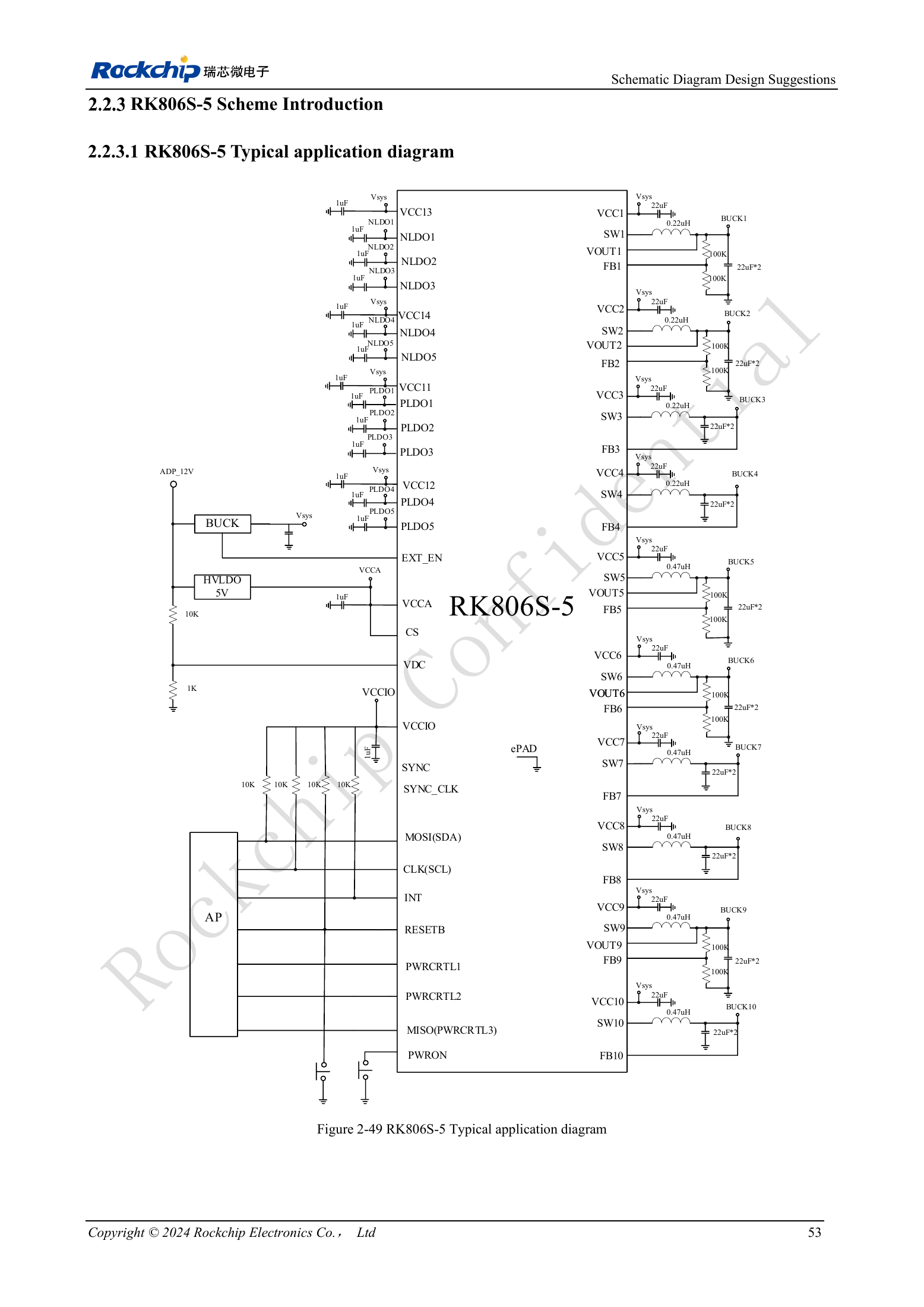
English original · PDF 72 · 2-49
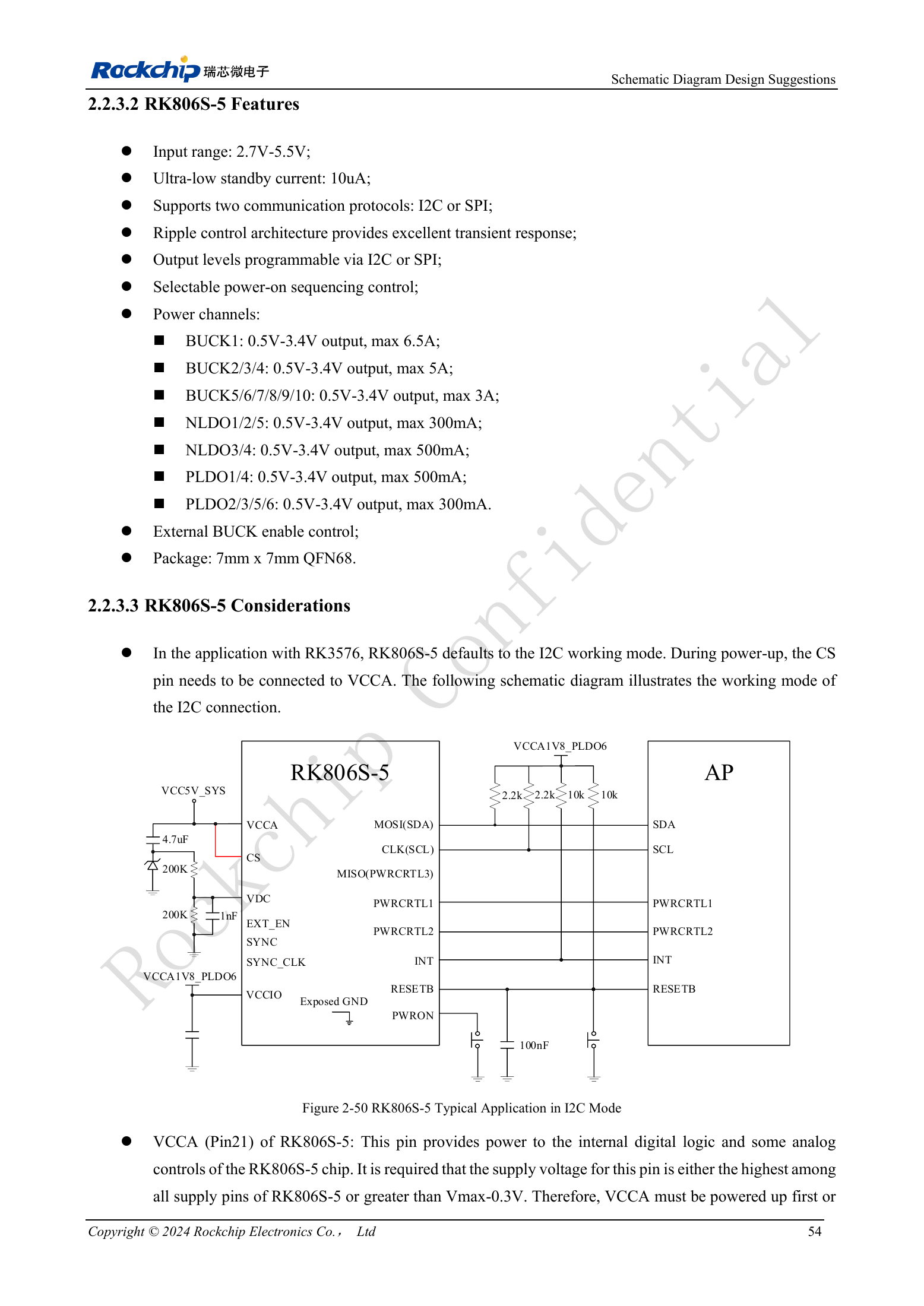
English original · PDF 73 · 2-50
ArmSoM products and development path
CM5 brings integrated computing to a custom carrier; Sige5 supports initial Linux and peripheral evaluation. SoC interface capability does not mean both products expose it. Check connectors, board revision and system image before purchasing or layout.
Series reading order
- RK3576 hardware design series: from minimum system to DDR and USB
- RK3576 minimum system: from schematic review to repeatable first boot
- RK3576 clock design: 24MHz crystal, 32kHz standby and peripheral clocks
- RK3576 reset design: NPOR, RK806S-5, watchdog and thermal shutdown
- RK3576 boot and debug design: straps, Maskrom, UART and JTAG
- RK3576 rails and decoupling: CPU, GPU, NPU and LOGIC supply planning
- RK3576 power sequencing and standby: reset, retained rails and wake paths
- RK3576 DDR circuits and power: LPDDR4, LPDDR4X and LPDDR5
- RK3576 DDR PCB routing: impedance, length, return paths and PDN
- RK3576 USB and Type-C hardware supplement: multiplexing, recovery and protection