
“Lower voltage first” cannot replace individual PHY requirements. Map each rail dependency, then review cold start, shutdown and every standby/wake configuration separately.
Based on the Chinese and English RK3576 Hardware Design Guide V1.1 (2024-05-28), for SoC-board design. CM5 carriers must follow the module interface; Sige5 can establish a software/peripheral baseline. This guide does not prescribe one SDK/BSP or kernel for every product; verify each board. Values are source references, not ArmSoM measurements.
RK3576_Hardware_Design_Guide_V1.1_20240528_EN.pdf · §2.2.1; §2.2.4
Sequence exceptions and reset release
DDRPHY follows DVDD→CKE_VDDQ→VDDQ/CK_VDDQ; USB2 follows 0.75→1.8→3.3V, UFS and USB3/DP 0.85→1.8V. MIPIDCPHY has a special low-voltage→1.8→1.2V sequence, not numerical ascending order. Release RESET_L at least 1ms after the last rail stabilizes. The guide suggests a practical 5–200ms delay, subject to external device requirements.
Retained rails depend on the wake source
Minimum standby retains DDRPHY_CKE_VDDQ, PMU_LOGIC_DVDD0V75, PMUIO0_VCC1V8 and PMUIO1_VCC, primarily using PMUIO interrupt wake. USB HID wake also requires oscillator and USB2 PHY supplies. Interrupts through VCCIO0–7 need the corresponding IO, LOGIC and LOGIC_MEM. The minimum rail list cannot be applied to every product.
GPIO retention and shutdown tests
The Wi-Fi example first drives WIFI_REG_ON_H/BT_REG_ON_H high and enables GPIO retention before removing relevant main logic/oscillator supplies, while retaining peripheral power and IO. It does not prove an arbitrary BSP implements this. Assert RESET_L before shutdown. Keep the GPIO3.3V–PMUIO0_1.8V and USB3.3V–USB1.8V differences within the guide’s 2V limits. Check back-powering from peripherals that remain powered.
Design parameters and review table
| Item | Value or net | Review note |
|---|---|---|
| Final rail to reset | ≥1ms | Practical reference 5–200ms |
| First shutdown step | RESET_L = LOW | Then remove rails per domain rules |
| PMIC sequence | RK806S-5 | Fixed configuration; not RK806-2 |
Reference circuits and figures
The reference pages below contain the relevant circuit or timing figures; click for full resolution. Designators and component values belong to the reference design, not an ArmSoM product schematic.
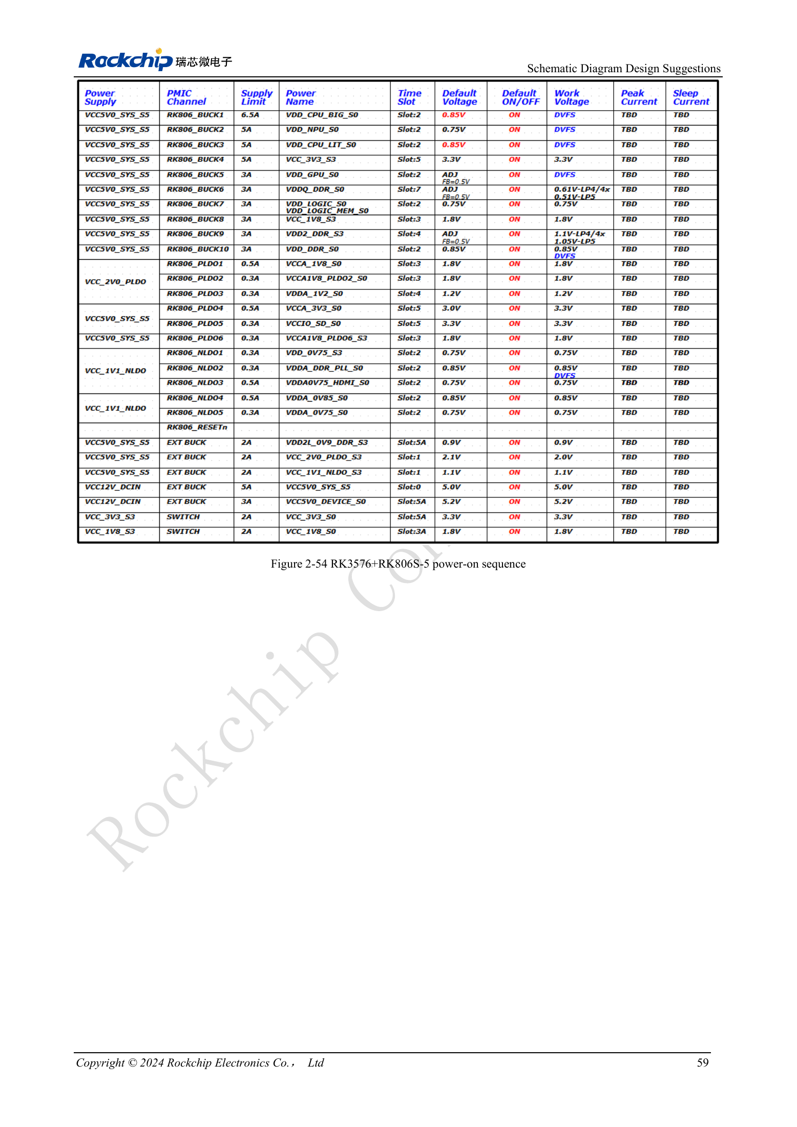
English original · PDF 78 · 2-54
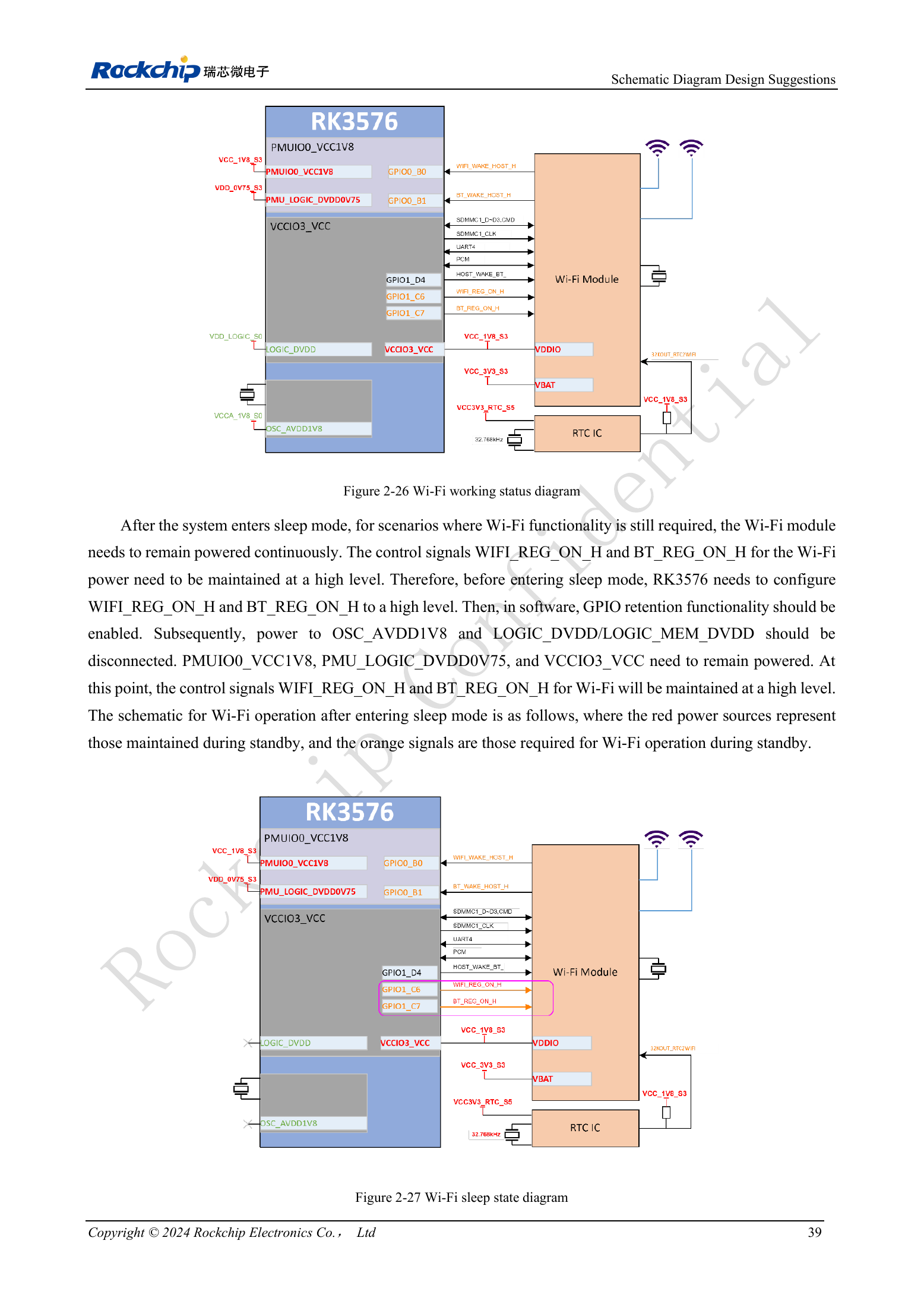
English original · PDF 58 · 2-26 / 2-27
ArmSoM products and development path
CM5 brings integrated computing to a custom carrier; Sige5 supports initial Linux and peripheral evaluation. SoC interface capability does not mean both products expose it. Check connectors, board revision and system image before purchasing or layout.
Series reading order
- RK3576 hardware design series: from minimum system to DDR and USB
- RK3576 minimum system: from schematic review to repeatable first boot
- RK3576 clock design: 24MHz crystal, 32kHz standby and peripheral clocks
- RK3576 reset design: NPOR, RK806S-5, watchdog and thermal shutdown
- RK3576 boot and debug design: straps, Maskrom, UART and JTAG
- RK3576 rails and decoupling: CPU, GPU, NPU and LOGIC supply planning
- RK3576 and RK806S-5: PMIC selection, control pins and feedback
- RK3576 DDR circuits and power: LPDDR4, LPDDR4X and LPDDR5
- RK3576 DDR PCB routing: impedance, length, return paths and PDN
- RK3576 USB and Type-C hardware supplement: multiplexing, recovery and protection