
Clock faults can cause boot, USB or wake-up failures. Review oscillator circuitry, accuracy, output voltage and the sources that remain active in standby; the presence of a 24MHz crystal alone is insufficient.
Based on the Chinese and English RK3576 Hardware Design Guide V1.1 (2024-05-28), for SoC-board design. CM5 carriers must follow the module interface; Sige5 can establish a software/peripheral baseline. This guide does not prescribe one SDK/BSP or kernel for every product; verify each board. Values are source references, not ArmSoM measurements.
RK3576_Hardware_Design_Guide_V1.1_20240528_EN.pdf · §2.1.1
Critical parts around the passive crystal
The 22Ω resistor in series with XOUT_24M limits overdrive; do not arbitrarily change the 510kΩ resistor between XOUT and XIN. Crystal load capacitance CL must not exceed 12pF. Select and verify CL1/CL2 for the actual crystal; 18pF is a reference-design value. Use C0G/NP0 capacitors and a four-pad crystal with both ground pads properly connected. Probe capacitance can disturb oscillation.
Active input and duty cycle
The reference active-clock voltage is 1.35–1.8V, with 50% duty cycle and 20ppm accuracy. The guide observes bypassed 24MHz at REF_CLK0_OUT (Pin V29) while adjusting R1100; this is not a universal register command. A 0.8V input may not reach 50% duty cycle, so oscillation alone does not demonstrate compliance.
Review standby and output clocks together
Before stopping 24MHz, switch to PMU_PVTM or external 32.768kHz and verify that wake sources do not require 24MHz. Minimum standby relies on PMUIO0/1 interrupts. Disable the GPIO internal pull-down for an open-drain RTC connected to CLK32K_IN. CLK0/1_32K_OUT is not guaranteed after 24MHz stops. Check pin multiplexing and peripheral voltage for camera and Ethernet clock outputs as well.
Design parameters and review table
| Item | Value or net | Review note |
|---|---|---|
| Crystal tolerance | ≤20ppm | At room temperature, per source |
| External standby clock | 32.768kHz ±30ppm; 45–55% | Amplitude 0.7×VDD to VDD; VDD=PMUIO0 |
| Reference outputs | REF_CLK0/1/2_OUT | 12/24/25/26/27/37.125/74.25/10/20/40/50/58.5/100MHz |
| Camera clocks | CAM_CLK0/1/2_OUT | Default 24MHz; alternatives 27/37.125/74.25MHz |
Reference circuits and figures
The reference pages below contain the relevant circuit or timing figures; click for full resolution. Designators and component values belong to the reference design, not an ArmSoM product schematic.
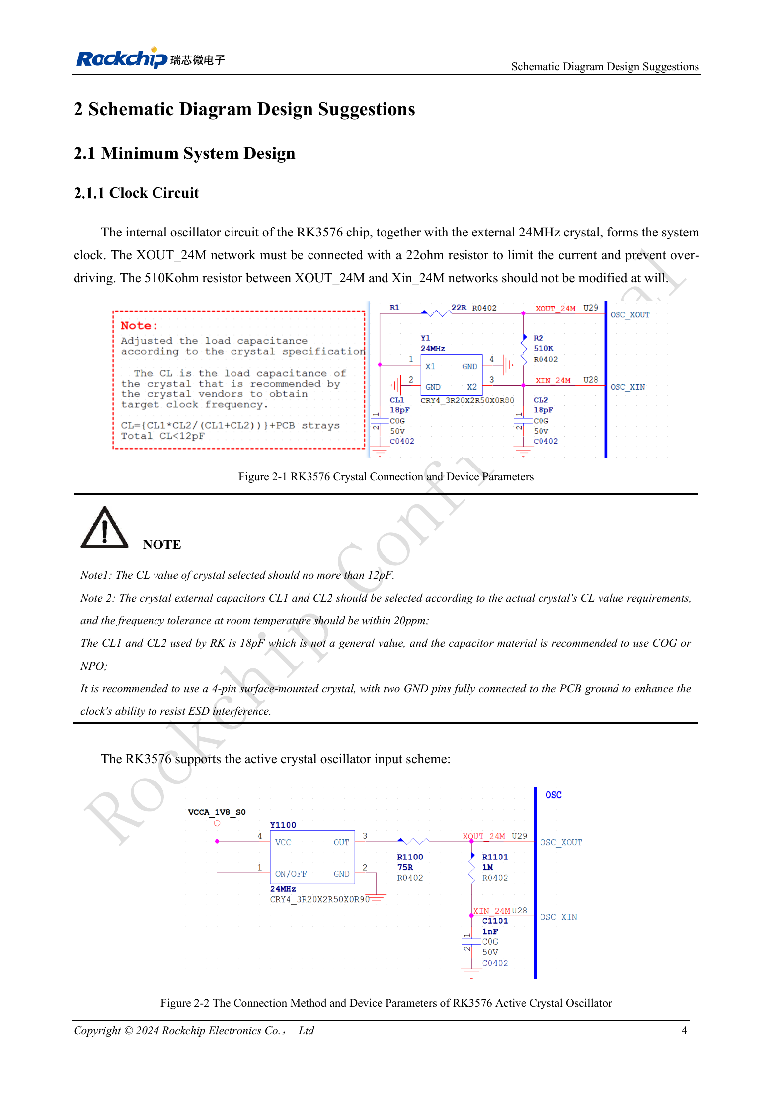
English original · PDF 23 · 2-1 / 2-2
ArmSoM products and development path
CM5 brings integrated computing to a custom carrier; Sige5 supports initial Linux and peripheral evaluation. SoC interface capability does not mean both products expose it. Check connectors, board revision and system image before purchasing or layout.
Series reading order
- RK3576 hardware design series: from minimum system to DDR and USB
- RK3576 minimum system: from schematic review to repeatable first boot
- RK3576 reset design: NPOR, RK806S-5, watchdog and thermal shutdown
- RK3576 boot and debug design: straps, Maskrom, UART and JTAG
- RK3576 rails and decoupling: CPU, GPU, NPU and LOGIC supply planning
- RK3576 and RK806S-5: PMIC selection, control pins and feedback
- RK3576 power sequencing and standby: reset, retained rails and wake paths
- RK3576 DDR circuits and power: LPDDR4, LPDDR4X and LPDDR5
- RK3576 DDR PCB routing: impedance, length, return paths and PDN
- RK3576 USB and Type-C hardware supplement: multiplexing, recovery and protection