
Based on the Chinese RK3588S Hardware Design Guide V1.2 (2023-12-14) for circuit and PCB review. CM7S carriers must follow module interface definitions; Sige7S supports software and peripheral evaluation. SoC capabilities are not a board connector list. Verify SDK/BSP, kernel, board revision, firmware and multiplexing. Values are source references, not ArmSoM hardware measurements.
RK3588S Hardware Design Guide V1.2 (2023-12-14), CN · §3.1–3.2
Both references use second-order HDI
The RK3588S guide presents 10-layer and 8-layer second-order HDI, not the RK3588 8-layer through-hole example. Reference thickness is 1.6mm; keep signals adjacent to ground and the stack symmetric. Page 147 incorrectly calls the bottom of the eight-layer stack L9. Check the diagram and fabricator stack instead of copying that label.
Separate BGA escape from carrier routing
The outer two ball rows can escape on the top layer; minimize transitions for fast interfaces. Actual width, microvias, buried vias and antipads depend on fabrication and impedance calculations. A CM7S carrier routes from module connectors rather than duplicating RK3588S BGA escape. Review the combined module, connector and carrier channel.
Design parameters and review table
| Item | Source reference |
|---|---|
| Reference stackups | 10-layer / 8-layer second-order HDI |
| Example board thickness | 1.6mm |
| Routing length scope | PCB + vias + package |
Source figures
No corresponding English design guide was found for this batch. All four editions use Chinese source screenshots with localized captions. Open an image for full resolution; the article text and parameter tables remain copyable. Page references are physical PDF pages.
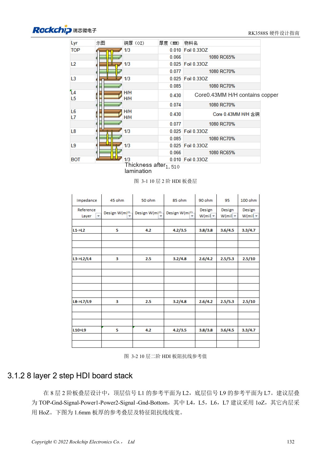
Chinese original · PDF 147 · 3-1
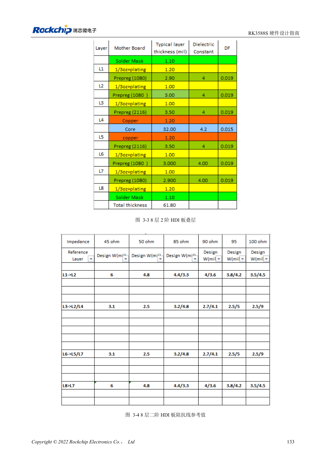
Chinese original · PDF 148 · 3-3
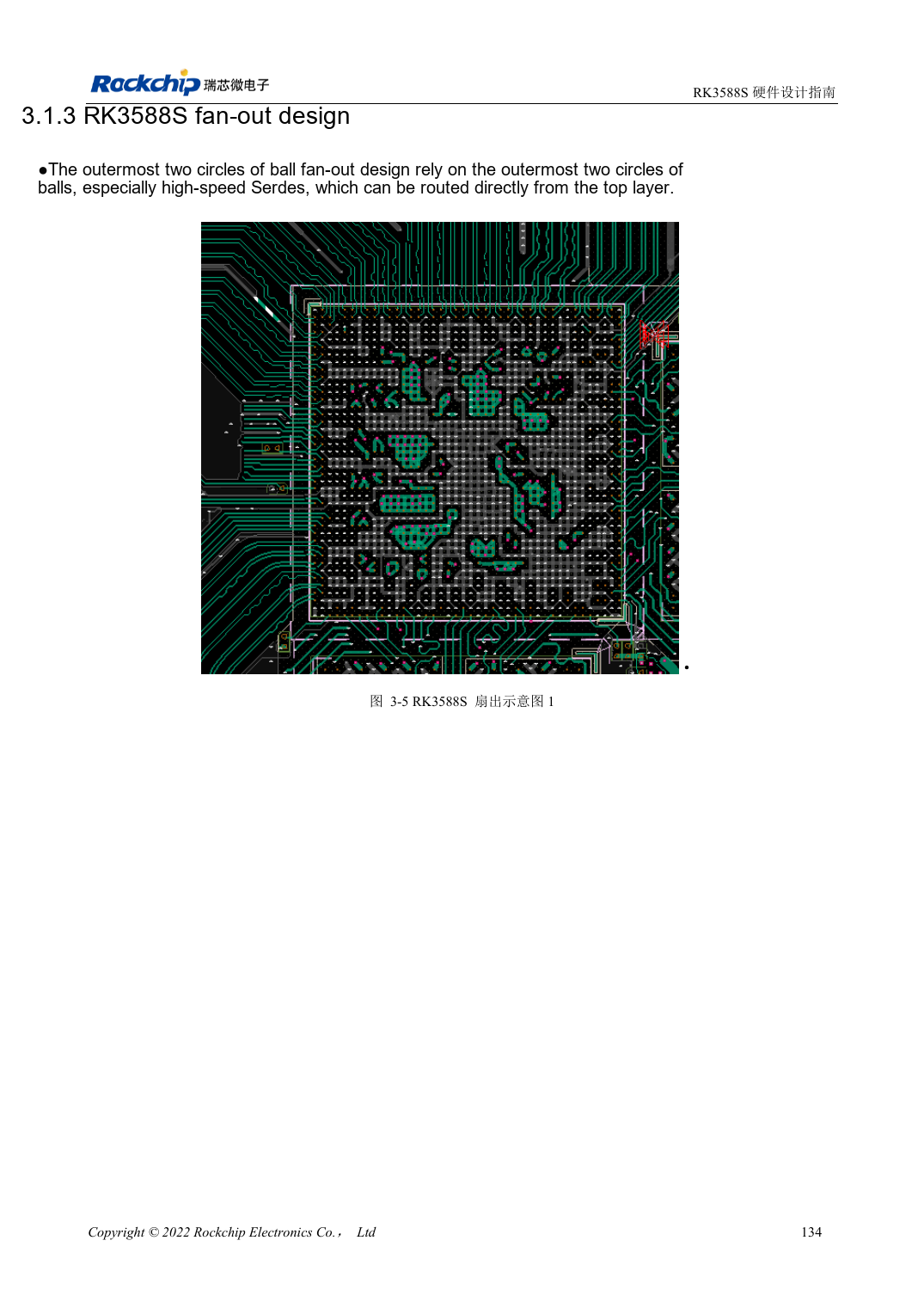
Chinese original · PDF 149 · 3-5
ArmSoM development path
CM7S supports custom carriers: first identify supplies, DDR and boot circuits already integrated in the module, then design outside its connectors. Sige7S provides a starting point for software and peripheral evaluation. For both products, verify exposed interfaces, pin assignments, levels, system images and cooling against the relevant revision. A chip reference schematic is not a product wiring diagram.