
Scope and sources
This is a task-focused engineering guide, not a page-by-page translation of the complete PDF. Source examples are not ArmSoM measurements. Check voltages, pins, SDK/BSP and kernel against the actual board revision.
Rockchip: RK3576_Hardware_Design_Guide_V1.1_20240528_CN.pdf · V1.1 · §2.1, §2–3
Define the real endpoint
The source covers interface circuits in §2.3, signals at 8GT/s and above in §3.4, and module-specific PCB guidance in §3.5. Begin with the peripheral, operating mode, connector and cable. Resources shown in a chip diagram are not necessarily all exposed or simultaneously available on a module.
List PHY sharing, control buses, supplies and software dependencies for cameras, displays, storage and networking. Check CM5 module pins or the actual Sige5 board revision before allocating resources.
Review the schematic and layout together
| Area | Schematic review | Layout review |
|---|---|---|
| Differential channel | Direction, coupling and protection | Impedance, reference planes, vias and pad discontinuities |
| Peripheral control | Reset, enable, buses and voltage domains | Separation and accessible test points |
| Connector | Exact part, pins and shield connection | Footprint, return path and orientation |
| Power | Peak current and sequencing | Decoupling, current loops and heat path |
The guide discusses BGA pads, glass-weave effects, differential vias, coupling capacitors, ESD parts and connector pads. Local reference-plane voiding addresses specific parasitics; it is not permission to split ground under arbitrary high-speed routes.
Budget the complete channel
Include module traces, connectors, carrier, cable and peripheral PCB. Length matching is only one constraint: stubs, reference changes and protection capacitance can also reduce margin. Obtain numerical limits from the relevant interface mode and the fabricator’s stackup calculation, not from an unrelated bus.
Close the validation loop
Test each interface at the intended rate, then test adjacent interfaces and application concurrency. Failures under combined load also require investigation of power transients, heat, bandwidth and drivers. Record cables, peripherals, BSP and board revisions. Reducing speed may help diagnosis, but does not pass the original speed requirement. Revalidate the actual channel when moving a CM5 or Sige5 prototype into a custom product.
Source illustration
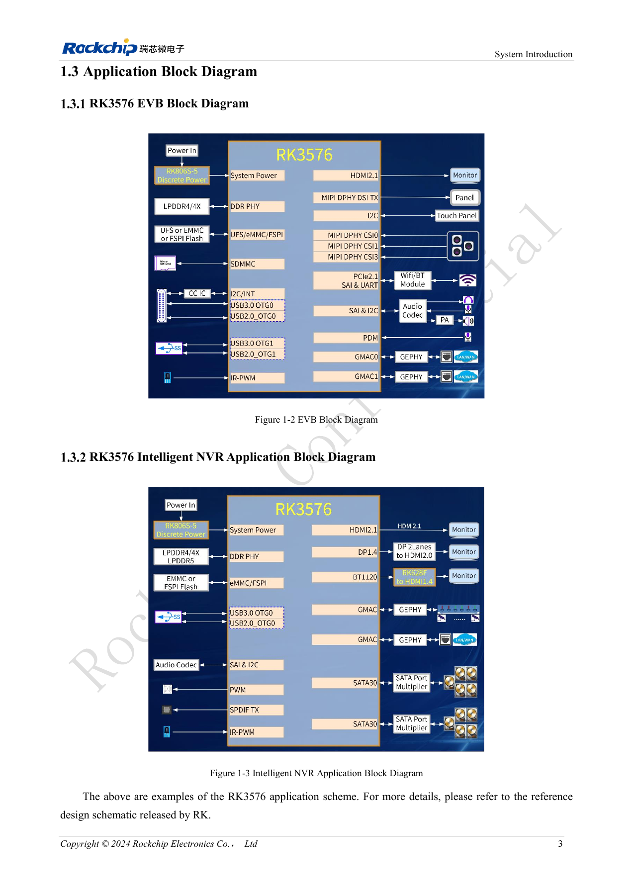
Original from the English document, shared by EN/RU/DE. Reference design, not an ArmSoM board schematic.
RK3576_Hardware_Design_Guide_V1.1_20240528_EN.pdf · PDF p. 22.
Products and development resources
- CM5 — Product page · Documentation
- Sige5 — Product page · Documentation
Continue this series
- RK3576 hardware bring-up: minimum system and first-power checks
- ArmSoM CM5 carrier-board checklist: power, boot and interface planning
- RK3588S hardware design: from a reference circuit to a CM7s carrier
- RK3588 edge-AI hardware: plan power, cooling and expansion together
- RK3588 high-speed PCB review: stackup, impedance and routing
- RK3506 industrial HMI hardware: choosing a CM1 or Forge1 development path
- RK3308 hardware variants: compatibility checks for P2 Pro audio projects
- RK3588S versus RK3588S2: what to check before a hardware revision
- Rockchip prototype to production: process requirements and test records
RK3576 high-speed interfaces: impedance, return paths, stubs and channel review
Based on the Chinese and English RK3576 Hardware Design Guide V1.1 (2024-05-28), for SoC-board design. CM5 carriers must follow the module interface; Sige5 can establish a software/peripheral baseline. This guide does not prescribe one SDK/BSP or kernel for every product; verify each board. Values are source references, not ArmSoM measurements.
RK3576_Hardware_Design_Guide_V1.1_20240528_EN.pdf · §3.3–3.4
Differential pairs do not all share one rule
Reference values include PCIe data 85Ω, PCIe REFCLK 100Ω, eDP 90Ω and dedicated DP 100Ω or USB-shared DP 95Ω. Define constraints by net class rather than setting every pair to 100Ω. Length includes vias and packages. Intra-pair matching and matching between pairs are distinct constraints. W means trace width and spacing means airgap, not centre distance.
Return continuity matters more than neat meanders
Do not cross reference-plane gaps; generic guidance keeps fast signals at least 40mil from a plane edge. Add nearby ground vias at layer changes. Test points, connectors and component pads create stubs or discontinuities. Local relief under large pads requires reference geometry and simulation, not removal of ground beneath the entire pair. The guide calls for SI assessment of via stubs over 12mil.
Connect schematic and layout reviews
Place damping according to the source direction of the specific interface, not a generic TX/RX label rule. Put ESD at entry with a short discharge path. Document SoC, package, PCB, protection, connector, cable and receiver as one channel; calculate impedance, simulate where needed and test the prototype. This extends the existing high-speed article without removing its original content.
Design parameters and review table
| Item | Source reference |
|---|---|
| Reference-plane edge distance | ≥40mil |
| Via-stub assessment threshold | >12mil |
| Clock resistor reference distance | ≤400mil |
| Data / REFCLK PCIe | 85Ω / 100Ω |
Source figures
The reference pages below contain the relevant circuit or timing figures; click for full resolution. Designators and component values belong to the reference design, not an ArmSoM product schematic.
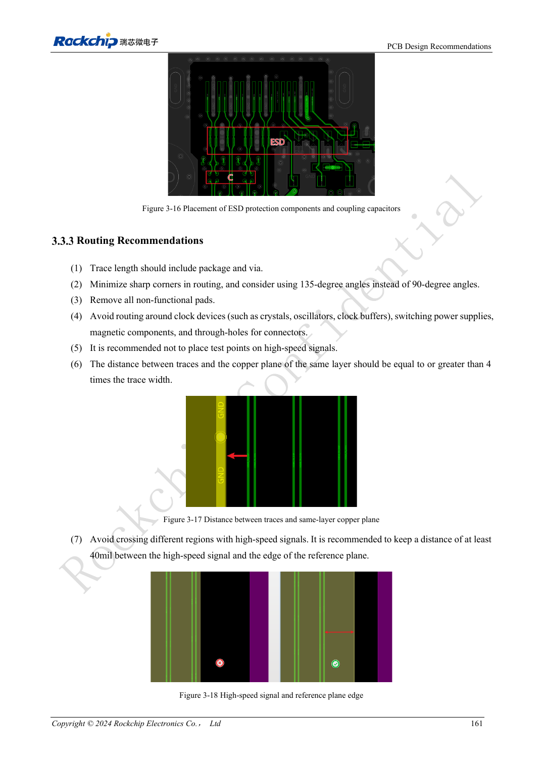
English original · PDF 180 · 3-18
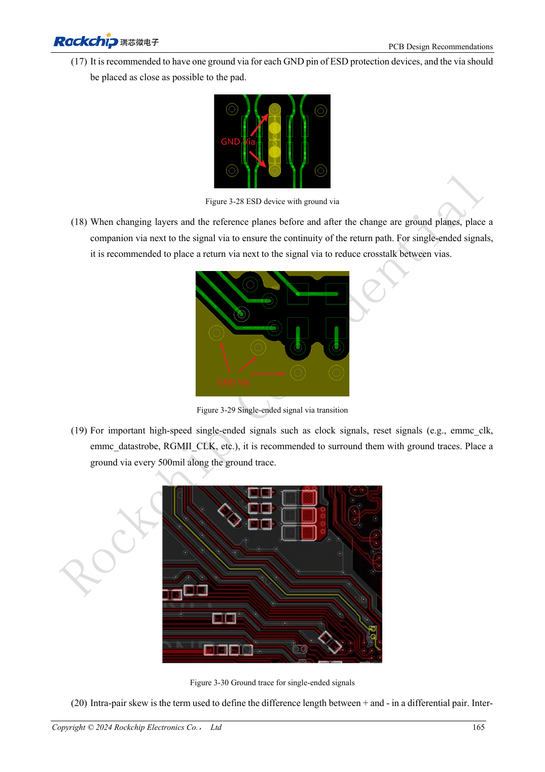
English original · PDF 184 · 3-29
ArmSoM development path
CM5 reduces repeated compute-core design on custom carriers; Sige5 provides a starting point for software and peripheral evaluation. Verify exposed interfaces, connector pins, voltages and image support in board documentation rather than inferring them from SoC features.