
This task-focused guide explains the source with key specifications, limitations and original figures. It is not a page-by-page translation or a complete pin/register manual. Vendor examples are not ArmSoM measurements. Check the actual board revision, schematic, SDK/BSP, kernel and drivers before applying them; no new hardware validation was performed for this article.
Primary source: Rockchip RK3568 Datasheet V1.2-20210601.pdf · PDF 62 pages.
Start with the workload, then allocate interfaces
RK3568 combines four Cortex-A55 cores, dedicated media engines and a broad set of embedded interfaces. Allocate networking, display, storage and inference resources together. ArmSoM documents identify Sige3 as an RK3568B2 board; this older RK3568 V1.2 datasheet is an architectural reference. Check the B2 revision, fitted memory and exposed interfaces against Sige3 documentation.
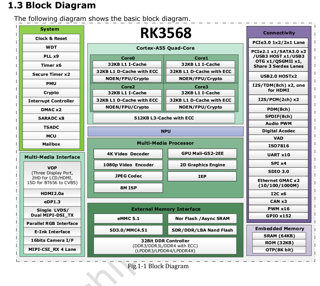
RK3568 vendor block diagram — Original English figure. Rockchip RK3568 Datasheet V1.2-20210601.pdf, PDF p. 19.
Specifications that guide the design
| Block | Source specification | Design implication |
|---|---|---|
| CPU | 4× Cortex-A55; ARMv8; Neon and TrustZone | Budget application, communication and media scheduling separately |
| NPU | Up to 1 TOPS; INT8/INT16/FP16/BFP16 | Check operators, quantization and toolchain support; TOPS does not predict frame rate |
| GPU | Mali-G52 1-Core-2EE; OpenGL ES 1.1/2.0/3.2, OpenCL 2.0, Vulkan 1.1 | Available APIs depend on the image and driver |
| Memory | 32-bit; DDR3/DDR3L/DDR4/LPDDR3/LPDDR4/LPDDR4X; up to 8GB addressing | Memory types are alternatives; the address limit is not a board’s fitted capacity |
| Video | H.264/H.265 decoding up to 4096×2304@60fps; encoding at 1920×1080@60fps | Codec limits do not establish concurrent multi-stream throughput |
| Camera | MIPI CSI as 1×4-lane or 2×2-lane; up to 2.5Gbps per lane | Match sensor, connector, clock, power and driver |
| Ethernet | 2 MACs; Gigabit RGMII or Fast Ethernet RMII | A MAC still needs a PHY, magnetics and suitable routing |
Maximum CPU/GPU frequencies remain TBD on PDF p. 56. A frequency advertised for another product must not be inserted as a conclusion of this datasheet. Some features also depend on product configuration and third-party licensing.
SATA, USB and PCIe are not additive totals
Pages 16–17 define three Multi-PHY resources. Draw the paths that must work simultaneously before selecting a board or designing a carrier.
| Resource | Alternative functions within that resource |
|---|---|
| Multi-PHY0 | USB3.0 OTG / SATA0 |
| Multi-PHY1 | USB3.0 Host / SATA1 / QSGMII/SGMII |
| Multi-PHY2 | PCIe2.1 / SATA2 / QSGMII/SGMII |
| Separate PCIe3.0 PHY | 2 lanes; controller arrangement as 1×x2 or 2×x1 |
A design needing fast USB, a SATA data disk and PCIe expansion must check the physical connection of each path and its device-tree PHY mode. An interface existing in the chip does not mean every combination is exposed on Sige3.
Three useful application directions
Equipment gateway and lightweight services. Separate acquisition, protocol conversion, buffering and the management interface. Validate packet loss, storage power-loss recovery and sustained writes before running several services together. Select field-bus transceivers and isolation for the installation.
Information displays and operator terminals. HDMI, MIPI DSI, LVDS, eDP, RGB and EBC offer several display paths. The source lists three simultaneous displays, but LVDS is unavailable in dual-MIPI mode. Resolution alone is insufficient: check timing, touch, rotation, planes and the rendering backend.
Compact edge vision. Test capture, resize, colour conversion, NPU inference and reporting as a pipeline. Successful PC-side export does not prove that every operator accelerates on the board. Measure end-to-end latency, CPU fallback and dropped frames rather than only one inference step.
Electrical and thermal boundaries
Page 56 requires GPIO configuration to match the actual supply. A matching connector shape does not make 1.8V and 3.3V signals interchangeable. The source lists 0–80℃ ambient operation; its thermal chapter requires junction temperature below 125℃. Ambient and junction temperatures are different quantities and do not establish an industrial rating for the assembled product.
Thermal-resistance figures use specified reference-PCB simulation/reference conditions. With an enclosure, expansion board and thermal pad, measure the hottest workload and throttling again. Include USB devices, storage and the display in the power budget.
A reproducible Sige3 evaluation
Record the board revision, image checksum, kernel, device tree, driver and application versions. Test cold boot, individual interfaces, combined load, operation after thermal stabilization and unexpected power-loss recovery. Sige3 is an RK3568B2 development starting point; its results do not automatically qualify a different RK3568 board.
Products and development resources
- Sige3 — Product · Documentation
Further reading
Datasheet series and original PDF
- RK3568 overview
- RK3568 package and pins: all 636 ball assignments
- RK3568 architecture: DDR, displays and shared PHYs
- RK3568 electrical and thermal guide: supplies, I/O and thermal resistance
- Download the complete original PDF
Other chip datasheets
These links support cross-platform reading; electrical conditions and pins are not interchangeable.