
This article uses the specified datasheet revision. Values are vendor specifications, not ArmSoM measurements; no new hardware validation was performed. Check the actual silicon revision, board schematic, SDK/BSP, kernel and drivers. The explanations and editable tables assist reading; consult the original PDF for the complete specification and bit definitions not expanded here.
RK3568 · Rockchip RK3568 Datasheet V1.2-20210601.pdf · PDF 7–19.
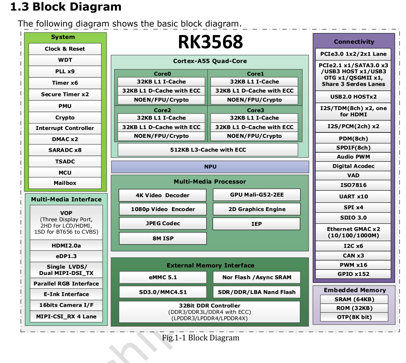
Original English figure, source PDF p. 19.
Compute, memory and boot
CPU, GPU and NPU are separate resources. NPU specifications do not directly determine model frame rate; Sige3 deployment needs model conversion, driver and bandwidth validation. Maximum DDR capacity is not fitted capacity.
| Item | Specification / source note |
|---|---|
| CPU | 4 × Cortex-A55 · Armv8-A · NEON |
| GPU | Mali-G52 · 1 core / 2 execution engines |
| NPU | 1 TOPS · INT8/INT16/FP16/BFP16 |
| DDR | 32 bit · ≤8 GB |
| DDR3/DDR3L/LPDDR3 | ≤2133 Mbit/s |
| DDR4/LPDDR4/LPDDR4X | ≤3200 Mbit/s |
| Ranks | DDR3/DDR3L/DDR4: 2; LPDDR3/LPDDR4/LPDDR4X: 4 |
| ECC | 8 bit · DDR3/DDR3L/DDR4 |
| eMMC | 5.1 · HS200 · command queue · 1/4/8 bit |
| NAND | 8 bit · 4 banks · ECC 70 bit / 1 KB · DDR clock ≤75 MHz |
| FSPI | 1/2/4 bit SDR · serial NOR/NAND/pSRAM/SRAM |
| SRAM | 64 KB + PMU 8 KB |
Codecs and image paths
| Item | Specification / source note |
|---|---|
| Decode | H.265 Main10 YUV420 / H.264 Main10 YUV400/420/422 / VP9 Profile 0/2: 4096×2304 @60 |
| Other decoding | VP8/VC-1/MPEG-4/2/1: 1920×1088 @60; H.263: 720×576 @60 |
| Encode | H.264 BP/MP/HP L4.2: 1920×1080 @60; H.265 MP L4.1: 1920×1080 @60 or 4096×4096 @10 (tile) |
| JPEG | Decode ≤8176×8176 / 76 Mpixel/s; encode ≤8192×8192 / 90 Mpixel/s |
| RGA | Input ≤8192×8192; output ≤4096×4096; scaling 1/16–16; rotation/mirror |
| MIPI CSI | 1 × 4 lanes or 2 × 2 lanes · ≤2.5 Gbit/s per lane |
| DVP | 8/10/12/16 bit · ≤150 MHz |
| ISP | ≤4096×2304; two-frame HDR |
| VICAP | 4 IDs; crop; NV16/NV12 |
Limits of three-display combinations
The three outputs have different ceilings; they cannot all be assigned the highest one. LVDS is unavailable in dual-MIPI mode. Check VOP routing, pixel clocks, pin sharing and software together.
| Item | Specification / source note |
|---|---|
| VOP | 2 cluster + 2 esmart + 2 smart; 4096×2304 / 2048×1536 / 1920×1080 @60 |
| HDMI | 1080p120 or 4096×2304 @60 · ≤10 bit · HDCP 1.4/2.2 |
| eDP | 1.3 · 4 lanes × 2.7 Gbit/s · 2560×1600 @60 · PSR |
| MIPI DSI | 2 × 4 lanes · ≤2.5 Gbit/s per lane; single 1080p60 / dual 2560×1440 @60 |
| RGB/BT.1120 | 1920×1080 @60 · ≤150 MHz |
| EBC | ≤2200×1650 · 16 bit · 16 gray levels · ≤256 frames per scan |
Shared PHYs and separate PCIe 3.0
Choose one function per shared PHY. The separate PCIe 3.0 lanes form one x2 or two x1 links, not both added together. Software cannot turn unrouted chip resources into board connectors.
| Item | Specification / source note |
|---|---|
| Multi-PHY0 | USB 3.0 OTG / SATA0 |
| Multi-PHY1 | USB 3.0 Host / SATA1 / QSGMII-SGMII |
| Multi-PHY2 | PCIe 2.1 / SATA2 / QSGMII-SGMII |
| PCIe 3.0 | 2 lanes · 2.5/5/8 Gbit/s; x2: RC/EP; x1 controller: RC |
| SATA | 3 controllers · 1.5/3/6 Gbit/s · AHCI 1.3.1 |
| QSGMII | 1 PCS; only 2 GMII controllers |
| Ethernet | 2 MAC · RGMII 10/100/1000 or RMII 10/100 |
| USB 2.0 Host | 2 · 480/12/1.5 Mbit/s |
Control, audio and sampling
| Item | Specification / source note |
|---|---|
| SPI | 4 controllers |
| I2C | 6 · 7/10-bit address · 100/400 kbit/s / 1 Mbit/s |
| UART | 10 · TX/RX FIFO 64 bytes · ≤4 Mbit/s; flow control UART0/1/3/4/5 |
| PWM | 16 × 32 bit; IR PWM3/7/11/15 |
| SARADC | 10 bit · 8 inputs · ≤1 MS/s |
| TSADC | 2 channels · ≤50 kS/s · −20…120 °C |
| OTP | 8 Kbit; 7 Kbit secure |
| I2S0/1 | 8 channels; I2S0 HDMI / I2S1 external |
| I2S2/3 | 2 channels |
| I2S | 16–32 bit · ≤192 kHz |
| PDM | 8 channels · 16–24 bit · ≤192 kHz |
| VAD | I2S/PDM input; amplitude detection; multi-mic storage |
Source issues and project checks
Allocate memory and PHYs, then check connectors and validate real workloads. The memory heading mentions LPDDR2 but its supported list omits it; support is not confirmed here. A Base Specification 3.0 reference in the PCIe 2.1 section does not establish 8 Gbit/s on that x1 PHY. CPU/GPU maxima remain TBD in the electrical table; check the actual SKU and BSP.
ArmSoM products and application limits
Sige3 uses RK3568B2. This article refers to the general RK3568 V1.2 datasheet and does not replace checking the B2 ordering variant, board revision and exposed interfaces.