
This article uses the specified datasheet revision. Values are vendor specifications, not ArmSoM measurements; no new hardware validation was performed. Check the actual silicon revision, board schematic, SDK/BSP, kernel and drivers. The explanations and editable tables assist reading; consult the original PDF for the complete specification and bit definitions not expanded here.
RK3528 · Rockchip RK3528 Datasheet V1.0-20230522.pdf · PDF 23–28.
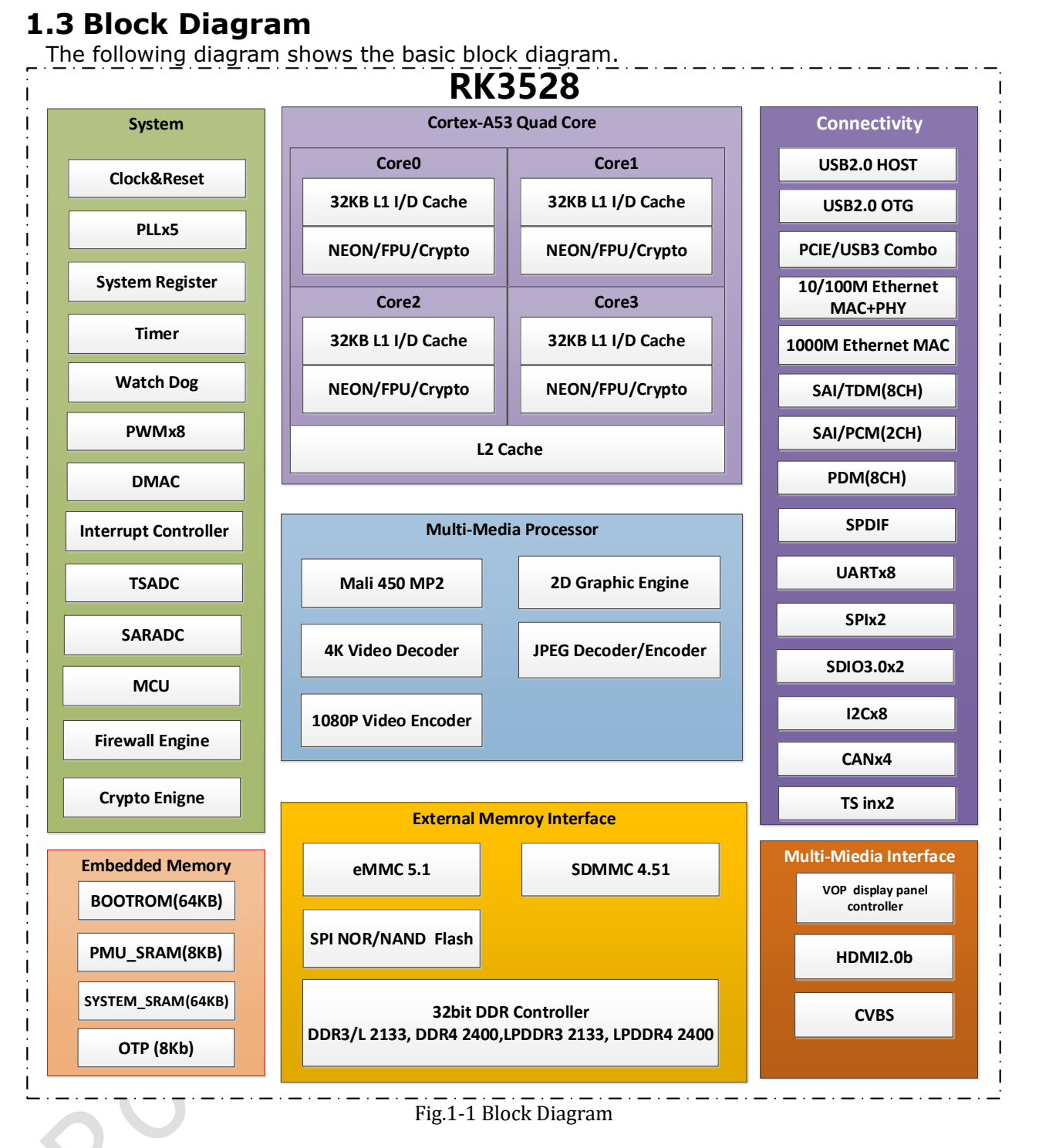
Original English figure, source PDF p. 14.
Stress limits and operating points
Absolute maxima are not regulator setpoints. Recommended Min/Typ/Max values do not replace sequencing, transient analysis or silicon-specific frequency/voltage tables. Measure at the chip during startup, idle and load transitions, not only at the regulator output.
Recommended supplies and clocks
PDF 23
| Rail / clock | Min | Typ | Max | Unit |
|---|---|---|---|---|
| CPU_DVDD | 0.81 | 0.90 | TBD | V |
| GPU_DVDD | 0.81 | 0.90 | TBD | V |
| LOGIC_DVDD | 0.81 | 0.90 | 0.99 | V |
| PMU_LOGIC_DVDD | 0.81 | 0.90 | 0.99 | V |
| PMU_PLL_AVDD1V8 DDR_PLL_AVDD1V8 |
1.62 | 1.8 | TBD | V |
| VCCIOi(i=0~4) | 1.62 3.0 |
1.8 3.3 |
1.98 3.465 |
V |
| PMUIO_VCC3V3 | 3.0 | 3.3 | 3.465 | V |
| HDMI_TX_AVDD1V8 | 1.62 | 1.8 | 1.98 | V |
| USB20_AVDD1V8 | 1.62 | 1.8 | 1.98 | V |
| USB20_AVDD3V3 | 3.0 | 3.3 | 3.6 | V |
| FEPHY_AVDD1V8 | 1.62 | 1.8 | 1.98 | V |
| FEPHY_AVDD3V3 | 2.97 | 3.3 | 3.63 | V |
| OTP_VCC1V8 | 1.62 | 1.8 | 1.98 | V |
| VDAC_AVDD1V8 | 1.62 | 1.8 | 1.98 | V |
| ACODEC_AVDD1V8 | 1.62 | 1.8 | 1.98 | V |
PDF 24
| Rail / clock | Min | Typ | Max | Unit |
|---|---|---|---|---|
| PCIE20_USB30_AVDD1V8 | 1.62 | 1.8 | 1.98 | V |
| SARADC_AVDD1V8 | 1.62 | 1.8 | 1.98 | V |
| DDR3 / DDR_VDDQ | 1.425 | 1.5 | 1.575 | V |
| DDR3L / DDR_VDDQ | 1.283 | 1.35 | 1.417 | V |
| LPDDR3 / DDR_VDDQ | 1.14 | 1.2 | 1.3 | V |
| DDR4 / DDR_VDDQ | 1.14 | 1.2 | 1.3 | V |
| LPDDR4 / DDR_VDDQ | 1.06 | 1.1 | 1.17 | V |
| LPDDR4X / DDR_VDDQL | 0.54 | 0.6 | 0.66 | V |
| CPU | NA | NA | TBD | GHz |
| GPU | NA | NA | TBD | MHz |
| TA | 0 | NA | 80 | ℃ |
GPIO levels and internal resistors
| Item | Specification / source note |
|---|---|
| 3.3 V I/O: VIL | −0.3…0.8 V |
| 3.3 V I/O: VIH | 2.0…VDDO+0.3 V |
| 3.3 V I/O: VOL | −0.3…0.4 V |
| 3.3 V I/O: VOH | 2.4…VDDO+0.3 V |
| 1.8 V I/O: VIL max | 0.35 × VDDO |
| 1.8 V I/O: VIH min | 0.65 × VDDO |
| 1.8 V I/O: VOH min | 1.4 V |
| Internal pulls | 16 / 26 / 43 kΩ (Min/Typ/Max) |
PLL and USB parameters
| Item | Specification / source note |
|---|---|
| PLL integer: Fin / Fvco / Fout | 10–800 / 475–1900 / 9–1900 MHz |
| PLL integer: lock | 1000 typ / 1500 max input-clock cycles |
| PLL fractional: Fin / Fvco / Fout | 1–1200 / 950–3800 / 19–3800 MHz |
| PLL fractional: lock | 250 typ / 500 max input-clock cycles |
| USB output resistance | 40.5 / 45 / 49.5 Ω |
| USB HS high | 360 / 400 / 440 mV |
| USB HS low | −40 / 0 / 40 mV |
| USB disconnect | 570 / 600 / 664 mV |
| USB squelch | 100 / NA / 150 mV |
Temperature and cooling limits
Thermal resistance is a vendor simulation on a specified PCB, not an ArmSoM measurement. Enclosure, copper area, airflow, heatsink and power distribution affect temperature rise. Sensor range is not ambient operating range.
| Item | Specification / source note |
|---|---|
| θJA / θJB / θJC | 22.8 / 9.3 / 6.87 °C/W |
| Thermal model | 4-layer PCB · 114.3 × 101.6 mm |
| Tj | Source requires below 125 °C |
| Ta | 0…80 °C |
| SARADC | 10 bit · ≤1 MS/s |
| TSADC | −40…125 °C · ±3 °C accuracy · 0.6 °C resolution |
Preserved source issues
Many RK3528 absolute maxima, CPU/GPU maximum voltages and frequencies, and the PLL supply maximum remain TBD. Do not substitute another chip’s values. The feature chapter gives 5 °C temperature resolution; the electrical table gives 0.6 °C and ±3 °C accuracy. Thermal guidance requires Tj below 125 °C, while the absolute-rating temperature row says NA; confirm these differences with the supplier.
The DAC’s 93 dB SNR and −84 dB THD use source conditions including 1 kHz, 48 kHz sampling and 600 Ω load, not a promise for every load.
ArmSoM products and application limits
Sige1 is the RK3528 product entry point. Chip capabilities do not mean every interface is exposed on the board; use the Sige1 documentation for connectors, voltages, images and pin assignments.