
Complete technical text from the V1.0 Chinese source (2023-06-20, 44 pages) and English source (2023-06-29, 43 pages), retaining the product version, glossary and all four chapters. Legal, audience, revision and contents pages are omitted. This describes the specified Rockchip EVB7, not ArmSoM product specifications or a current support commitment. No flashing, wiring or hardware testing was performed. Firmware upgrades may overwrite data: back up and verify firmware and board versions first. Never hot-plug the display or expansion board; observe the final chapter’s ESD and power precautions.
Source differences and issues: Chinese function summary and 3.8 specify one SATA port; English summary and both function tables say two. Source values are retained for checking against the actual board. The Chinese display specification is 1920×1080, English 1080×1920. Chinese has an extra 4.1 subheading. English figure 3-10/3-11/3-14 captions UART/VGA/RS484 are corrected to SATA/DP/RS485 using Chinese and the photographs; Aggreko housing is read as acrylic from Chinese. Chinese-only dual 4-lane DPHY / dual 3-Trio CPHY summary and the connector models in 2.4 are added. Table 3-1 says CDPHY in Chinese, DPHY in English; signal values match and are preserved. TBD denotes an unspecified source value, not an editorial placeholder. Original diagrams and interfaces contain English/Chinese labels, not fully localized artwork.
This guide mainly introduces the basic functions and hardware features, multi-function hardware configuration, and software debugging operation methods of RK3588 EVB7. It aims to help debuggers use RK3588 EVB7 be faster and more accurately, and be familiar with RK3588 chip development and application solutions.
Product version The product versions corresponding to this document are as follows:
| Product name | Product version |
|---|---|
RK3588 EVB7 |
RK_EVB7_RK3588_LP4XD200P232SD8_V11_20230428 |
Acronyms used in this document:
| Abbreviation | English meaning | Chinese meaning |
|---|---|---|
CPU |
Central Processing Unit | 中央处理器 |
NPU |
Neural Network Processing Unit | 神经网络处理器 |
VPU |
Video Processing Unit | 视频处理器 |
DDR |
Double Data Rate | 双倍速率同步动态随机存储器 |
eMMC |
Embedded Multi Media Card | 内嵌式多媒体存储卡 |
eDP |
Embedded DisplayPort | 嵌入式数码音视讯传输接口 |
HDMI |
High Definition Multimedia Interface | 高清晰度多媒体接口 |
I2C |
Inter-Integrated Circuit | 内部整合电路(两线式串行通讯总线) |
I2S |
Inter-IC Sound | 集成电路内置音频总线 |
PMIC |
Power Management IC | 电源管理芯片 |
LDO |
Low Drop Out Linear Regulator | 低压差线性稳压器 |
DCDC |
Direct Current to Direct Current | 直流电转直流电 |
CAN |
Controller Area Network | 控制器局域网络 |
SARADC |
Successive Approximation Register Analog to Digital Converter |
逐次逼近寄存器型模数转换器 |
UART |
Universal Asynchronous Receiver/ Transmitter | 通用异步收发传输器 |
JTAG |
Joint Test Action Group | 联合测试行为组织 |
PWM |
Pulse Width Modulation | 脉冲宽度调制 |
MIPI |
Mobile Industry Processor Interface | 移动产业处理器接口 |
LVDS |
Low-Voltage Differential Signaling | 低电压差分信号 |
PMIC |
Power Management IC | 电源管理芯片 |
PMU |
Power Management Unit | 电源管理单元 |
RK/Rockchip |
Rockchip Electronics Co.,Ltd. | 瑞芯微电子股份有限公司 |
USB |
Universal Serial Bus | 通用串行总线 |
SATA |
Serial Advanced Technology Attachment | 串行高级技术附件 |
PCIe |
Peripheral Component Interconnect Express | 外围组件快速互连 |
RGB |
Red,Green,Blue;RGB color mode is a color standard in industry |
红绿蓝,RGB 色彩模式, 是工业界的一 种颜色标准 |
VGA |
Video Graphics Array | 电脑显示视频图像标准接口 |
ADB |
Android Debug Bridge | 安卓调试桥 |
IR |
Infrared Radiation | 红外线 |
SPDIF |
Sony/Philips Digital Interface | 索尼/飞利浦数字音频接口 |
RTC |
Real-time clock | 实时时钟 |
RGMII |
Reduced Gigabit Media Independent Interface | 精简吉比特介质独立接口 |
WIFI |
Wireless Fidelity | 无线保真 |
CIF |
Camera Interface | 摄像头接口 |
1 System Introduction
1.1 RK3588 Introduction
RK3588 is a high-performance, low-power application processor chip. It integrates 4 Cortex-A76, 4 Cortex-A55 and independent NEON coprocessor. Suitable for ARM PC, edge computing, personal mobile Internet devices and other multimedia products. RK3588 has built-in a variety of powerful embedded hardware engines, providing excellent performance for high-end applications. It supports 8K@60fps H.265 and VP9 decoder, 8k@30fps H.264 decoder and 4K@60fps AV1 decoder; it also supports 8K@30fps H.264 and H.265 encoder, high quality JPEG encoder/decoder, dedicated image pre-processor and post-processor. RK3588 has a built-in 3D GPU that is fully compatible with OpenGL ES1.1/2.0/3.2, OpenCL 2.2 and Vulkan 1.2. The special 2D hardware engine with MMU will maximize the display performance and provide a smooth operating experience. RK3588 introduces a new generation of ISP with the largest 48M pixels completely based on hardware. It implements many algorithm accelerators, such as HDR, 3A, LSC, 3DNR, 2DNR, sharpening, defogging, fisheye correction, gamma correction, etc. The NPU embedded in RK3588 supports INT4/INT8/INT16/FP16 mixed operation, and the computing power is up to 6TOP. In addition, with its strong compatibility, network models based on a series of frameworks such as TensorFlow/MXNet/PyTorch/Caffe can be easily converted. RK3588 has high-performance 4-channel external memory interfaces (LPDDR4/LPDDR4X/LPDDR5), which can support systems with high memory bandwidth requirements, and also provides a complete set of peripheral interfaces to flexibly support various Class application.
1.2 RK3588 Chip Block Diagram
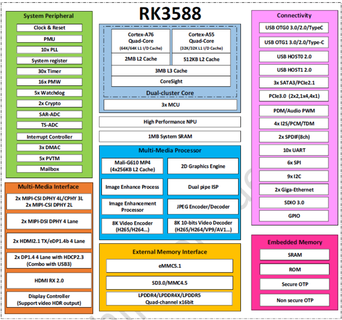
Figure 1-1 RK3588 Chip Block Diagram
1.3 System Framework
1.3.1 System Block Diagram
The RK3588 EVB7 system uses the RK3588 chip with the RK806-1 single PMIC power supply scheme. The storage uses a combination of LPDDR4X and eMMC. It supports various external interfaces such as 2xHDMI TX, 1xDP OUT, 1xHDMI RX, 2xMIPI TX, SATA, PCIe30x4, TYPEC, 2xRJ45, etc. The system supports a stable and feasible solution for mass production.The detailed system block diagram is as follows:
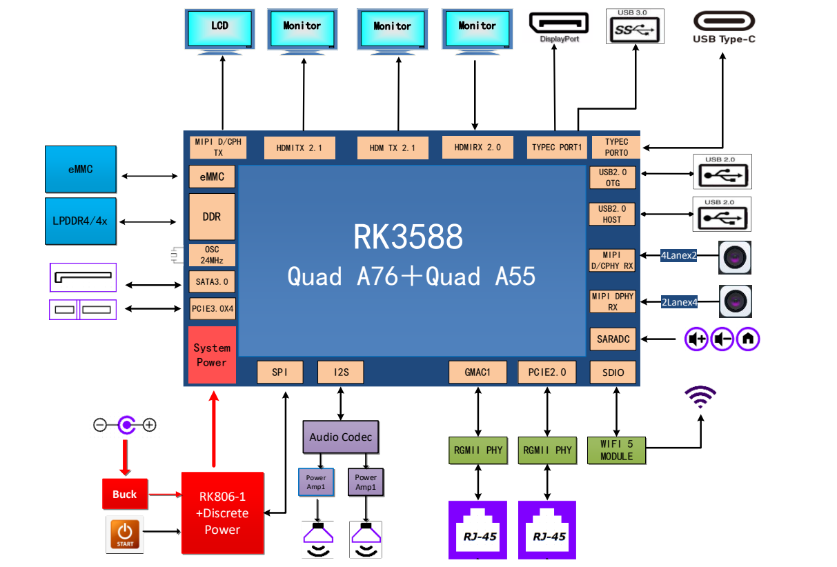
Figure 1-2 RK3588 EVB7 System Block Diagram
1.3.2 Function Summary
RK3588 EVB7 includes the following functions:
- DC Power: DC 12V adapter power supply interface
- TYPEC: One complete TYPEC interface, compatible with system firmware upgrade channel and DP1.4 output interface
- USB2.0 HOST1: one-way USB2.0 standard-A interface, can connect to mouse, U disk, USB HUB and other equipment
- USB2.0 OTG: one-way USB2.0 standard-A interface supports OTG, can connect to PC, mouse, U disk, USB HUB and other equipment
-
USB3.0 HOST: one-way USB3.0 standard-A interface, can connect to mouse, U disk, USB HUB and other equipment
-
MIPI DCPHY RX (Chinese-source addition): two 4-lane MIPI DPHY inputs or two 3-Trio MIPI CPHY inputs through an 80-pin connector.
- MIPI DPHY RX: Support two 4lane or four 2lane MIPI signal input, connected via 80pin connector. It supports camera function through ext-board RK_EVB_RK3588_EXTBOARD1_IMX415_V11_20211027
- HDMI2.1 OUT: Two HDMI2.1 OUT standard-A interfaces, a single channel can support up to 8K@60Hz output
- DP OUT: one DP OUT standard-A interface, a single channel can support up to 4K@60Hz output
- HDMI2.0 IN: one HMI IN standard-A interface, support up to 4K@60Hz video input
- MIPI DPHY0/1 TX: Support two 4lane MIPI signal output, access via FPC line
- Wi-Fi (2T2R MIMO): Wi-Fi model is AP6398, external SMA antenna, support wireless Internet function
- Ethernet: Support two channels RJ45 ports 10/100/1000M Ethernet;
- Audio Interface: Support speaker, earphone output sound, single MIC recording
- SATA3.0 Interface: Two 7pin SATA interface
- PCIe3.0 Interface: One standard PCIex4 interface, used to expand PCIe devices
- TF Card: supports TF card expansion, support SD3.0, MMC ver4.51
- UART Debug: User debugging to view the LOG information; support TYPEC and MINI USB interface;
- JTAG: JTAG debug interface of system;
- System Key: Include Reset, MASKROM, PWRON, V+/Recover, V-, MENU, ESC button;
- SPDIF: Support digital audio interface;
- RTC: Using HYM8563TS chip, can be powered by development board or button battery (CR1220-3V)
1.3.3 Functional Interface
Table 1-1 PCB Functional Interface Introduction Table
| Function | usable or not |
|---|---|
| LPDDR4x (total capacity 8GB) | YES |
| eMMC (total capacity 32GB) | YES |
| DC 12V Input | YES |
| TYPEC | YES |
| USB3.0 OTG (x1 Port) | YES |
| USB2.0 Host (x1 Port) | YES |
| USB2.0 OTG (x1 Port) | YES |
| MIPI D/CPHY RX | YES |
| MIPI DPHY RX | YES |
| HDMI2.0 RX | YES |
| HDMI2.1 OUT (2 Port) | YES |
| MIPI DPHY DSI TX1 (2x4lane) | YES |
| DP OUT | YES |
| BT&Wi-Fi (2x2 Wifi&BT5.0) | YES |
| 1000 Mbps Ethernet port 10M/100M/1000M (2 Port) | YES |
| Audio (SPK、MIC、Earphone) | YES |
| SATA3.0 Interface (2 Port) | YES |
| PCIe3.0 Interface (4Lane) | YES |
| UART Debug (TPYEC/MINI USB) | YES |
| JTAG Interface | YES |
| System Key | YES |
| Maskrom Key | YES |
1.3.4 Function Module Layout
EVB7 functional interface distribution diagram:
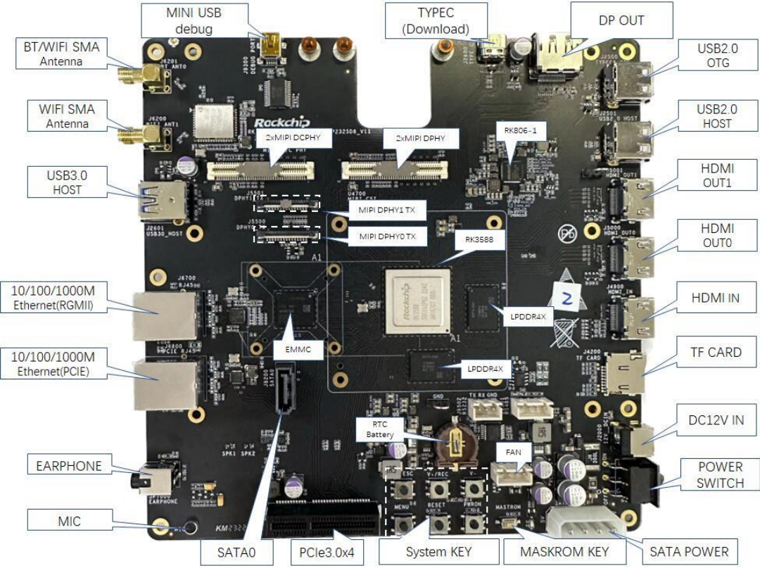
Figure 1-3 EVB7 Functional Interface Distribution Diagram (front)
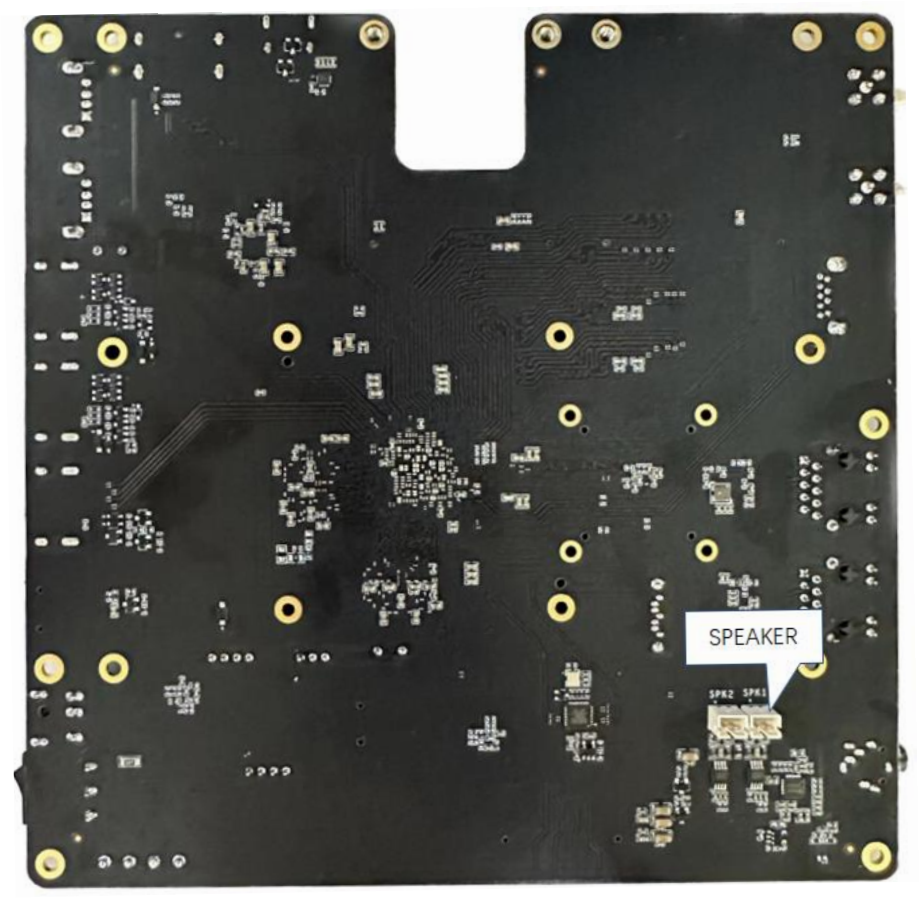
Figure 1-4 EVB7 Functional Interface Distribution Diagram (back)
1.4 Module
The RK3588 EVB7 kit includes the following items:
- RK3588 EVB7
- Power adapter, default specification: input 100V AC~240V AC, 50Hz; output 12V DC, 3A
- Display, specification: MIPI; size: 5.5 inches/vertical screen; resolution: 1080*1920
- One 2.4G/5G dual-band SMA male connector antennas
- IMX415 monocular camera module (EVB_RK3588_EXTBOARD1_IMX415_V11_20211027)
1.5 Power on and off and Standby
The EVB7 power on, power off and standby methods are introduced as follows:
- Power on: Use DC 12V power supply, turn on the main power switch; wait to enter the Android interface, it means that the default firmware has been successfully started.
- Power off: Press and hold the power button for 6 seconds to shut down the system.
- Standby: Press the power button, the system will enter the first-level standby state. When there is no USB OTG connection, and there is no other operation (such as key operation), and the software does not have a Wake_Lock source. After about 3s, it will switch from the first-level standby to the second-level standby state. Standby mode can be exited through the Power button.
1.6 Firmware Upgrade
1.6.1 USB Driver Installation
The driver needs to be installed before the EVB driver is upgraded. The following describes the driver installation process under Windows system. Find DriverAssitant_v5.1.1 in the provided tool folder, and click DriverInstall.exe to pop up the following interface. Click “Install Driver” and wait for the prompt to install the driver successfully. If the old driver has been installed, please click “Uninstall Driver “ and reinstall the driver.
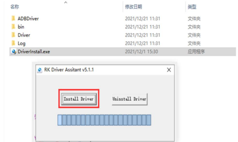
Figure 1-5 Schematic Diagram of Successful Driver Installation
1.6.2 Firmware Upgrade Method
There are two ways to upgrade RK3588 EVB7 firmware:
- Enter Loader upgrade mode: Before the system is powered on, SARADC_IN1 needs to be kept low, and the system will enter the Loader state. Specific steps are as follows:
1) Connect the TYPEC port to the PC, press and hold the V+/REC button on the mainboard.
2) EVB is powered by 12V. If it has been powered on, press the reset button.
3) After the programming tool shows that “a Loader device is found”, release the V+/REC button. In the red rectangular area of the tool, right-click and choose “Import Configuration”, then find the firmware path, and select the config file
4) The programming tool corresponds to selecting Loader, Parameter, Uboot and other files.
5) Click Execute to enter the upgrade state. The right side of the tool is the progress display bar, which displays the download progress and verification status.
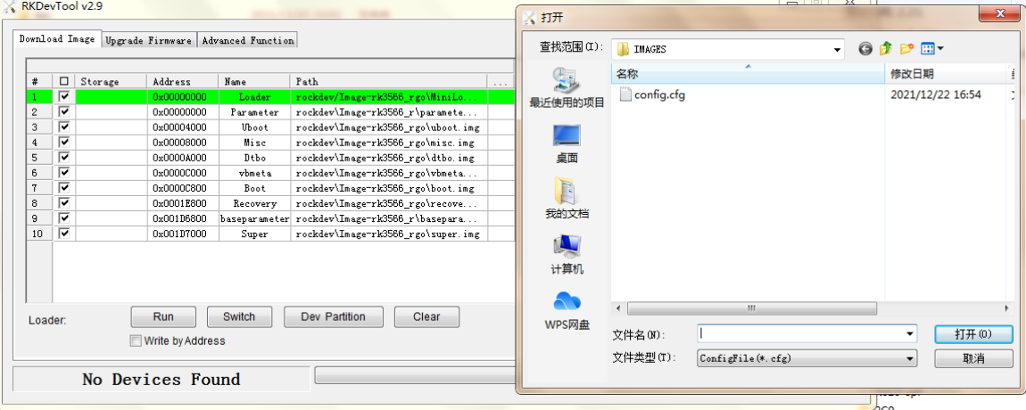
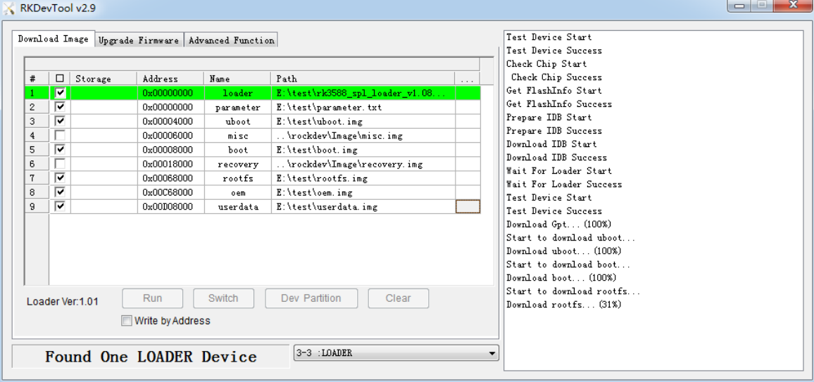
Figure 1-6 Schematic Diagram of Entering Loader Programming Mode
- Enter MASKROM upgrade mode: Before the system is powered on, SARADC_IN0 is low and enters the MASKROM state. Specific steps are as follows:
1) Connect the TYPEC port to the PC, press and hold the MASKROM button on the board.
2) EVB is powered by 12V. If it has been powered on, press the reset button.
3) After the programming tool shows that “a MASKROM device is found”, release the MASKROM button. In the red rectangular area of the tool, right-click and choose “Import Configuration”, then find the firmware path, and select the config.cfg file
4) The programming tool correspondingly selects Loader, Parameter, Uboot and other files.
5) Click Execute to enter the upgrade state. The right side of the tool is the progress display bar, which displays the download progress and verification status.
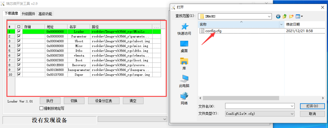
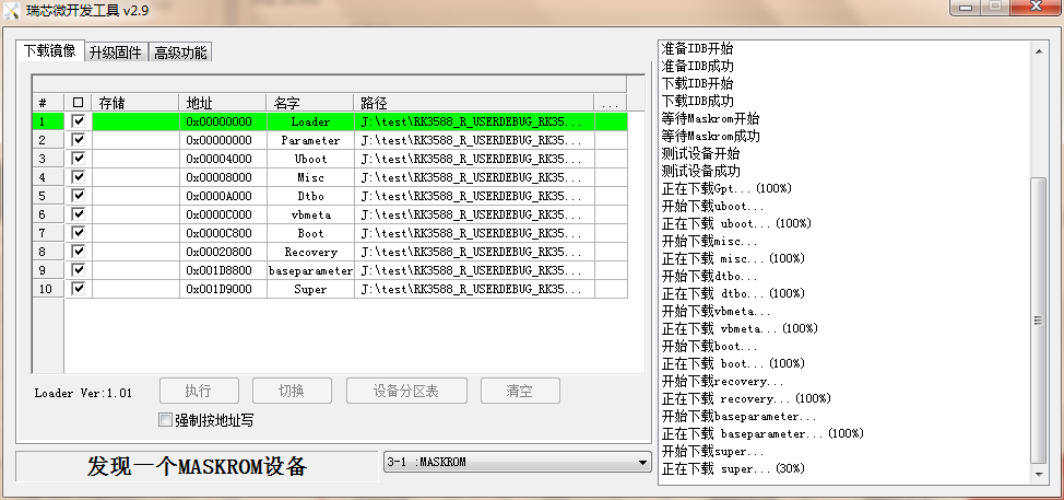
Figure 1-7 Schematic Diagram of Entering MASKROM Programming Mode
1.7 Serial Debugging
1.7.1 Serial Port Tool
Connect the MINI USB Debug debugging interface of the development board to the computer, and get the current port COM number in the device manager of the PC end.
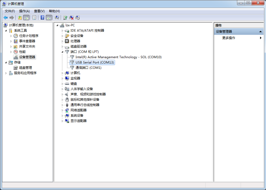
Figure 1-8 Get the Current Port COM Number
Open the serial port tool, under the “Quick Connect” interface, first select the serial port, then select the corresponding serial port number, change the baud rate to 1.5M (RK3588 supports 1.5M baud rate by default), and close the flow control at Serial, Finally, click the “Open” button to enter the serial port debugging interface.
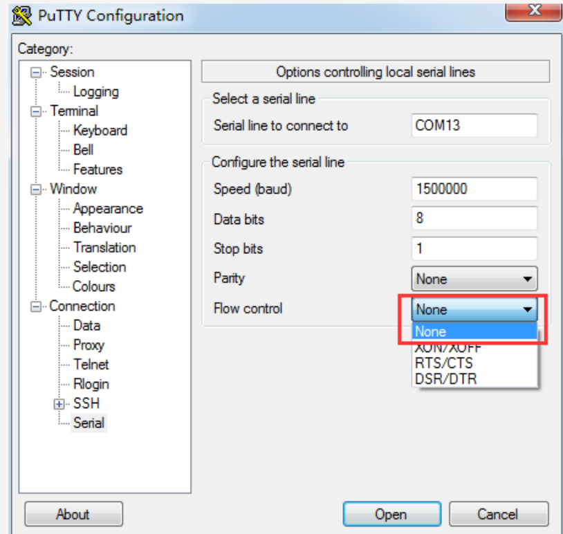
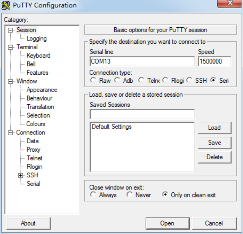
Figure 1-9 Serial Port Tool Configuration Interface
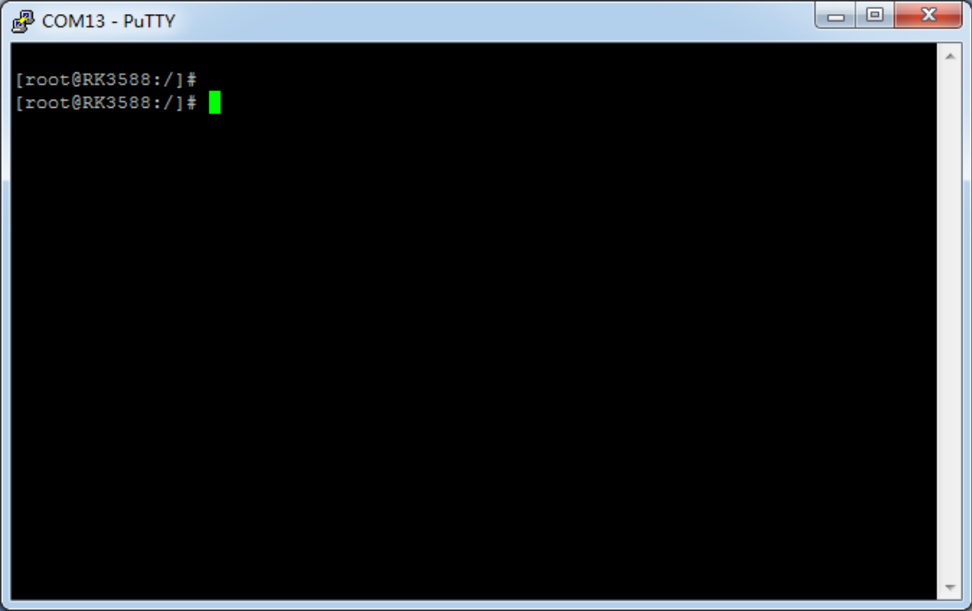
Figure 1-10 Serial Port Tool Debug Interface
1.7.2 ADB Debug
1) Ensure that the driver is installed successfully, and the PC is connected to the TYPE_C port on the same side as the power supply of the development board;
2) Power on the development board and boot into the system;
3) Open the adb tool on the PC side;
4) Type “adb shell” to enter adb debugging.
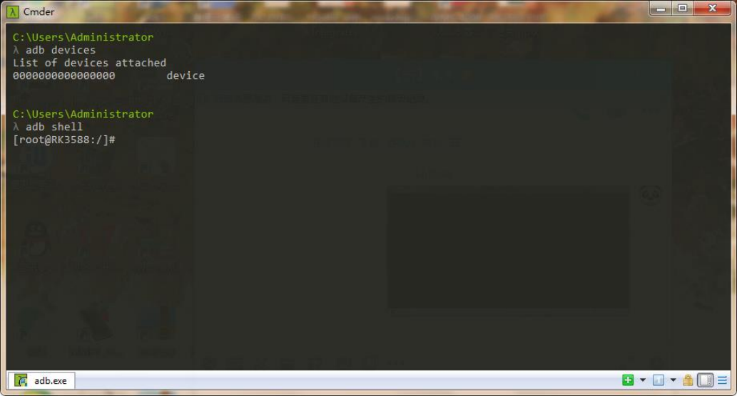
Figure 1-11 ADB Connection is Normal
2 Hardware Introduction
2.1 The Pictures
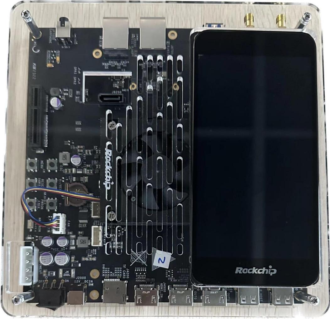
Figure 2-1 RK3588 EVB7 Picture
2.2 Power Block Diagram
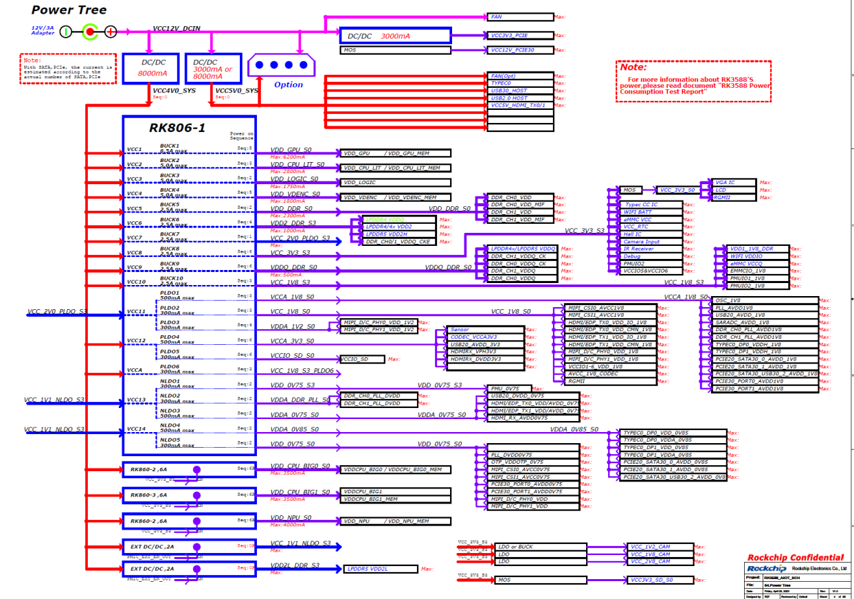
Figure 2-2 RK3588 EVB7 Block Diagram
2.3 I2C Address
The development board reserves a wealth of peripheral interfaces. The user debugging I2C peripherals will involve I2C channel multiplexing. Table 2-1 shows the I2C address and level values corresponding to the existing development board devices. Table 2-1 Correspondence Table of Peripheral Address and IO Level Value Mounted on I2C Channel
| I2C channel | Device | I2C address | Power domain |
|---|---|---|---|
I2C0_M2 |
RK860-2/RK860-3 |
0x42/0x43 |
3.3V |
I2C1_M2 |
RK860-2 |
0x42 |
3.3V |
I2C2_M4 |
MIPI DCPHY0/DCPHY1 |
TBD |
1.8V |
I2C3_M0 |
MIPI CSI0/MIPI CSI1 |
TBD |
1.8V |
I2C4_M1 |
STK3311-A/ICM-42607 |
TBD |
1.8V |
I2C5_M0 |
Touch Panel |
TBD |
3.3V |
I2C6_M0 |
HYM8563TS |
0xA3 |
3.3V |
I2C7_M0 |
ES8388 |
0x10 |
1.8V |
HDMITX0_I2C |
HDMI_TX0 |
TBD |
3.3V |
HDMITX1_I2C |
HDMI_TX1 |
TBD |
3.3V |
HDMIRX_I2C |
HDMI_RX |
TBD |
3.3V |
Note: When using the expansion board, make sure that the I2C address on the board does not conflict with the I2C address on the development board.
2.4 Extension Connector Information
In actual use, the user may make an expansion board. The model of the development board connector is as follows: U4600 and U4700 are vertical double-row 80PIN card sockets with 0.3mm pins and 0.8mm spacing. The dimensions are as follows:
Chinese-source connector models: board 61082-081402LF; mating expansion-board connector 61083-081402LF.
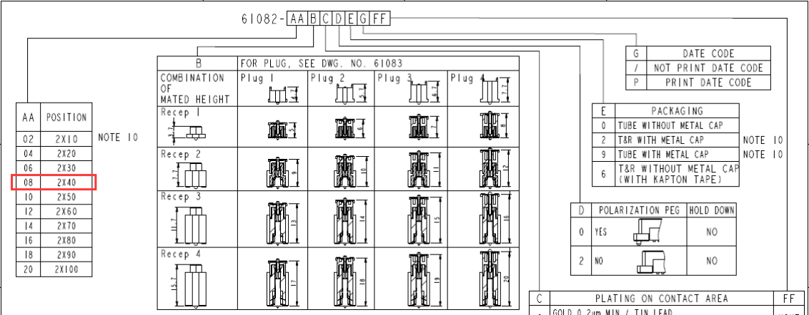
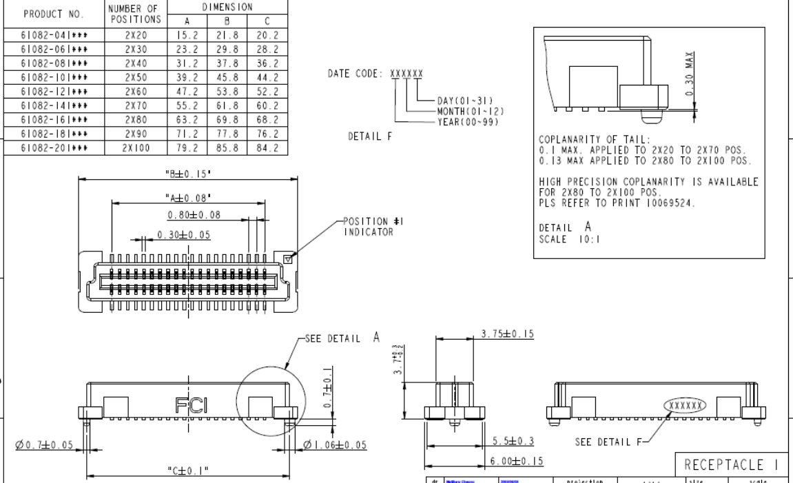
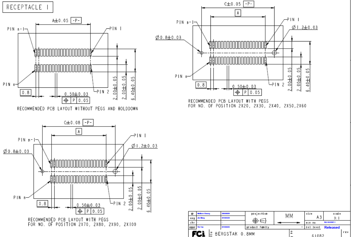
Figure 2-3 Pitch 0.8mm Vertical Double Row 80 PIN PCB Package
2.5 Reference Diagram
The reference diagram and PCB design information corresponding to the EVB7 are as follows:
- Reference diagram: RK_EVB7_RK3588_LP4XD200P232SD8_V11_20230428RZF.DSN
- PCB design: RK_EVB7_RK3588_LP4XD200P232SD8_V11_20230428YWQ_final.brd
3 Module Brief
3.1 Power Input
The power adapter inputs 12V/3A power, after passing the front-end buck converter power supply, the system power VCC4V0_SYS is obtained, and then the system voltage is provided to the PMIC power management chip, and different voltages are output for system use. Power adapter input port, front-end Buck converter and PMIC chip:
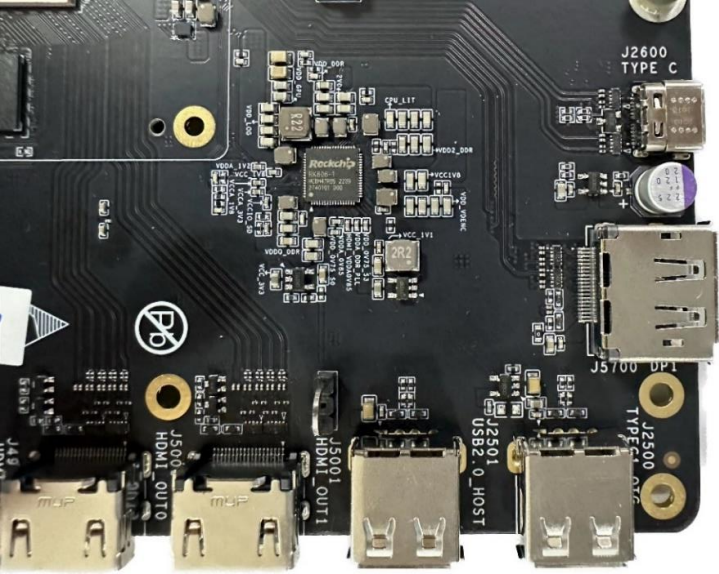
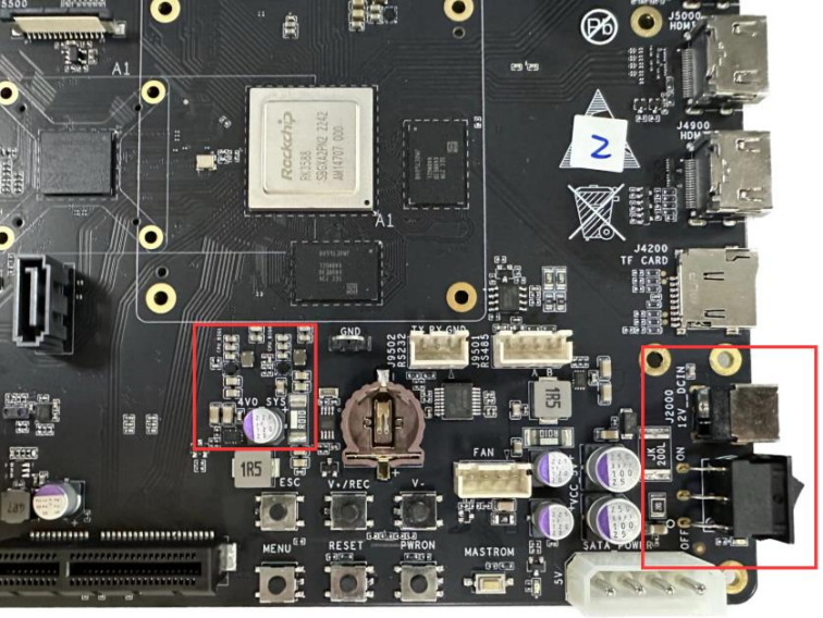
Figure 3-1 DC12V Input, Front-end Buck Converter and PMIC Chip
3.2 Memory
- eMMC: The storage type on the development board is eMMC FLASH, and the default capacity is 32GB;:
- DDR: The development board DDR adopts two pieces of 4GB LPDDR4x, with a total capacity of 8GB.
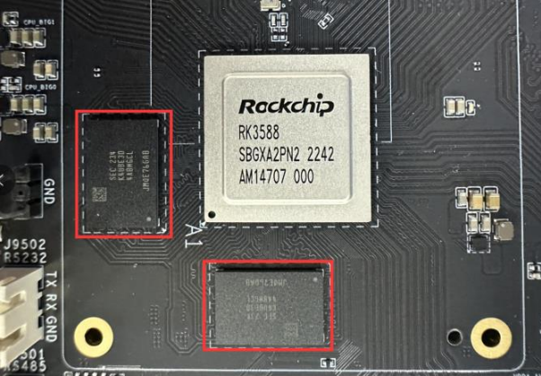
Figure 3-2 Location of LPDDR4x
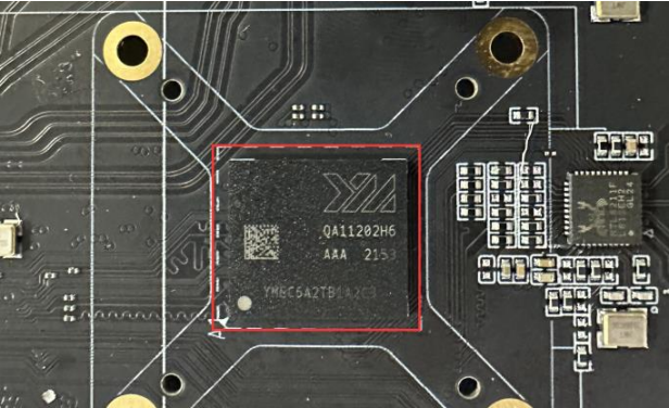
Figure 3-3 Location of eMMC The key position of EVB into MASKROM programming:
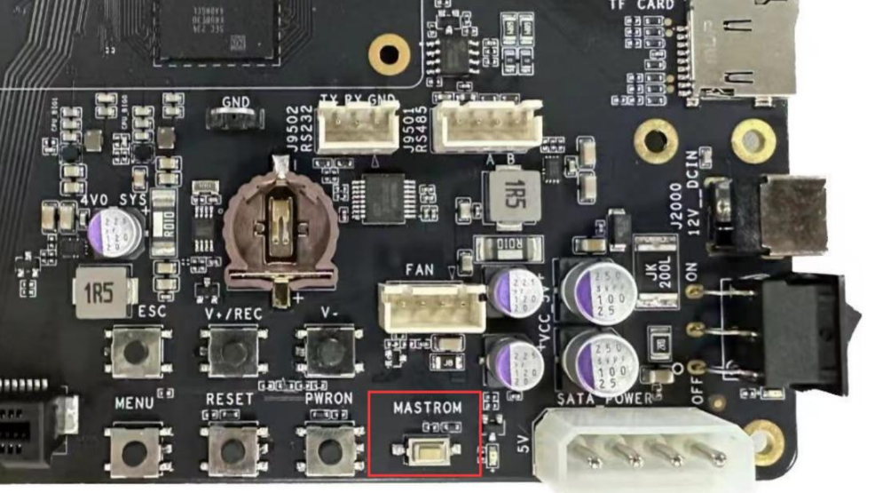
Figure 3-4 Key Position of EVB into MASKROM Programming
3.3 RTC Circuit
The RTC circuit adopts the HYM8563TS chip, which can be powered by the development board or its own button battery (not included by default, need to purchase a CR1220-3V button battery by user), to ensure that it can continue to provide accurate time even when the board is powered off, and communicate with master through the I2C signal.
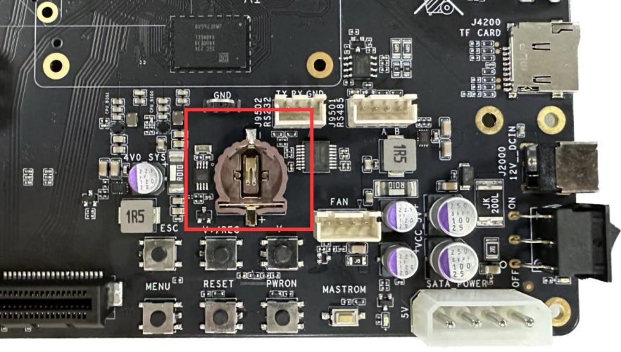
Figure 3-5 RTC Circuit
3.4 Key Input
The development board uses SARADC_IN1 as the RECOVER detection port, supports 12-bit resolution, and can enter the LOADER programming mode through the V+/REC button. In addition, the board also has a RESET button, which is convenient to reset and restart the machine through hardware; and other commonly used several Buttons: V+, V-, ESC, MENU, PWRON. The key positions are as follows:
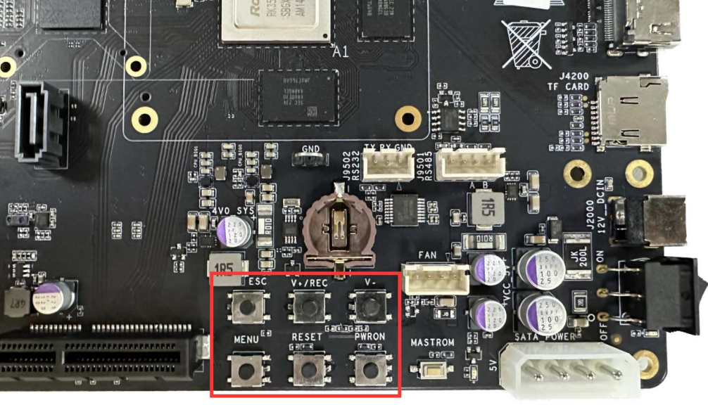
Figure 3-6 Key Position
3.5 SATA Power Socket
The SATA device power supply ports used by the development board output 12V/5V respectively.
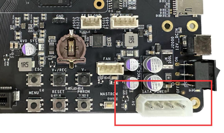
Figure 3-7 SATA Power 12V/5V Output
3.6 PCIe Socket
The development board uses a standard PCIe3.0 connector, which can be connected to an external PCIe card for communication.
- Working mode: End Point(EP) &Root Complex(RC).
- The link supports 4 lane data interfaces.
- The 100MHz clock is provided by the external clock chip AU5426.
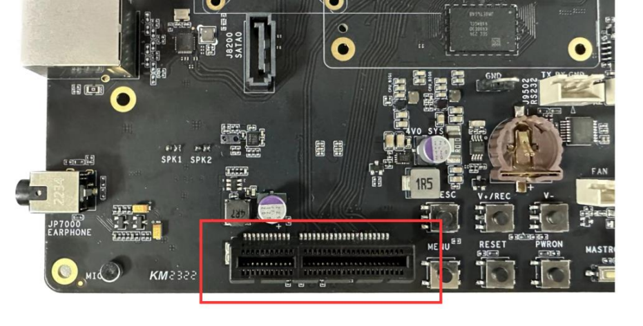
Figure 3-8 PCIex4 Socket
3.7 Ethernet Port
The development board supports two RJ45 ports, which can provide dual Gigabit Ethernet connection function.
The internal integrated Gigabit Ethernet MAC and PCIe2.0 are respectively used to connect with the external PHY chip. The PHY model is RTL8211F-CG/RTL8111HS. The characteristics are as follows:
- Compatible with IEEE802.3 standard, support full-duplex and half-duplex operation, support cross detection and self-adaptation.
- Support 10/100/1000M data rate.
- The interface adopts the combination of RJ45 interface with isolation transformer and indicator light.
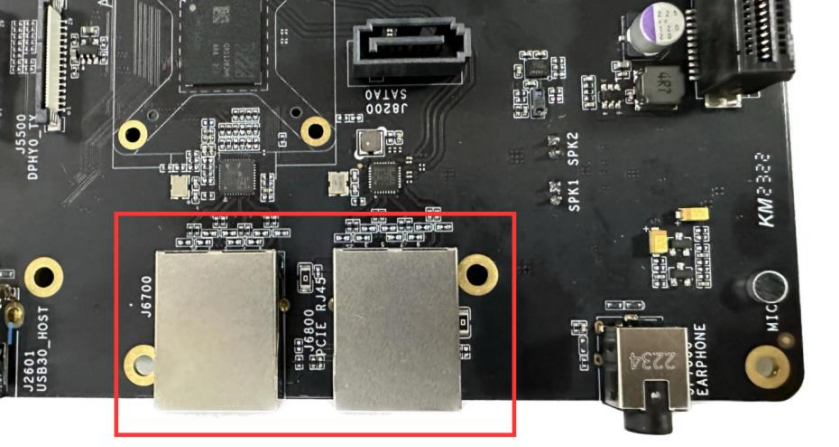
Figure 3-9 Gigabit Network Interface
3.8 SATA Interface
The development board provides one 7P SATA ports.
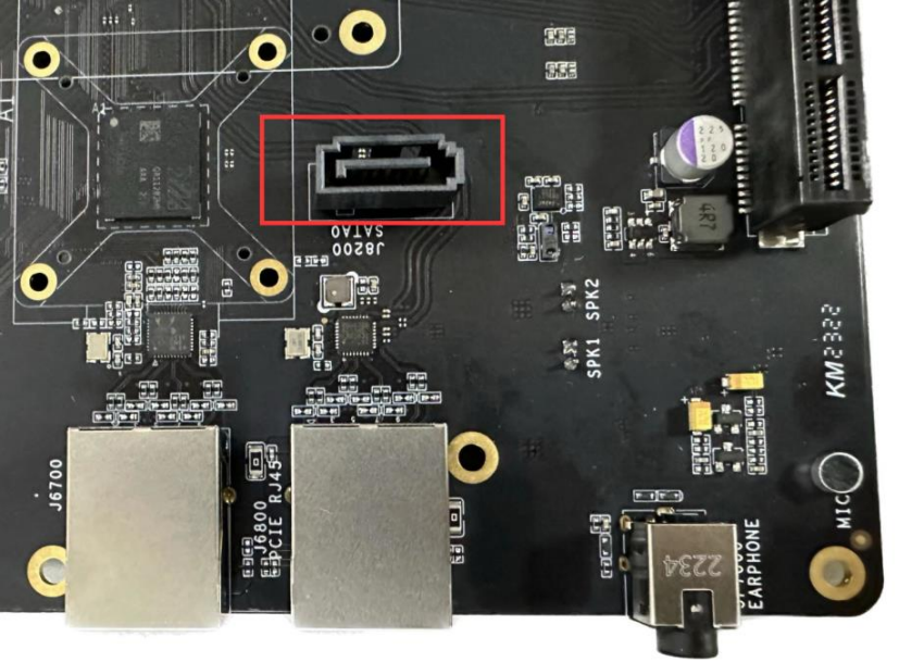
Figure 3-10 SATA Interface
3.9 DP Output
The development board supports DP interface video output, up to 4K@60 video output.
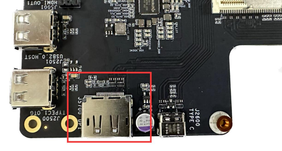
Figure 3-11 DP Video Output Interface
3.10 BT/WIFI Interface
The WIFI+BT module on the board adopts AMPAK AP6398S, and the characteristics are as follows:
- Support 2x2WIFI (2.4G and 5G, 802.11 a/b/g/n/ac), BT5.0 function, and 2 external SMA interface antennas.
- BT data adopts UART communication mode.
- BT voice is connected to the master I2S interface.
- WIFI data adopts SDIO interface. RK3588 EVB7 is equipped with one 2.4GHz/5GHz dual-mode antennas.
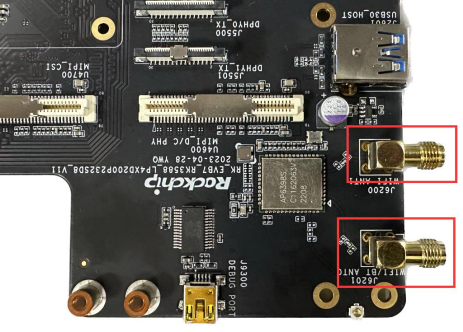
Figure 3-12 BT/WIFI Antenna Interface
3.11 Debug Interface
The development board has a built-in USB-to-UART chip, which supports a MINI USB debugging interface.
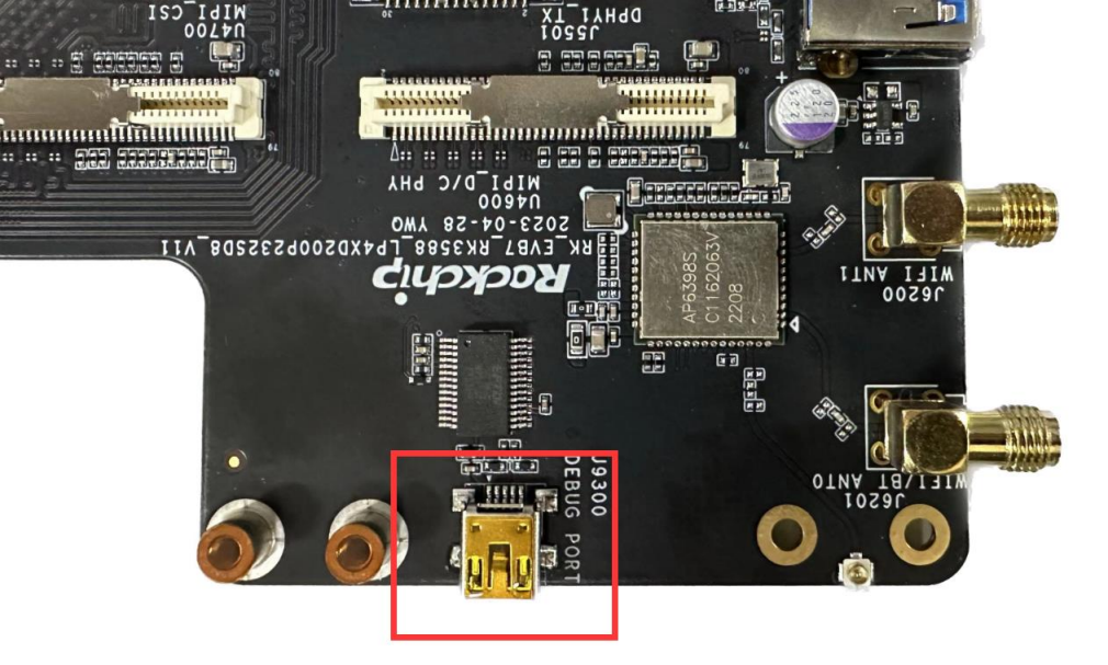
Figure 3-13 Debug Interface
3.12 RS485&RS232
The EVB board has reserved one RS485 and one RS232 interface.
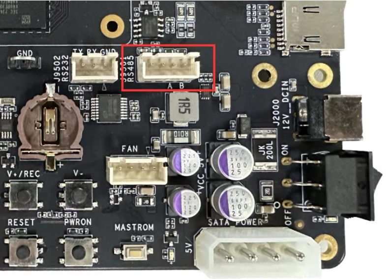
Figure 3-14 RS485 socket
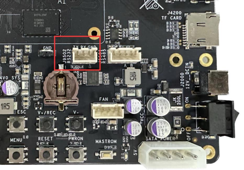
Figure 3-15 RS232 socket
3.13 MIPI D/CPHY Input Interface
The MIPI D/CPHY input interface adopts a vertical 80pin socket (61082-081402LF, see section 2.4 for specifications) with a pitch of 0.8mm, and supports dual MIPI D/CPHY interface input. It can support two-way 4Lane DPHY module input or two-way 3trio CPHY module input. MIPI DPHY/CPHY supports up to 4.5Gbps/Lane and 5.7Gbps/Trio respectively. The socket model for this 80pin socket is 61083-081402LF. Please refer to Chapter 2.4 for the package size specification. Expansion boards can be made as required.
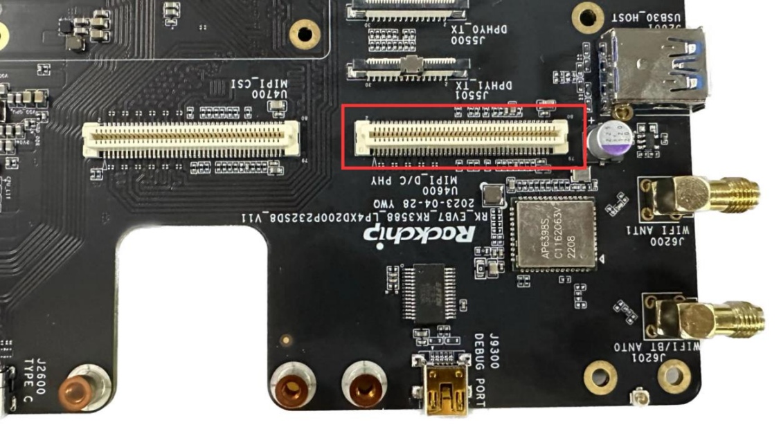
Figure 3-16 MIPI D/CPHY RX Input Interface
The MIPI D/CPHY_RX interface signal sequence is as follows: Table 3-1 MIPID/CPHY_RX Signal Definition Table
| Pin | DPHY (single) | DPHY (dual) | Pin |
|---|---|---|---|
1 |
GND |
GND |
2 |
3 |
MIPI_DPHY1_RX_D0N/MIPI_CPHY1_RX_TRIO0_A |
MIPI_DPHY0_RX_D0N/MIPI_CPHY0_RX_TRIO0_A |
4 |
5 |
MIPI_DPHY1_RX_D0P/MIPI_CPHY1_RX_TRIO0_B |
MIPI_DPHY0_RX_D0P/MIPI_CPHY0_RX_TRIO0_B |
6 |
7 |
GND |
GND |
8 |
9 |
MIPI_DPHY1_RX_D1N/MIPI_CPHY1_RX_TRIO0_C |
MIPI_DPHY0_RX_D1N/MIPI_CPHY0_RX_TRIO0_C |
10 |
11 |
MIPI_DPHY1_RX_D1P/MIPI_CPHY1_RX_TRIO1_A |
MIPI_DPHY0_RX_D1P/MIPI_CPHY0_RX_TRIO1_A |
12 |
13 |
GND |
GND |
14 |
15 |
MIPI_DPHY1_RX_CLKN/MIPI_CPHY1_RX_TRIO1_B |
MIPI_DPHY0_RX_CLKN/MIPI_CPHY0_RX_TRIO1_B |
16 |
17 |
MIPI_DPHY1_RX_CLKP/MIPI_CPHY1_RX_TRIO1_C |
MIPI_DPHY0_RX_CLKP/MIPI_CPHY0_RX_TRIO1_C |
18 |
19 |
GND |
GND |
20 |
21 |
MIPI_DPHY1_RX_D2N/MIPI_CPHY1_RX_TRIO2_A |
MIPI_DPHY0_RX_D2N/MIPI_CPHY0_RX_TRIO2_A |
22 |
23 |
MIPI_DPHY1_RX_D2P/MIPI_CPHY1_RX_TRIO2_B |
MIPI_DPHY0_RX_D2P/MIPI_CPHY0_RX_TRIO2_B |
24 |
25 |
GND |
GND |
26 |
27 |
MIPI_DPHY1_RX_D3N/MIPI_CPHY1_RX_TRIO2_C |
MIPI_DPHY0_RX_D3N/MIPI_CPHY0_RX_TRIO2_C |
28 |
29 |
MIPI_DPHY1_RX_D3P/NO_USE |
MIPI_DPHY0_RX_D3P/NO_USE |
30 |
31 |
GND |
GND |
32 |
33 |
NC |
NC |
34 |
35 |
NC |
NC |
36 |
37 |
GND |
GND |
38 |
39 |
MIPI_CAM1_CLKOUT |
MIPI_CAM2_CLKOUT |
40 |
41 |
NC |
NC |
42 |
43 |
GND |
GND |
44 |
45 |
I2C2_SDA_M4_MIPI |
I2C2_SDA_M4_MIPI |
46 |
47 |
I2C2_SCL_M4_MIPI |
I2C2_SCL_M4_MIPI |
48 |
49 |
NC |
NC |
50 |
51 |
MIPI_CAM1_PDN_L |
MIPI_CAM2_PDN_L |
52 |
53 |
NC |
NC |
54 |
55 |
NC |
NC |
56 |
57 |
MIPI_DPHY_FSYNC |
MIPI_DPHY_FSYNC |
58 |
59 |
MIPI_DPHY_HSYNC/PWM15_M2 |
MIPI_DPHY_HSYNC |
60 |
61 |
VCC_1V8_S3 |
VCC_3V3_S3 |
62 |
63 |
NC |
NC |
64 |
65 |
MIPI_CAM1_PWREN_H |
MIPI_CAM2_PWREN_H |
66 |
67 |
IRC_AIN |
NC |
68 |
69 |
IRC_BIN |
NC |
70 |
71 |
NC |
NC |
72 |
73 |
NC |
NC |
74 |
75 |
GND |
GND |
76 |
77 |
VCC_5V0 |
GND |
78 |
79 |
VCC_5V0 |
VCC12V_DCIN |
80 |
3.14 MIPI DPHY Input Interface
The MIPI DPHY input interface adopts a vertical 80pin socket with a pitch of 0.8mm (61082-081402LF, see section 2.4 for specifications). It can support two 4Lane MIPI DPHY module inputs or four 2Lane MIPI DPHY signal inputs. MIPI DPHY supports up to 2.5Gbps/Lane respectively. Together with MIPI D/CPHY, it can form a maximum of 6 module inputs. The socket model for this 80pin socket is 61083-081402LF. Please refer to Chapter 2.4 for the package size specification.
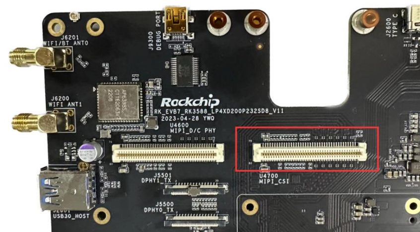
Figure 3-17 MIPI DPHY Video Input Interface Table 3-2 MIPI DPHY_RX Signal Definition Table
| Pin | DPHY (single) | DPHY (dual) | Pin |
|---|---|---|---|
1 |
GND |
GND |
2 |
3 |
MIPI_CSI0_RX_D0N |
MIPI_CSI1_RX_D0N |
4 |
5 |
MIPI_CSI0_RX_D0P |
MIPI_CSI1_RX_D0P |
6 |
7 |
GND |
GND |
8 |
9 |
MIPI_CSI0_RX_D1N |
MIPI_CSI1_RX_D1N |
10 |
11 |
MIPI_CSI0_RX_D1P |
MIPI_CSI1_RX_D1P |
12 |
13 |
GND |
GND |
14 |
15 |
MIPI_CSI0_RX_CLK0N |
MIPI_CSI1_RX_CLK0N |
16 |
17 |
MIPI_CSI0_RX_CLK0P |
MIPI_CSI1_RX_CLK0P |
18 |
19 |
GND |
GND |
20 |
21 |
MIPI_CSI0_RX_D2N |
MIPI_CSI1_RX_D2N |
22 |
23 |
MIPI_CSI0_RX_D2P |
MIPI_CSI1_RX_D2P |
24 |
25 |
GND |
GND |
26 |
27 |
MIPI_CSI0_RX_D3N |
MIPI_CSI1_RX_D3N |
28 |
29 |
MIPI_CSI0_RX_D3P |
MIPI_CSI1_RX_D3P |
30 |
31 |
GND |
GND |
32 |
33 |
MIPI_CSI0_RX_CLK1N |
MIPI_CSI1_RX_CLK1N |
34 |
35 |
MIPI_CSI0_RX_CLK1P |
MIPI_CSI1_RX_CLK1P |
36 |
37 |
GND |
GND |
38 |
39 |
MIPI_CAM3_CLKOUT |
MIPI_CAM4_CLKOUT |
40 |
41 |
NC |
NC |
42 |
43 |
GND |
GND |
44 |
45 |
I2C3_SDA_M0_MIPI |
I2C3_SDA_M0_MIPI |
46 |
47 |
I2C3_SCL_M0_MIPI |
I2C3_SCL_M0_MIPI |
48 |
49 |
NC |
NC |
50 |
51 |
MIPI_CAM3_PDN_L |
MIPI_CAM5_PDN_L |
52 |
53 |
NC |
NC |
54 |
55 |
MIPI_CAM4_PDN_L |
MIPI_CAM6_PDN_L |
56 |
57 |
MIPI_DPHY_FSYNC |
MIPI_DPHY_FSYNC |
58 |
59 |
MIPI_DPHY_HSYNC/PWM15_M2 |
MIPI_DPHY_HSYNC |
60 |
61 |
VCC_1V8_S3 |
VCC_3V3_S3 |
62 |
63 |
NC |
NC |
64 |
65 |
MIPI_CAM3/4_PWREN_H |
MIPI_CAM5/6_PWREN_H |
66 |
67 |
IRC_AIN |
NC |
68 |
69 |
IRC_BIN |
NC |
70 |
71 |
NC |
NC |
72 |
73 |
NC |
NC |
74 |
75 |
GND |
GND |
76 |
77 |
VCC_5V0 |
GND |
78 |
79 |
VCC_5V0 |
VCC12V_DCIN |
80 |
3.15 TYPEC Interface
The development board supports a complete TYPEC interface and supports the following functions:
- TYPEC0_USB20_OTG in this interface can be used to download firmware
- Support TYPEC function
- Support DP1.4 output
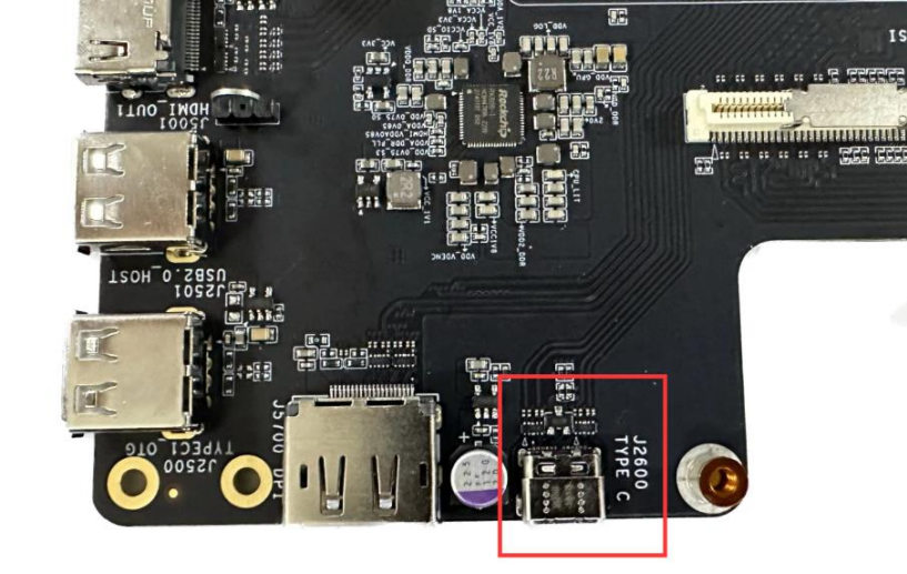
Figure 3-18 TYPEC Interface
3.16 USB3.0 Interface
The development board supports one USB3.0 OTG interface; the interface is a standard A port, which is convenient for developers to access USB3.0 U disk and other USB3.0 devices.
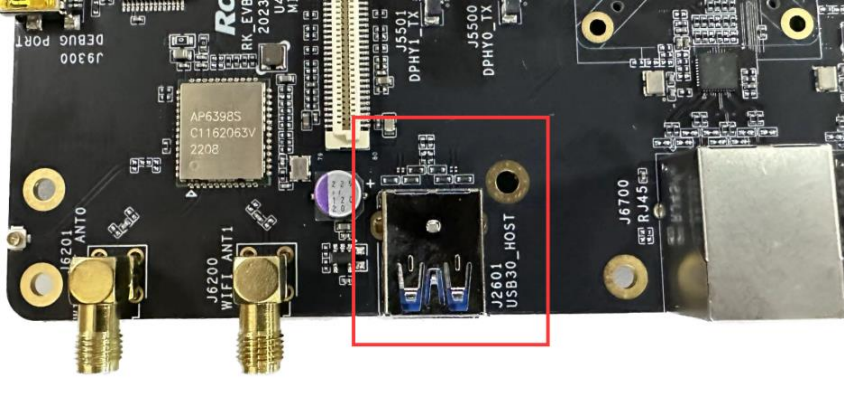
Figure 3-19 USB3.0 OTG Interface
3.17 USB2.0 OTG/Host Interface
The development board supports one USB2.0 HOST and one USB2.0 OTG, support the connection of USB devices, such as mouse, U disk, and Bluetooth.
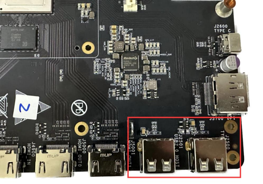
Figure 3-20 USB2.0 Interface
3.18 HDMI Output Interface
The development board supports two HDMI standard A output interfaces, up to HDMI2.1, and up to 8K@60fps video output.
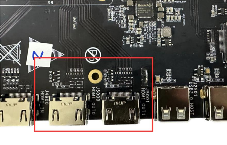
Figure 3-21 HDMI TX Interface
3.19 HDMI Input Interface
The development board supports one HDMI input interface, supports HDMI2.0 video input, up to 4K60fps video input.
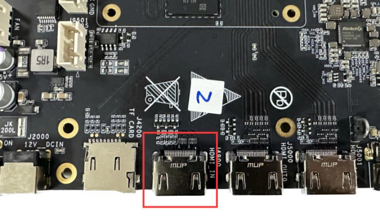
Figure 3-22 HDMI RX Interface
3.20 Fan Power Connector
The development board reserves a fan interface, supports 12V/5V fans, and supports adjustable speed. The development board equip with a 12V fan. The interface line sequence from left to right is GND, 12V, SENSOR, CONTROL.
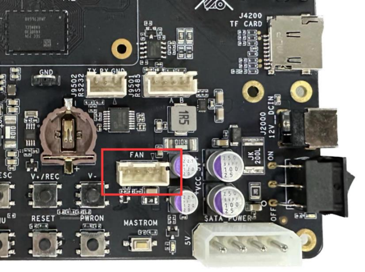
Figure 3-23 Fan Power Interface
3.21 Sensor Module Expansion
The development board is equipped with an IMX415 module, which can support up to 800W pixels.
- Support automatic white balance, 3D noise reduction, HDR;
- Support RAW10/RAW12 data output;
- Integrated IRCUT switching circuit, which can control the sensor module day and night mode;
- One set of 24pin MIPI interface is reserved on the module, which can be extended to stereo vision application as needed.
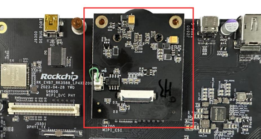
Figure 3-24 IMX415 Module Board The IMX415 module expansion interface signal sequence is as follows: Table 3-3 IMX415 Module Expansion Interface Signal Definition Table
| Pin | DPHY |
|---|---|
1 |
GND |
2 |
GND |
3 |
NC |
4 |
MIPI_DCPHY1_RX_RST_L |
5 |
I2C5_SDA_M0_MIPI |
6 |
I2C5_SCL_M0_MIPI |
7 |
GND |
8 |
GND |
9 |
MIPI_DPHY1_RX_D0N |
10 |
MIPI_DPHY1_RX_D0P |
11 |
MIPI_DPHY1_RX_D1N |
12 |
MIPI_DPHY1_RX_D1P |
13 |
MIPI_DPHY1_RX_D2N |
14 |
MIPI_DPHY1_RX_D2P |
15 |
MIPI_DPHY1_RX_D3N |
16 |
MIPI_DPHY1_RX_D3P |
17 |
GND |
18 |
MIPI_DPHY1_RX_CLKN |
19 |
MIPI_DPHY1_RX_CLKP |
20 |
GND |
21 |
MIPI_CAM2_CLKOUT |
22 |
VCC_3V3_O |
23 |
VCC_3V3_D |
24 |
VCC_3V3_A |
3.22 Speaker Interface
The development board reserves 2 speaker ports, and two general speakers are pre-installed in the acrylic housing.
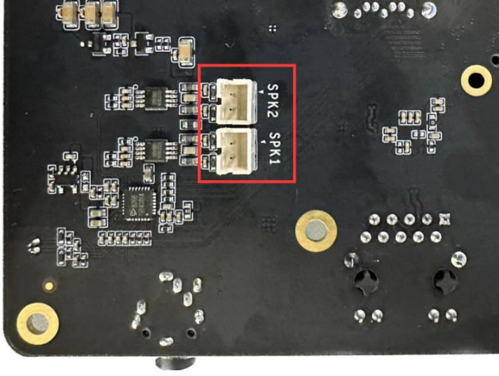
Figure 3-25 SPK Socket
4 Precautions
RK3588 EVB7 is suitable for laboratory or engineering environment, please read the following precautions before operation:
- Under no circumstances can the screen interface and expansion board be hot-swapped.
- Before unpacking and installing the development board, take necessary anti-static measures to avoid electrostatic discharge (ESD) damage to the development board hardware.
- When holding the development board, please hold the edge of the development board, and do not touch the exposed metal parts of the development board, so as to avoid damage to the components of the development board caused by static electricity.
- Please place the development board on a dry surface to keep them away from heat sources, electromagnetic interference sources and radiation sources, electromagnetic radiation sensitive equipment (such as medical equipment), etc.