This ArmSoM platform reference documents the RK806 IC; it does not establish compatibility with a particular ArmSoM board. Check the exact RK806 variant, schematic, rails and BSP. Application circuits and performance data are Rockchip examples, not ArmSoM hardware tests. No SDK/kernel version is specified. Source: the English122-page RK806 Rev1.3 PDF dated2023-10-19 (cover:Oct.2023). All33 figures are independently cropped English originals. Cover, revision-history and nontechnical legal/contact matter are omitted; technical conditions and source discrepancies are retained.
1.1 Overview
RK806 is a complex power-management IC that provides a complete solution with few external components. Ten synchronous step-down DC-DC converters use ripple-based control for fast load-transient response. Their output voltages can change dynamically with processor operating state to maximize efficiency; most channels are configured over I2C or SPI. Soft start reduces inrush current. The2MHz switching frequency and control method reduce external inductance/capacitance. Six LDO channels accept inputs down to2V for conversion efficiency; five additional NMOS LDOs are integrated. All LDO output voltages are configurable over I2C/SPI. OTP-based power-up/down sequencing is configurable for customized sequences. Two RK806 devices can cooperate as master/slave with synchronized power-up/down. Package: QFN68,7.0×7.0mm,0.35mm pitch.
1.2 Features
Input range2.7–5.5V; low standby current10uA. Every listed output range is0.5–3.4V. BUCK1:6.5A maximum; BUCK2/3/4:5A; BUCK5/6/7/8/9/10:3A, all with very fast transient response. NLDO1/2/5:300mA; NLDO3/4:500mA; PLDO1/4:500mA; PLDO2/3/5:300mA; VCCIO:300mA. OTP programs sequencing and voltage. Dual-PMIC cooperation and I2C/SPI communication are supported;7×7mm QFN68 package.
1.3 Block diagram
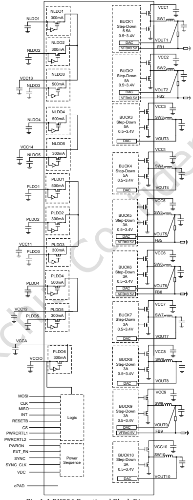
Fig.1-1 Functional block diagram — English original, Rev1.3, PDF page 9.
1.4 Typical applications
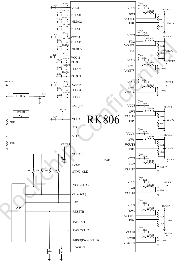
Single RK806 application — English original, Rev1.3, PDF page 10.
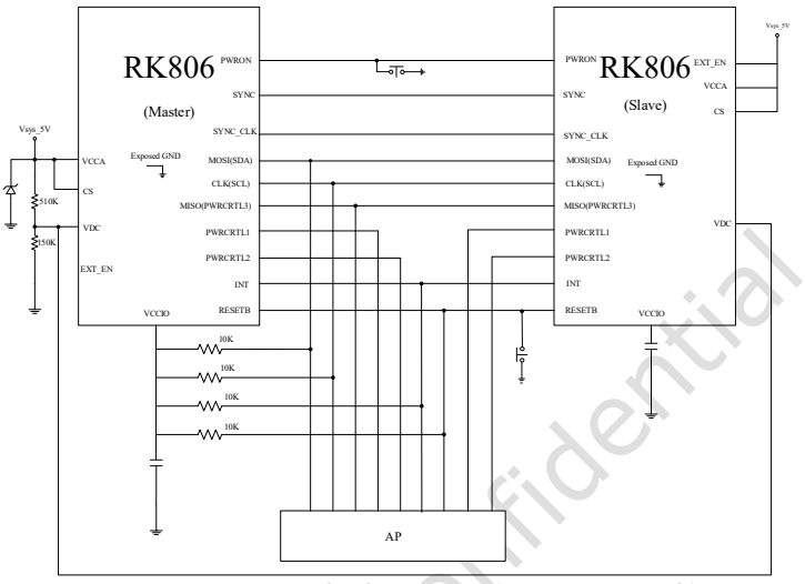
Two RK806, I2C — English original, Rev1.3, PDF page 11.
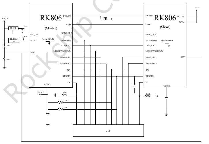
Two RK806, SPI — English original, Rev1.3, PDF page 11.
RK806-1/-2/-3 are RoHS QFN68(7×7), supplied2000 pieces per tape and5 tapes per box on reels. Marking: Rockchip brand; RKXXXX chip name; ABC subcontractor; XXXXXX die lot; DEFG date; NXXXXXX FXX OSAT sub-lot. The three marking illustrations identify pin1. Moisture sensitivity MSL3; lead finish/pin material Sn. Coplanarity applies to leads, corner leads and die-attach pad. Dimension b applies to metallized terminals, measured0.15–0.30mm from the tip, excluding any optional radius at the other end.
| Orderable device |
RoHS |
Package |
Packing |
| RK806-1 |
RoHS |
QFN68 (7×7) |
2000 pcs/tape;5 tapes/box;reels |
| RK806-2 |
RoHS |
QFN68 (7×7) |
2000 pcs/tape;5 tapes/box;reels |
| RK806-3 |
RoHS |
QFN68 (7×7) |
2000 pcs/tape;5 tapes/box;reels |
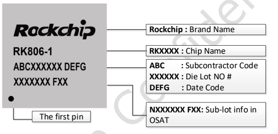
RK806-1 top marking — English original, Rev1.3, PDF page 12.
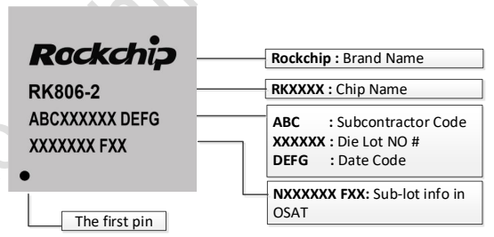
RK806-2 top marking — English original, Rev1.3, PDF page 12.
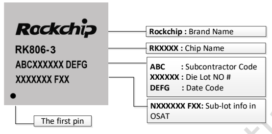
RK806-3 top marking — English original, Rev1.3, PDF page 13.
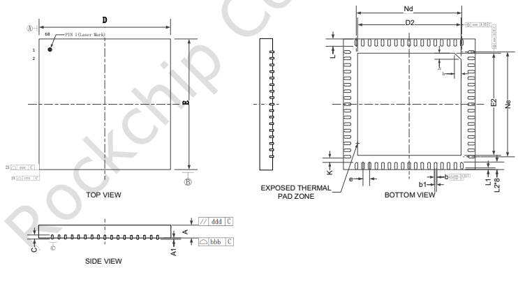
Fig.2-1 QFN68 dimensions — English original, Rev1.3, PDF page 13.
| Symbol |
Minimum / mm |
Nominal / mm |
Maximum / mm |
| A |
0.80 |
0.85 |
0.90 |
| A1 |
- |
0.02 |
0.05 |
| b |
0.10 |
0.15 |
0.20 |
| b1 |
0.08 REF |
|
|
| C |
0.18 |
0.20 |
0.25 |
| D |
6.90 |
7.00 |
7.10 |
| D2 |
5.39 |
5.49 |
5.59 |
| e |
0.35BSC |
|
|
| Nd |
5.60BSC |
|
|
| E |
6.90 |
7.00 |
7.10 |
| E2 |
5.39 |
5.49 |
5.59 |
| Ne |
5.60BSC |
|
|
| L |
0.35 |
0.40 |
0.45 |
| L1 |
0.10BSC |
|
|
| L2 |
0.35 |
0.40 |
0.45 |
| k |
0.20 |
- |
- |
| h |
0.30 |
0.35 |
0.40 |
| aaa |
0.07 |
|
|
| bbb |
0.08 |
|
|
| ccc |
0.10 |
|
|
| ddd |
0.10 |
|
|
| eee |
0.10 |
|
|
| fff |
0.05 |
|
|
Single-value REF/BSC and geometric tolerance cells span the source min/nom/max columns; the value is shown once, not an independent minimum.
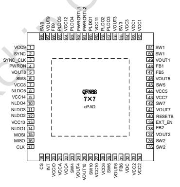
Fig.2-2 Pin assignment, pitch0.35mm — English original, Rev1.3, PDF page 14.
| Pin |
Name |
Description |
I/O |
| 1 |
VCC9 |
Power supply of buck9. |
I |
| 2 |
SYNC |
Master and slave synchronization signal. |
I/O |
| 3 |
SYNC_CLK |
32k synchronization clk. |
I/O |
| 4 |
PWRON |
Power on key. The internal pull-up resistance is about 45K to VCCA. |
I |
| 5 |
VOUT8 |
Output feedback voltage of buck8. |
I |
| 6 |
SW8 |
Switching node of buck8. |
O |
| 7 |
VCC8 |
Power supply of buck8. |
I |
| 8 |
NLDO5 |
NMOS LDO5 output. |
O |
| 9 |
VCC14 |
Power supply of NLDO4/5. |
I |
| 10 |
NLDO4 |
NMOS LDO4 output. |
O |
| 11 |
NLDO3 |
NMOS LDO3 output. |
O |
| 12 |
NLDO2 |
NMOS LDO2 output. |
O |
| 13 |
VCC13 |
Power supply of NLDO1/2/3. |
I |
| 14 |
NLDO1 |
NMOS LDO1 output. |
O |
| 15 |
MOSI/SDA |
SPI MOSI. I2C SDA. |
I/O |
| 16 |
MISO/PWRCRTL3 |
SPI MISO. PWRCRTL3 control. |
I/O |
| 17 |
CLK/SCL |
SPI CLK. I2C SCL. |
I |
| 18 |
CS |
Select SPI/I2C mode when powering on. (I2C mode when connecting to VCCA, SPI mode when not connecting to VCCA). In SPI mode, use for CS pin of SPI |
I |
| 19 |
INT |
Interrupt. |
O |
| 20 |
VCCIO |
Output for I2C/SPI. |
O |
| 21 |
VCCA |
Analog power supply. Power supply of PLDO6/RESETB/INT and system logic. |
I |
| 22 |
VCC4 |
Power supply of buck4. |
I |
| 23 |
SW4 |
Switching node of buck4. |
O |
| 24 |
VOUT4 |
Output feedback voltage of buck4. |
I |
| 25 |
VOUT10 |
Output feedback voltage of buck10. |
I |
| 26 |
SW10 |
Switching node of buck10. |
O |
| 27 |
VCC10 |
Power supply of buck10. |
I |
| 28 |
VCC6 |
Power supply of buck6. |
I |
| 29 |
SW6 |
Switching node of buck6. |
O |
| 30 |
VOUT6 |
Output feedback voltage of buck6. |
I |
| 31 |
FB6 |
Extended divided resistor mode feedback voltage of buck6. |
I |
| 32 |
VDC |
VDC power on signal. |
I |
| 33 |
VCC2 |
Power supply of buck2. |
I |
| 34 |
VCC2 |
Power supply of buck2. |
I |
| 35 |
SW2 |
Switching node of buck2. |
O |
| 36 |
SW2 |
Switching node of buck2. |
O |
| 37 |
VOUT2 |
Output feedback voltage of buck2. |
I |
| 38 |
FB2 |
External divided resistor mode feedback voltage of buck2. |
I |
| 39 |
EXT_EN |
Control extended DCDC enable. Master/Slave select. |
I/O |
| 40 |
RESETB |
Reset the AP. The equivalent capacitance of this foot to GND cannot be greater than 0.3uF |
I/O |
| 41 |
VOUT7 |
Output feedback voltage of buck7. |
I |
| 42 |
SW7 |
Switching node of buck7. |
O |
| 43 |
VCC7 |
Power supply of buck7. |
I |
| 44 |
VCC5 |
Power supply of buck5. |
I |
| 45 |
SW5 |
Switching node of buck5. |
O |
| 46 |
VOUT5 |
Output feedback voltage of buck5. |
I |
| 47 |
FB5 |
External divided resistor mode feedback voltage of buck5. |
I |
| 48 |
FB1 |
External divided resistor mode feedback voltage of buck1. |
I |
| 49 |
VOUT1 |
Output feedback voltage of buck1. |
I |
| 50 |
SW1 |
Switching node of buck1. |
O |
| 51 |
SW1 |
Switching node of buck1. |
O |
| 52 |
VCC1 |
Power supply of buck1. |
I |
| 53 |
VCC1 |
Power supply of buck1. |
I |
| 54 |
VCC3 |
Power supply of buck3. |
I |
| 55 |
SW3 |
Switching node of buck3. |
O |
| 56 |
VOUT3 |
Output feedback voltage of buck3. |
I |
| 57 |
PLDO3 |
PMOS LDO3 output. |
O |
| 58 |
PLDO2 |
PMOS LDO2 output. |
O |
| 59 |
VCC11 |
Power supply of PLDO1/2/3. |
I |
| 60 |
PLDO1 |
PMOS LDO1 output. |
O |
| 61 |
PWRCRTL2 |
PWRCRTL2 control. |
I/O |
| 62 |
PWRCRTL1 |
PWRCRTL1 control. |
I/O |
| 63 |
PLDO4 |
PMOS LDO4 output. |
O |
| 64 |
VCC12 |
Power supply of PLDO4/5. |
I |
| 65 |
PLDO5 |
PMOS LDO5 output. |
O |
| 66 |
FB9 |
External divided resistor mode feedback voltage of buck9. |
I |
| 67 |
VOUT9 |
Output feedback voltage of buck9. |
I |
| 68 |
SW9 |
Switching node of buck9. |
O |
| Exposed |
ePAD |
Ground |
|
3 Electrical characteristics
Exceeding absolute maximum ratings may permanently damage the device and compromise device/system reliability and safety. Functional operation outside recommended conditions is not guaranteed. Unless stated otherwise, typical electrical data use VCCA=5.0V,TA=25°C. VCCA is the analog supply and must be≥VCC1–VCC14. Source spellings EST_EN and SYNS_CLK in the electrical table are preserved, distinct from EXT_EN/SYNC_CLK elsewhere. The NLDO/PLDO accuracy rows often give0.99/1/1.01V while their notes name different nominal voltages; both columns are retained without silently correcting the source.
3.1 Absolute maximum ratings
| Parameter |
Min |
Max |
Unit |
| Voltage range all pins |
-0.3 |
6.5 |
V |
| Voltage range on pins SWx |
-0.3(-2V for <20ns and -3.5V for <10ns) |
6.5(7V for <20ns) |
V |
| Storage temperature range, T S |
-40 |
150 |
℃ |
| Operating temperature range, T J |
-40 |
125 |
℃ |
| Maximum Soldering Temperature, T SOLDER |
|
300 |
℃ |
3.2 Recommended operating conditions
| Parameter |
Min |
Typical |
Max |
Unit |
| Voltage range on pins VCCx/VCCA/SYNC/ SYNC_CLK/VDC/PWRON/EST_EN/CS/RESETB/INT |
2.7 |
5 |
5.5 |
V |
| Power Dissipation |
|
|
2 |
W |
| Voltage range on pin VCCIO/MOSI/MISO/ PWRCRTL1/ PWRCRTL2 |
1.62 |
|
3.4 |
V |
| Parameter |
Symbol |
Condition / note |
Min |
Typical |
Max |
Unit |
| I2C interface (7bits I2C address :Master I2C address is 0x23, Slave I2C address is 0x25) |
|
|
|
|
|
|
| SCL clock frequency |
f SCL |
|
|
|
1000 |
KHz |
| LOGIC INPUT |
|
|
|
|
|
|
| Input LOW-Level Voltage:PWRON,SYNC,SYNS_CLK |
V IL |
|
|
|
0.3+VCCA |
V |
| Input LOW-Level Voltage: VDC |
V IL1 |
|
|
|
0.65 |
V |
| Input HIGH-Level Voltage: MOSI,MISO,CS,PWRCRTL1/2, RESETB,INT |
V IH1 |
|
VCCIO*0.7 |
|
0.3+VCCIO |
V |
| Input HIGH-Level Voltage: PWRON , VCCx,VCCA,SYNC, SYNC_CLK |
V IH2 |
|
VCCA*0.7 |
|
0.3+VCCA |
V |
| Input HIGH-Level Voltage: VDC |
V IH3 |
|
0.88 |
|
|
V |
3.3 DC characteristics
| Parameter |
Symbol |
Condition / note |
Min |
Typical |
Max |
Unit |
| Power dissipation |
|
|
|
|
|
|
| Shut down Current |
Isd |
|
|
10 |
12 |
uA |
| Power on current 1: All bucks, LDOs power on, Null load |
Iq1 |
|
|
1.8 |
|
mA |
| Power on and sleep current: All bucks, LDOs power on, low power mode, sleep mode, Null load |
Isleep |
|
|
0.85 |
|
mA |
| System Characteristics |
|
|
|
|
|
|
| VB_UV threshold, when the VCCx voltage is lower than it, The PMIC would be shutdown. |
Vuv |
2.7V~3.4 V by I2C programmed. Typical is 2.7V. VB_UV_SEL=0b000 |
2.646 |
2.7 |
2.754 |
V |
| |
|
VB_UV_SEL=0b011 |
2.94 |
3.0 |
3.06 |
V |
| |
|
VB_UV_SEL=0b111 |
3.332 |
3.4 |
3.468 |
V |
| VB_LO threshold, when the VCCx voltage is lower than it, The PMIC would be shut down or interrupt happen. |
Vlo |
2.8V~3.5 V by I2C programmed. Typical is 3.2V. VB_LO_SEL= 0b000 |
2.744 |
2.8 |
2.856 |
V |
| |
|
VB_LO_SEL= 0b100 |
3.136 |
3.2 |
3.264 |
V |
| |
|
VB_LO_SEL= 0b111 |
3.43 |
3.5 |
3.57 |
V |
| VB_OV threshold, when the VCCx voltage is higher than it, The PMIC would be shutdown. |
Vov |
|
5.8 |
6.0 |
6.2 |
V |
| TSD threshold, when the temperature is higher than it, The PMIC would be shutdown. |
Tsd |
140/160 ℃ by I2C/SPI programmed. Typical is 160℃. TSD_TEMP=0b0 |
135 |
140 |
145 |
℃ |
| |
|
TSD_TEMP=0b1 |
155 |
160 |
165 |
℃ |
| T warning threshold, when the temperature is higher than it, interrupt happen. |
Twa |
85~115 ℃ by I2C/SPI programmed. Typical is 115℃. HOTDIE_TEMP[ 1:0]=0b00 |
80 |
85 |
90 |
℃ |
| |
|
HOTDIE_TEMP= 0b01 |
90 |
95 |
100 |
℃ |
| |
|
HOTDIE_TEMP= 0b10 |
100 |
105 |
110 |
℃ |
| |
|
HOTDIE_TEMP= 0b11 |
110 |
115 |
120 |
℃ |
| Long press PWRON key time |
Tlp |
6s~12s by I2C/SPI programmed. Typical is 6s. PWRON_LP_OFF_TIME=0b00 |
5.76 |
6 |
6.24 |
s |
| |
|
PWRON_LP_OFF_TIME=0b01 |
7.68 |
8 |
8.32 |
s |
| |
|
PWRON_LP_OFF_TIME=0b10 |
9.6 |
10 |
10.4 |
s |
| |
|
PWRON_LP_OFF_TIME=0b11 |
11.52 |
12 |
12.48 |
s |
| The frequency of RC oscillator is 32.768 kHz |
32KHz clock |
|
31.45 |
32.768 |
34.08 |
kHz |
| Short press PWRON key time |
Tst |
20ms/500ms by I2C/SPI programmed and OTP programmed. Typical is 500ms. PWRON_ON_TIME=0b0 |
480 |
500 |
520 |
ms |
| |
|
PWRON_ON_TIME=0b1 |
19.2 |
20 |
20.8 |
ms |
| Start up sequence |
|
|
|
|
|
|
| 1mS intervals between the channels to start up |
|
|
0.96 |
1 |
1.04 |
mS |
| BUCK1: Fast load transient response step-down converter |
|
|
|
|
|
|
| Input supply voltage range |
Vcc1 |
|
2.7 |
|
5.5 |
V |
| Feedback Voltage, Default |
Vfb1 |
Selection of external resistor divider, R1=R2=100K |
0.99 |
1.0 |
1.01 |
V |
| Internal Feedback Reference |
Vref_exfb |
Default disable. Enable in Register 0xFD<0>=1. |
0.495 |
0.5 |
0.505 |
V |
| Output Voltage Accuracy @ all load @ all input voltage range |
Vfb1 |
If internal divide mode selected: 0.5V~3.4V by I2C/SPI programmed. Typical is 0.8V.Adjust in Register 0x1A, Step=6.25mV. |
0.792 |
0.8 |
0.808 |
V |
| Load Transient Response L=0.22uH, Cout=66uF. |
Vdrop1 |
0.65A to 6.5A, 1A/uS, Vout=0.8V |
|
38 |
|
mV |
| Rated output current |
Imax1 |
|
6.5 |
|
|
A |
| Switching Frequency when CCM mode (Vin=3.8V,Vout=1.5V) |
Fsw1 |
Vin-Vout>1.5V |
1.89 |
2.1 |
2.31 |
MHz |
| Conversion Efficiency (Vin=4.2V,Vout=0.8V) |
|
Iout=6.5A Iout=1.5A Iout=0.65A |
|
68 85 81 |
|
% |
| BUCK2: Fast load transient response step-down converter |
|
|
|
|
|
|
| Input supply voltage range |
Vcc2 |
|
2.7 |
|
5.5 |
V |
| Feedback Voltage, Default |
Vfb2 |
Selection of external resistor divider, R1=R2=100K |
0.99 |
1.0 |
1.01 |
V |
| Internal Feedback Reference |
Vref_exfb |
Default disable. Enable in Register 0xFD<1>=1. |
0.495 |
0.5 |
0.505 |
V |
| Output Voltage Accuracy @ all load @ all input voltage range |
Vfb2 |
If internal divide mode selected: 0.5V~3.4V by I2C /SPI programmed. Typical is 0.8V. Adjust in Register 0x1B, Step=6.25mV. |
0.792 |
0.8 |
0.808 |
V |
| Load Transient Response L=0.22uH, Cout=66uF. |
Vdrop2 |
0.5A to 5A, 1A/uS, Vout=0.8V |
|
30 |
|
mV |
| Rated output current |
Imax2 |
|
5 |
|
|
A |
| Switching Frequency when CCM mode (Vin=3.8V,Vout=1.5V) |
Fsw2 |
Vin-Vout>1.5V |
1.89 |
2.1 |
2.31 |
MHz |
| Conversion Efficiency (Vin=4.2V,Vout=0.8V) |
|
Iout=5A Iout=1A Iout=0.5A |
|
67 84 81 |
|
% |
| BUCK3: Fast load transient response step-down converter |
|
|
|
|
|
|
| Input supply voltage range |
Vcc3 |
|
2.7 |
|
5.5 |
V |
| Output Voltage Accuracy @ all load @ all input voltage range |
Vbuck3 |
0.5V~3.4V by I2C /SPI programmed. Typical is 0.8V. Adjust in Register 0x1C, Step=6.25mV |
0.792 |
0.8 |
0.808 |
V |
| Load Transient Response L=0.22uH, Cout=66uF. |
Vdrop3 |
0.5A to 5.0A, 1A/uS, Vout=0.8V |
|
30 |
|
mV |
| Rated output current |
Imax3 |
|
5 |
|
|
A |
| Switching Frequency when CCM mode (Vin=3.8V,Vout=1.5V) |
Fsw3 |
Vin-Vout>1.5V |
1.89 |
2.1 |
2.31 |
MHz |
| Conversion Efficiency (Vin=4.2V,Vout=0.8V) |
|
Iout=5A Iout=1A Iout=0.5A |
|
66 84 82 |
|
% |
| BUCK4: Fast load transient response step-down converter |
|
|
|
|
|
|
| Input supply voltage range |
Vcc4 |
|
2.7 |
|
5.5 |
V |
| Output Voltage Accuracy @ all load @ all input voltage range |
Vfb4 |
0.5V~3.4V by I2C /SPI programmed. Typical is 0.8V. Adjust in Register 0x1D, Step=6.25mV |
0.792 |
0.8 |
0.808 |
V |
| Load Transient Response L=0.22uH, Cout=66uF. |
Vdrop4 |
0.5A to 5A, 1A/uS, Vout=0.8V |
|
22 |
|
mV |
| Rated output current |
Imax4 |
|
5 |
|
|
A |
| Switching Frequency when CCM mode (Vin=3.8V,Vout=1.5V) |
Fsw4 |
Vin-Vout>1.5V |
1.89 |
2.1 |
2.31 |
MHz |
| Conversion Efficiency (Vin=4.2V,Vout=0.8V) |
|
Iout=5A Iout=1A Iout=0.5A |
|
66 84 82 |
|
% |
| BUCK5: Fast load transient response step-down converter |
|
|
|
|
|
|
| Input supply voltage range |
Vcc5 |
|
2.7 |
|
5.5 |
V |
| Feedback Voltage, Default |
Vfb5 |
Selection of external resistor divider, R1=R2=100K. |
0.99 |
1.0 |
1.01 |
V |
| Internal Feedback Reference |
Vref_exfb |
Default disable. Enable in Register 0xFD<4>=1. |
0.495 |
0.5 |
0.505 |
V |
| Output Voltage Accuracy @ all load @ all input voltage range |
Vfb5 |
If internal divide mode selected: 0.5V~3.4V by I2C /SPI programmed. Typical is 0.8V. Adjust in Register 0x1E, Step=6.25mV. |
0.792 |
0.8 |
0.808 |
V |
| Load Transient Response L=470nH, Cout=44uF. |
Vdrop5 |
0.3A to 3A, 1A/uS, Vout=0.8V |
|
20 |
|
mV |
| Rated output current |
Imax5 |
|
3 |
|
|
A |
| Switching Frequency when CCM mode (Vin=3.8V,Vout=1.5V) |
Fsw5 |
Vin-Vout>1.5V |
1.89 |
2.1 |
2.31 |
MHz |
| Conversion Efficiency (Vin=4.2V,Vout=0.8V) |
|
Iout=3A Iout=1A Iout=0.25A |
|
65 82 81 |
|
% |
| BUCK6: Fast load transient response step-down converter |
|
|
|
|
|
|
| Input supply voltage range |
Vcc6 |
|
2.7 |
|
5.5 |
V |
| Feedback Voltage, Default |
Vfb6 |
Selection of external resistor divider, R1=R2=100K. |
0.99 |
1.0 |
1.01 |
V |
| Internal Feedback Reference |
Vref_exfb |
Default disable. Enable in Register 0xFD<5>=1. |
0.495 |
0.5 |
0.505 |
V |
| Output Voltage Accuracy @ all load @ all input voltage range |
Vfb6 |
If internal divide mode selected: 0.5V~3.4V by I2C/SPI programmed. Typical is 0.8V. Adjust in Register 0x1F, Step=6.25mV. |
0.792 |
0.8 |
0.808 |
V |
| Load Transient Response L=470nH, Cout=44uF. |
Vdrop6 |
0.3A to 3A, 1A/uS, Vout=0.8V |
|
20 |
|
mV |
| Rated output current |
Imax6 |
|
3 |
|
|
A |
| Switching Frequency when CCM mode (Vin=3.8V,Vout=1.5V) |
Fsw6 |
Vin-Vout>1.5V |
1.89 |
2.1 |
2.31 |
MHz |
| Conversion Efficiency (Vin=4.2V,Vout=0.8V) |
|
Iout=2.5A Iout=1A Iout=0.25A |
|
65 82 81 |
|
% |
| BUCK7: Fast load transient response step-down converter |
|
|
|
|
|
|
| Input supply voltage range |
Vcc7 |
|
2.7 |
|
5.5 |
V |
| Output Voltage Accuracy @ all load @ all input voltage range |
Vfb7 |
0.5V~3.4V by I2C /SPI programmed. Typical is 0.8V. Adjust in Register 0x20, Step=6.25mV. |
0.792 |
0.8 |
0.808 |
V |
| Load Transient Response L=470nH, Cout=44uF. |
Vdrop7 |
0.3A to 3A, 1A/uS, Vout=0.8V |
|
22 |
|
mV |
| Rated output current |
Imax7 |
|
3 |
|
|
A |
| Switching Frequency when CCM mode (Vin=3.8V,Vout=1.5V) |
Fsw7 |
Vin-Vout>1.5V |
1.89 |
2.1 |
2.31 |
MHz |
| Conversion Efficiency (Vin=4.2V,Vout=0.8V) |
|
Iout=3A Iout=1A Iout=0.25A |
|
65 82 81 |
|
% |
| BUCK8: Fast load transient response step-down converter |
|
|
|
|
|
|
| Input supply voltage range |
Vcc8 |
|
2.7 |
|
5.5 |
V |
| Output Voltage Accuracy @ all load @ all input voltage range |
Vfb8 |
0.5V~3.4V by I2C / SPI programmed. Typical is 0.8V. Adjust in Register 0x21, Step=6.25mV |
0.792 |
0.8 |
0.808 |
V |
| Load Transient Response L=470nH, Cout=44uF. |
Vdrop8 |
0.3A to 3A, 1A/uS, Vout=0.8V |
|
22 |
|
mV |
| Rated output current |
Imax8 |
|
3 |
|
|
A |
| Switching Frequency when CCM mode (Vin=3.8V,Vout=1.5V) |
Fsw8 |
Vin-Vout>1.5V |
1.89 |
2.1 |
2.31 |
MHz |
| Conversion Efficiency (Vin=4.2V,Vout=0.8V) |
|
Iout=3A Iout=1A Iout=0.25A |
|
65 82 81 |
|
% |
| BUCK9: Fast load transient response step-down converter |
|
|
|
|
|
|
| Input supply voltage range |
Vcc9 |
|
2.7 |
|
5.5 |
V |
| Feedback Voltage, Default |
Vfb9 |
Selection of external resistor divider, R1=R2=100K. |
0.99 |
1.0 |
1.01 |
V |
| Internal Feedback Reference |
Vref_exfb |
Default disable. Enable in Register 0xFE<0>=1. |
0.495 |
0.5 |
0.505 |
V |
| Output Voltage Accuracy @ all load @ all input voltage range |
Vfb9 |
If internal divide mode selected: 0.5V~3.4V by I2C / SPI programmed. Typical is 0.8V. Adjust in Register 0x22, Step=6.25mV |
0.784 |
0.8 |
0.816 |
V |
| Load Transient Response L=470nH, Cout=44uF. |
Vdrop9 |
0.3A to 3A, 1A/uS, Vout=0.8V |
|
20 |
|
mV |
| Rated output current |
Imax9 |
|
3 |
|
|
A |
| Switching Frequency when CCM mode (Vin=3.8V,Vout=1.5V) |
Fsw9 |
Vin-Vout>1.5V |
1.89 |
2.1 |
2.31 |
MHz |
| Conversion Efficiency (Vin=4.2V,Vout=0.8V) |
|
Iout=3A Iout=1A Iout=0.25A |
|
65 82 81 |
|
% |
| BUCK10: Fast load transient response step-down converter |
|
|
|
|
|
|
| Input supply voltage range |
Vcc10 |
|
2.7 |
|
5.5 |
V |
| Output Voltage Accuracy @ all load @ all input voltage range |
Vfb10 |
0.5V~3.4V by I2C / SPI programmed. Typical is 0.8V. Adjust in Register 0x23, Step=6.25mV |
0.792 |
0.8 |
0.808 |
V |
| Load Transient Response L=470nH, Cout=44uF. |
Vdrop10 |
0.3A to 3A, 0.5A/uS, Vout=0.8V |
|
22 |
|
mV |
| Rated output current |
Imax10 |
|
3 |
|
|
A |
| Switching Frequency when CCM mode (Vin=3.8V,Vout=1.5V) |
Fsw10 |
Vin-Vout>1.5V |
1.89 |
2.1 |
2.31 |
MHz |
| Conversion Efficiency (Vin=4.2V,Vout=0.8V) |
|
Iout=3A Iout=1A Iout=0.25A |
|
65 82 81 |
|
% |
| NLDO1 |
|
|
|
|
|
|
| Input supply voltage range |
Vcc13 |
VCCA-NLDO1>1.5V |
0.6 |
|
5.5 |
V |
| Output Voltage Accuracy @ all load @ all input voltage range |
Vnldo1 |
0.5V~3.4V by I2C / SPI programmed. Typical is 1V. Adjust in Register 0x43, Step=12.5mV . |
0.99 |
1 |
1.01 |
V |
| Rated output current |
Imaxl1 |
Vcc13-Vnldo1>0.2V |
300 |
|
|
mA |
| PSRR@ 1KHz |
|
Vin rms=200mV |
|
65 |
|
dB |
| PSRR@ 10KHz |
|
Vin rms=200mV |
|
60 |
|
dB |
| NLDO2 |
|
|
|
|
|
|
| Input supply voltage range |
Vcc13 |
VCCA-NLDO2>1.5V |
0.6 |
|
5.5 |
V |
| Output Voltage Accuracy @ all load @ all input voltage range |
Vnldo2 |
0.5V~3.4V by I2C SPI programmed. Typical is 1.8V. Adjust in Register 0x44, Step=12.5mV |
0.99 |
1 |
1.01 |
V |
| Rated output current |
Imaxl2 |
Vcc13-Vnldo2>0.2V |
300 |
|
|
mA |
| PSRR@ 1KHz |
|
Vin rms=200mV |
|
65 |
|
dB |
| PSRR@ 10KHz |
|
Vin rms=200mV |
|
60 |
|
dB |
| NLDO3 |
|
|
|
|
|
|
| Input supply voltage range |
Vcc13 |
VCCA-NLDO3>1.5V |
0.6 |
|
5.5 |
V |
| Output Voltage Accuracy @ all load @ all input voltage range |
Vnldo3 |
0.5V~3.4V by I2C /SPI programmed. Typical is 1V. Adjust in Register 0x45, Step=12.5mV |
0.99 |
1 |
1.01 |
V |
| Rated output current |
Imaxl3 |
Vcc13-Vnldo3>0.2V |
500 |
|
|
mA |
| PSRR@ 1KHz |
|
Vin rms=200mV |
|
65 |
|
dB |
| PSRR@ 10KHz |
|
Vin rms=200mV |
|
60 |
|
dB |
| NLDO4 |
|
|
|
|
|
|
| Input supply voltage range |
Vcc14 |
VCCA-NLDO4>1.5V |
0.6 |
|
5.5 |
V |
| Output Voltage Accuracy @ all load @ all input voltage range |
Vnldo4 |
0.5V~3.4V by I2C /SPI programmed. Typical is 1V. Adjust in Register 0x46, Step=12.5mV |
0.99 |
1 |
1.01 |
V |
| Rated output current |
Imaxl4 |
Vcc14-Vnldo4>0.2V |
500 |
|
|
mA |
| PSRR@ 1KHz |
|
Vin rms=200mV |
|
65 |
|
dB |
| PSRR@ 10KHz |
|
Vin rms=200mV |
|
60 |
|
dB |
| NLDO5 |
|
|
|
|
|
|
| Input supply voltage range |
Vcc14 |
VCCA-NLDO5>1.5V |
0.6 |
|
5.5 |
V |
| Output Voltage Accuracy @ all load @ all input voltage range |
Vnldo5 |
0.5V~3.4V by I2C /SPI programmed. Typical is 3V. Adjust in Register 0x47, Step=12.5mV |
0.99 |
1 |
1.01 |
V |
| Rated output current |
Imaxl5 |
Vcc14-Vnldo5>0.2V |
300 |
|
|
mA |
| PSRR@ 1KHz |
|
Vin rms=200mV |
|
65 |
|
dB |
| PSRR@ 10KHz |
|
Vin rms=200mV |
|
60 |
|
dB |
| PLDO1 |
|
|
|
|
|
|
| Input supply voltage range |
Vcc11 |
|
1.9 |
|
5.5 |
V |
| Output Voltage Accuracy @ all load @ all input voltage range |
Vpldo1 |
0.5V~3.4V by I2C /SPI programmed. Typical is 3V. Adjust in Register 0x4E, Step=12.5mV |
0.99 |
1 |
1.01 |
V |
| Rated output current |
Imaxl1 |
Vcc11-Vpldo1>0.2V VCC11≥2.0V |
500 |
|
|
mA |
| |
|
Vcc11-Vpldo1>0.1V |
250 |
|
|
mA |
| PSRR@ 1KHz |
|
Vin rms=200mV |
|
65 |
|
dB |
| PSRR@ 10KHz |
|
Vin rms=200mV |
|
60 |
|
dB |
| PLDO2 |
|
|
|
|
|
|
| Input supply voltage range |
Vcc11 |
|
1.9 |
|
5.5 |
V |
| Output Voltage Accuracy @ all load @ all input voltage range |
Vpldo2 |
0.5V~3.4V by I2C /SPI programmed. Typical is 2.8V. Adjust in Register 0x4F, Step=12.5mV |
0.99 |
1 |
1.01 |
V |
| Rated output current |
Imaxl2 |
Vcc11-Vpldo2>0.2V, VCC11≥2.0V |
300 |
|
|
mA |
| |
|
Vcc11-Vpldo2>0.1V |
150 |
|
|
mA |
| PSRR@ 1KHz |
|
Vin rms=200mV |
|
65 |
|
dB |
| PSRR@ 10KHz |
|
Vin rms=200mV |
|
60 |
|
dB |
| PLDO3 |
|
|
|
|
|
|
| Input supply voltage range |
Vcc11 |
|
1.9 |
|
5.5 |
V |
| Output Voltage Accuracy @ all load @ all input voltage range |
Vpldo3 |
0.5V~3.4V by I2C /SPI programmed. Typical is 1.8V. Adjust in Register 0x50, Step=12.5mV |
0.99 |
1 |
1.01 |
V |
| Rated output current |
Imaxl3 |
Vcc11-Vpldo3>0.2V, VCC11≥2.0V |
300 |
|
|
mA |
| |
|
Vcc11-Vpldo3>0.1V |
150 |
|
|
mA |
| PSRR@ 1KHz |
|
Vin rms=200mV |
|
65 |
|
dB |
| PSRR@ 10KHz |
|
Vin rms=200mV |
|
60 |
|
dB |
| PLDO4 |
|
|
|
|
|
|
| Input supply voltage range |
Vcc12 |
|
1.9 |
|
5.5 |
V |
| Output Voltage Accuracy @ all load @ all input voltage range |
Vpldo4 |
0.5V~3.4V by I2C /SPI programmed. Typical is 1.5V. Adjust in Register 0x51, Step=12.5mV |
0.99 |
1 |
1.01 |
V |
| Rated output current |
Imaxl4 |
Vcc12-Vpldo4>0.2V, Vcc12>2.0 |
500 |
|
|
mA |
| |
|
Vcc12-Vpldo4>0.1V |
250 |
|
|
mA |
| PSRR@ 1KHz |
|
Vin rms=200mV |
|
65 |
|
dB |
| PSRR@ 10KHz |
|
Vin rms=200mV |
|
60 |
|
dB |
| PLDO5 |
|
|
|
|
|
|
| Input supply voltage range |
Vcc12 |
|
1.9 |
|
5.5 |
V |
| Output Voltage Accuracy @ all load @ all input voltage range |
Vpldo5 |
0.5V~3.4V by I2C /SPI programmed. Typical is 1.8V. Adjust in Register 0x52, Step=12.5mV |
0.99 |
1 |
1.01 |
V |
| Rated output current |
Imaxl5 |
Vcc12-Vpldo5>0.2V VCC12≥2.0V |
300 |
|
|
mA |
| |
|
Vcc12-Vpldo5>0.1V |
150 |
|
|
mA |
| PSRR@ 1KHz |
|
Vin rms=200mV |
|
65 |
|
dB |
| PSRR@ 10KHz |
|
Vin rms=200mV |
|
60 |
|
dB |
| VCCIO |
|
|
|
|
|
|
| Input supply voltage range[1] |
VccA |
|
2.0 |
|
5.5 |
V |
| Output Voltage Accuracy @ all load @ all input voltage range |
Vccio |
0.5V~3.4V by I2C /SPI programmed. Typical is 1.8V. Adjust in Register 0x53, Step=12.5mV |
1.782 |
1.8 |
1.818 |
V |
| Rated output current |
Imaxl6 |
VccA-Vccio>0.2V |
300 |
|
|
mA |
| PSRR@ 1KHz |
|
Vin rms=200mV |
|
65 |
|
dB |
| PSRR@ 10KHz |
|
Vin rms=200mV |
|
60 |
|
dB |
4.1.1–4.1.2 State machine and power-on
The state machine has OFF, ACTIVE and SLEEP states, with power-on/down, reset and sleep-entry/exit transitions. Three power-on methods: (1) With VCCA,VCC1,VCC2 above VB_OK, hold PWRON low for500/20ms, programmable over I2C/SPI. Channels start at default voltages in the preset sequence with1ms intervals. RESETB becomes high after all rails are stable. T1 checks the external supply;3.5ms<T1<100ms is shown, and requirements must be met within100ms. The diagram also shows10ms and≤16ms intervals. (2) With those supplies above VB_OK, VDC high for more than2ms powers on; the same T1 requirement applies. (3) With0x5F<7>=0, OVP/UVLO triggers automatic restart after a powered-on fault; startup completes after normal system voltage is detected.
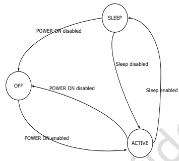
Fig.4-1 State/power-on timing — English original, Rev1.3, PDF page 25.
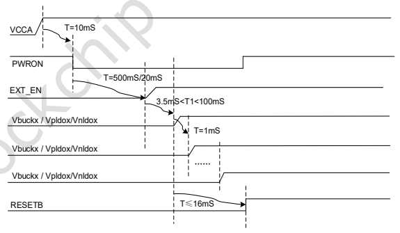
Fig.4-2 State/power-on timing — English original, Rev1.3, PDF page 25.
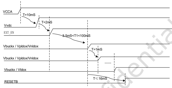
Fig.4-3 State/power-on timing — English original, Rev1.3, PDF page 26.
4.1.3 Power-down
Seven shutdown methods in ON or SLEEP: (1)0x76<6>=0 and PWRON low for6/8/10/12s (I2C-programmable debounce). RESETB goes low, then after1ms channels shut down in the configured sequence; the figure shows1ms spacing and6ms before EXT_EN. (2)Write0x72<0>=1, same sequence. (3)With0x5F<7>=1, any VCCA/VCC1/VCC2 below VB_UV (typ.2.7V) or above VB_OV (typ.6.0V) pulls SYNC low and immediately switches off. (4)With0x5E<3>=0, any of those supplies below VB_LO (typ.3.2V) for1ms shuts down with method1 sequence. (5)PWRCTRLn_FUN=010 and active PWRCTRLn (programmable polarity), same sequence. (6)Temperature above TSD (typ.140°C), same sequence. (7)With0x5F<7>=0, any monitored supply below VB_UV or above VB_OV switches off immediately; the source also says method1 sequence, and both descriptions are retained.
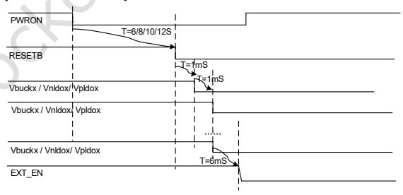
Fig.4-4 PWRON shutdown timing — English original, Rev1.3, PDF page 26.
4.1.4 Reset
The source says four reset methods but lists five.0x72<7:6>=00 means PMIC restart;01 means register reset, restoring all channels to defaults. In ON/SLEEP: (1)0x76<6>=1 and PWRON low6/8/10/12s restarts; debounce is I2C/SPI configurable. The waveform shows1ms channel intervals and244ms. (2)PWRCTRLn_FUN=011 and active PWRCTRLn, polarity set by PWRCTRLn_POL, restarts with the same sequence. (3)Pulling RESETB low restarts immediately, same sequence. (4)WDT active with0x73<4:3>=11 restarts, same sequence. (5)Writing0x72<7:5>=001 restarts, same sequence.
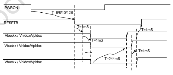
Fig.4-5 PWRON restart timing — English original, Rev1.3, PDF page 27.
4.1.5–4.1.6 Power sequences and sleep
The following power-sequence tables distinguish RK806-1 master, RK806-2 master/slave and RK806-3 master. Short PWRON press is20ms. Notes[1][2][3]: OTP can change default voltages anywhere in0.5–3.4V and startup order. BUCK1/2/5/6/9 can use external feedback resistors for customized values. After power-on, registers B2–C3 set shutdown order. For SLEEP, set PWRCTRLn_FUN=001 and activate PWRCTRLn according to PWRCTRLn_POL. Sleep reduces dissipation;0x0D=FF,0x0C=FF and0x61<1>=1 further reduce quiescent current.
RK806-1(master)
| Channel |
Output range |
Maximum current |
Default voltage |
Startup sequence |
| BUCK1 |
0.5V-3.4V |
6.5A |
0.75V |
5 |
| BUCK2 |
0.5V-3.4V |
5A |
0.75V |
3 |
| BUCK3 |
0.5V-3.4V |
5A |
0.75V |
2 |
| BUCK4 |
0.5V-3.4V |
5A |
0.75V |
5 |
| BUCK5 |
0.5V-3.4V |
3A |
0.85V |
2 |
| BUCK6 |
X(external divided resistor) Or 0.5V-3.4v(internal divided resistor) |
3A |
0.5V |
4 |
| BUCK7 |
0.5V-3.4V |
3A |
2.0V |
1 |
| BUCK8 |
0.5V-3.4V |
3A |
3.3V |
6 |
| BUCK9 |
X(external divided resistor) Or 0.5V-3.4v(internal divided resistor) |
3A |
0.5V |
6 |
| BUCK10 |
0.5V-3.4V |
3A |
1.8V |
3 |
| NLDO1 |
0.5V-3.4V |
300mA |
0.75V |
2 |
| NLDO2 |
0.5V-3.4V |
300mA |
0.85V |
2 |
| NLDO3 |
0.5V-3.4V |
500mA |
0.75V |
2 |
| NLDO4 |
0.5V-3.4V |
500mA |
0.85V |
2 |
| NLDO5 |
0.5V-3.4V |
300mA |
0.75V |
2 |
| PLDO1 |
0.5V-3.4V |
500mA |
1.8V |
3 |
| PLDO2 |
0.5V-3.4V |
300mA |
1.8V |
3 |
| PLDO3 |
0.5V-3.4V |
300mA |
1.2V |
4 |
| PLDO4 |
0.5V-3.4V |
500mA |
3.3V |
6 |
| PLDO5 |
0.5V-3.4V |
300mA |
3.3V |
6 |
| PLDO6 |
0.5V-3.4V |
300mA |
1.8V |
3 |
| VB_OK |
2.8V-3.6V |
x |
2.8V |
x |
| RESETB |
x |
x |
x |
11 |
RK806-2(master)
| Channel |
Output range |
Maximum current |
Default voltage |
Startup sequence |
| BUCK1 |
0.5V-3.4V |
6.5A |
0.75V |
7 |
| BUCK2 |
0.5V-3.4V |
5A |
0.75V |
7 |
| BUCK3 |
0.5V-3.4V |
5A |
0.75V |
2 |
| BUCK4 |
0.5V-3.4V |
5A |
0.75V |
7 |
| BUCK5 |
0.5V-3.4V |
3A |
0.75V |
7 |
| BUCK6 |
0.5V-3.4V |
3A |
0.75V |
7 |
| BUCK7 |
0.5V-3.4V |
3A |
2.0V |
1 |
| BUCK8 |
0.5V-3.4V |
3A |
0.75V |
7 |
| BUCK9 |
X(external divided resistor) Or 0.5V-3.4v(internal divided resistor) |
3A |
0.5V |
4 |
| BUCK10 |
0.5V-3.4V |
3A |
1.10V |
1 |
| NLDO1 |
0.5V-3.4V |
300mA |
0.75V |
2 |
| NLDO2 |
0.5V-3.4V |
300mA |
0.90V |
5 |
| NLDO3 |
0.5V-3.4V |
500mA |
0.75V |
2 |
| NLDO4 |
0.5V-3.4V |
500mA |
0.75V |
2 |
| NLDO5 |
0.5V-3.4V |
300mA |
0.85V |
2 |
| PLDO1 |
0.5V-3.4V |
500mA |
1.80V |
3 |
| PLDO2 |
0.5V-3.4V |
300mA |
1.80V |
3 |
| PLDO3 |
0.5V-3.4V |
300mA |
1.80V |
3 |
| PLDO4 |
0.5V-3.4V |
500mA |
3.30V |
6 |
| PLDO5 |
0.5V-3.4V |
300mA |
3.30V |
6 |
| PLDO6 |
0.5V-3.4V |
300mA |
1.80V |
3 |
| VB_OK |
2.8V-3.6V |
x |
2.8V |
x |
| RESETB |
x |
x |
x |
20 |
RK806-2(slave)
| Channel |
Output range |
Maximum current |
Default voltage |
Startup sequence |
| BUCK1 |
0.5V-3.4V |
6.5A |
0.75V |
9 |
| BUCK2 |
0.5V-3.4V |
5A |
0.75V |
9 |
| BUCK3 |
0.5V-3.4V |
5A |
0.75V |
8 |
| BUCK4 |
0.5V-3.4V |
5A |
3.30V |
6 |
| BUCK5 |
0.5V-3.4V |
3A |
0.75V |
9 |
| BUCK6 |
0.5V-3.4V |
3A |
0.75V |
9 |
| BUCK7 |
0.5V-3.4V |
3A |
1.80V |
3 |
| BUCK8 |
0.5V-3.4V |
3A |
0.75V |
8 |
| BUCK9 |
X(external divided resistor) Or 0.5V-3.4v(internal divided resistor) |
3A |
0.5V |
6 |
| BUCK10 |
0.5V-3.4V |
3A |
0.85V |
2 |
| NLDO1 |
0.5V-3.4V |
300mA |
0.75V |
2 |
| NLDO2 |
0.5V-3.4V |
300mA |
0.85V |
2 |
| NLDO3 |
0.5V-3.4V |
500mA |
0.85V |
2 |
| NLDO4 |
0.5V-3.4V |
500mA |
0.50V |
OFF |
| NLDO5 |
0.5V-3.4V |
300mA |
1.20V |
4 |
| PLDO1 |
0.5V-3.4V |
500mA |
0.50V |
OFF |
| PLDO2 |
0.5V-3.4V |
300mA |
1.80V |
3 |
| PLDO3 |
0.5V-3.4V |
300mA |
1.80V |
3 |
| PLDO4 |
0.5V-3.4V |
500mA |
3.30V |
6 |
| PLDO5 |
0.5V-3.4V |
300mA |
2.80V |
OFF |
| PLDO6 |
0.5V-3.4V |
300mA |
1.80V |
3 |
| VB_OK |
2.8V-3.6V |
x |
2.8V |
x |
| RESETB |
x |
x |
x |
20 |
RK806-3(master)
| Channel |
Output range |
Maximum current |
Default voltage |
Startup sequence |
| BUCK1 |
X(external divided resistor) Or 0.5V-3.4v(internal divided resistor) |
6.5A |
X |
40 |
| BUCK2 |
X(external divided resistor) Or 0.5V-3.4v(internal divided resistor) |
5A |
X |
40 |
| BUCK3 |
0.5V-3.4V |
5A |
0.8V |
0 |
| BUCK4 |
0.5V-3.4V |
5A |
0.8V |
5 |
| BUCK5 |
0.5V-3.4V |
3A |
0.8V |
40 |
| BUCK6 |
0.5V-3.4V |
3A |
0.8V |
45 |
| BUCK7 |
0.5V-3.4V |
3A |
2.0V |
5 |
| BUCK8 |
0.5V-3.4V |
3A |
1.0V |
5 |
| BUCK9 |
0.5V-3.4V |
3A |
1.8V |
45 |
| BUCK10 |
0.5V-3.4V |
3A |
1.8V |
10 |
| NLDO1 |
0.5V-3.4V |
300mA |
0.8V |
40 |
| NLDO2 |
0.5V-3.4V |
300mA |
0.8V |
15 |
| NLDO3 |
0.5V-3.4V |
500mA |
0.8V |
25 |
| NLDO4 |
0.5V-3.4V |
500mA |
1.8V |
20 |
| NLDO5 |
0.5V-3.4V |
300mA |
1.8V |
43 |
| PLDO1 |
0.5V-3.4V |
500mA |
1.8V |
30 |
| PLDO2 |
0.5V-3.4V |
300mA |
1.8V |
35 |
| PLDO3 |
0.5V-3.4V |
300mA |
1.8V |
35 |
| PLDO4 |
0.5V-3.4V |
500mA |
1.8V |
43 |
| PLDO5 |
0.5V-3.4V |
300mA |
1.8V |
55 |
| PLDO6 |
0.5V-3.4V |
300mA |
3.3V |
55 |
| VB_OK |
2.8V-3.6V |
x |
2.8V |
x |
| RESETB |
x |
x |
x |
63 |
4.1.7 Master/slave cooperation
Two RK806 devices may cooperate as master/slave. At first power-on, EXT_EN tied to VCCA selects slave; floating or resistor-pulled-low selects master. Connect both SYNC_CLK pins and both SYNC pins. Master supplies the slave clock on SYNC_CLK; SYNC pulses synchronize startup, shutdown, reset and power transitions. Connect the PWRON pair and RESETB pair respectively for power-on and external-button reset. VDC pins may be joined, or connect slave VDC to master EXT_EN. If host IOs are insufficient, INT pins can also be joined; software reads the respective register sets to distinguish interrupt sources.
4.1.8 I2C and SPI
Master/slave bus addresses are0x23/0x25 (the source calls them register addresses). At first power-on, CS tied to VCCA selects I2C; otherwise SPI. VCCIO must exceed1.62V and must not be disabled in standby. SPI defaults to3-wire. To use4-wire, host initialization sets E8<2>=1; the slave SO pin must be configured with E9<5>=1. Data is prepared on CLK falling edge and latched while CLK is high. Maximum clock20MHz. MISO can serve SLEEP3 only in3-wire mode; join the host MOSI/MISO, exchanging data through PMIC MOSI. After sending SPI data, send two additional dummy bytes. Detailed CRC waveform rules below separately specify the dummy packet count.
| Signal |
Symbol |
Parameter |
Min |
Typical |
Max |
Unit |
| CLK |
Fsclk |
Clock frequency |
— |
— |
20 |
MHz |
| CLK |
th_sclk |
Clock high time |
5 |
25 |
— |
ns |
| CLK |
tl_sclk |
Clock low time |
5 |
25 |
— |
ns |
| CS |
tsu_cs |
CS input setup |
10 |
— |
— |
ns |
| CS |
thold_cs |
CS input hold |
20 |
— |
— |
ns |
| MOSI |
tsu_mosi |
Data input setup |
2 |
— |
— |
ns |
| MOSI |
thold_mosi |
Data input hold |
2 |
— |
— |
ns |
| MISO |
tod_miso |
Clock low to output valid |
— |
20 |
23 |
ns |
Every transfer begins with CMD, REG_L and REG_H. CMD contains R/W[7] (0 read,1 write), CRC_EN[6] (1 enabled,0 disabled), Len[3:0]. With CRC, Len=n−1, maximum16 data bytes; the host/slave sends CRC at position Len+1. Without CRC, Len is ignored and slave register addresses increment within0–255. REG_L is address bits7:0; REG_H is bits15:8 but RK806 ignores it as0. During REG_H in3-wire reads the host switches MO to input to prevent contention as slave SI becomes SO; both sides are inputs and the slave forces received data to0. CRC polynomial is X⁸+X⁴+X+1, initial0x00. The first explanation states REG_L=REG_H=0 during CRC computation; the later definition includes REG_L, REG_H and data. These source statements are retained, not silently reconciled. CRC writes require an additional CRC_CLK_DATA dummy byte after CRC for internal computation/transport; further unrecognized clocks after those8 bits cause CRC_ERR and RK806 stops working. CRC reads require no such dummy byte; clocks beyond CRC produce no response or invalid data. Waveforms: non-CRC single write increments the address after8 clocks regardless of Len; single CRC write adds Dummy1; multibyte CRC write sends at least one dummy packet for≤8 bytes and two for>8 bytes. Four-wire CRC reads return data and CRC on MISO. Three-wire CRC reads include the empty REG_H interval with forced0. Non-CRC reads auto-increment the address every8 clocks. These detailed packet counts coexist with the two-dummy-byte statement in4.1.8.

SPI waveform: spi-command — English original, Rev1.3, PDF page 33.

SPI waveform: spi-write-no-crc — English original, Rev1.3, PDF page 34.

SPI waveform: spi-write-crc — English original, Rev1.3, PDF page 34.

SPI waveform: spi-write-multi-crc — English original, Rev1.3, PDF page 34.

SPI waveform: spi-read-four-wire — English original, Rev1.3, PDF page 34.

SPI waveform: spi-read-three-wire — English original, Rev1.3, PDF page 35.

SPI waveform: spi-read-no-crc — English original, Rev1.3, PDF page 35.
4.2.1 Buck converters
Ten synchronous buck converters deliver up to6.5A,5A or3A. Enhanced constant-on-time (COT) control improves transient response;2MHz switching and the control architecture reduce external inductance/capacitance requirements. DVS permits linear, gradual voltage ramps during operation. Protection includes short-circuit protection. The source example uses BUCK1 at Vout=0.8V,Vin=5V,L=0.22uH,Cout=66uF,load0.065→6.5A,slew3A/uS using a MOSFET transition; rising-load droop is about38mV. Other bucks share the architecture. The electrical table separately specifies0.65→6.5A and1A/uS; these are different source conditions, not ArmSoM test results. The following original figures preserve rising/falling transients and efficiency curves with their plotted conditions.
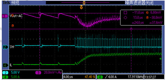
Fig.4-6 BUCK1 load transient — English original, Rev1.3, PDF page 35.
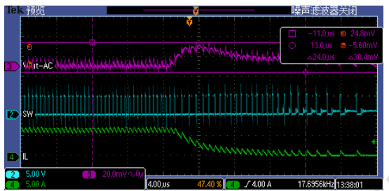
Fig.4-7 BUCK1 load transient — English original, Rev1.3, PDF page 36.
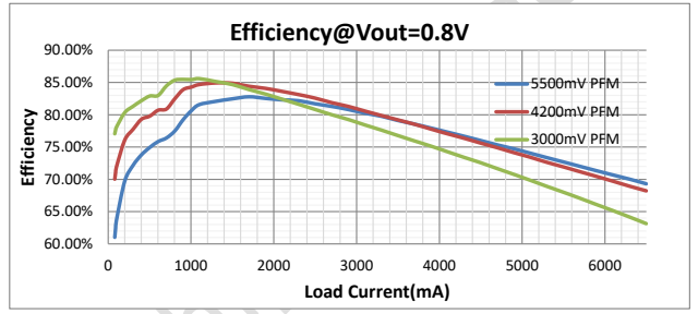
Fig.4-8 BUCK1 efficiency — English original, Rev1.3, PDF page 36.
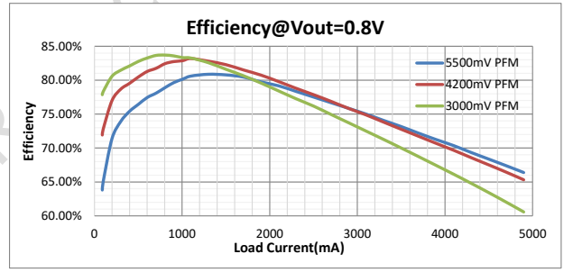
Fig.4-9 BUCK2 efficiency — English original, Rev1.3, PDF page 36.
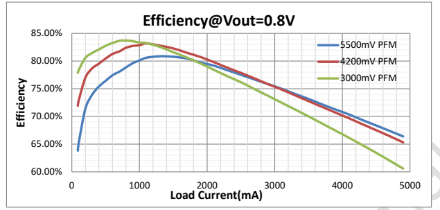
Fig.4-10 BUCK3 efficiency — English original, Rev1.3, PDF page 37.
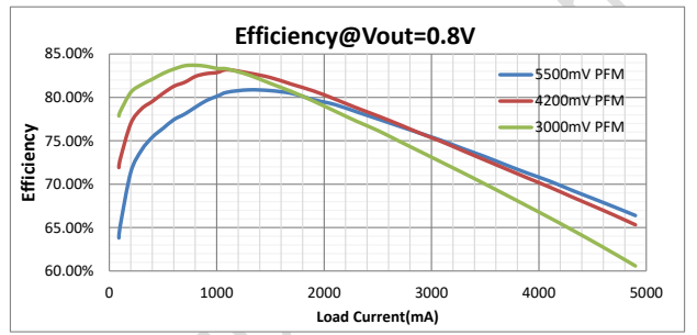
Fig.4-11 BUCK4 efficiency — English original, Rev1.3, PDF page 37.
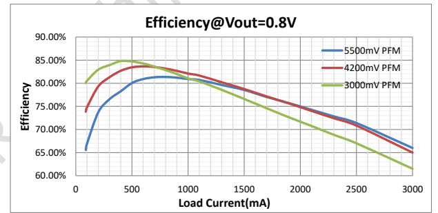
Fig.4-12 BUCK5 efficiency — English original, Rev1.3, PDF page 37.
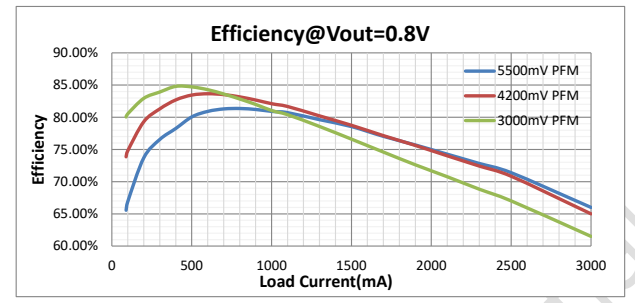
Fig.4-13 BUCK6 efficiency — English original, Rev1.3, PDF page 38.
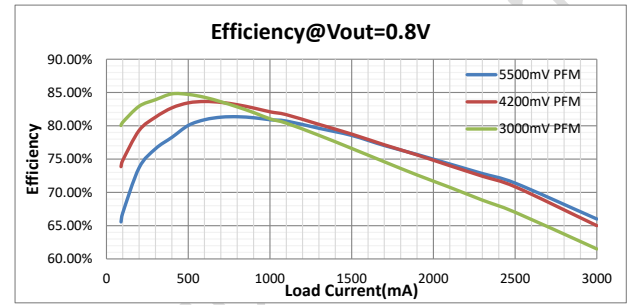
Fig.4-14 BUCK7 efficiency — English original, Rev1.3, PDF page 38.
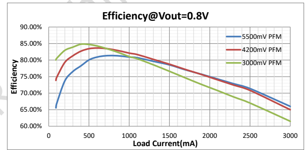
Fig.4-15 BUCK8 efficiency — English original, Rev1.3, PDF page 38.
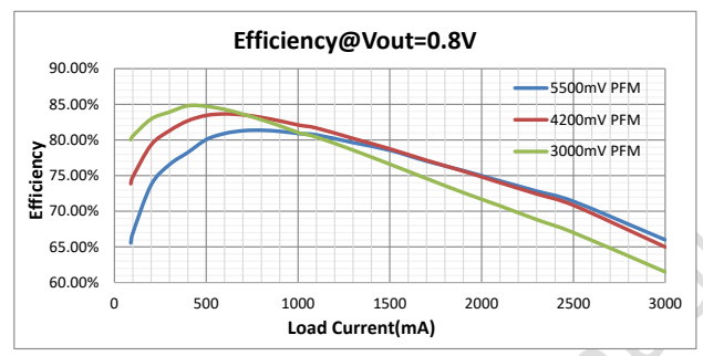
Fig.4-16 BUCK9 efficiency — English original, Rev1.3, PDF page 39.
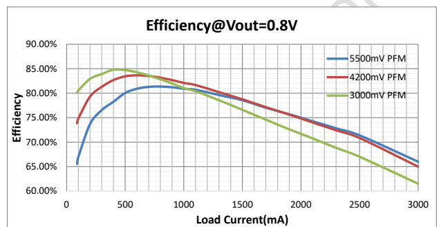
Fig.4-17 BUCK10 efficiency — English original, Rev1.3, PDF page 39.
4.2.2 LDOs
The efficiency test curves use default buck output voltages (plots state0.8V), comparing5500/4200/3000mV input in PFM mode. RK806 integrates five NLDOs: NLDO3/4 up to500mA, NLDO1/2/5 up to300mA; six PLDOs include PLDO1/4 up to500mA. This paragraph lists PLDO2/3/VCCIO at300mA but omits PLDO5; the feature and electrical tables also specify PLDO5 at300mA. All LDO channels may use1.0uF output capacitance to reduce cost. Output voltage and other parameters for different modes are adjustable through I2C/SPI.
5.1 Register summary
| Name |
Offset |
Size |
Reset value |
Description |
| POWER_EN0 |
0x0000 |
B |
OTP |
|
| POWER_EN1 |
0x0001 |
B |
OTP |
|
| POWER_EN2 |
0x0002 |
B |
OTP |
|
| POWER_EN3 |
0x0003 |
B |
OTP |
|
| POWER_EN4 |
0x0004 |
B |
OTP |
|
| POWER_EN5 |
0x0005 |
B |
OTP |
|
| POWER_SLP_EN0 |
0x0006 |
B |
OTP |
|
| POWER_SLP_EN1 |
0x0007 |
B |
OTP |
|
| POWER_SLP_EN2 |
0x0008 |
B |
OTP |
|
| POWER_DISCHRG_EN0 |
0x0009 |
B |
0xff |
|
| POWER_DISCHRG_EN1 |
0x000a |
B |
0xdf |
|
| POWER_DISCHRG_EN2 |
0x000b |
B |
0x3f |
|
| BUCK_FB_CONFIG |
0x000c |
B |
0x01 |
|
| SLP_LP_CONFIG |
0x000d |
B |
0x00 |
|
| POWER_FPWM_EN0 |
0x000e |
B |
0x00 |
|
| POWER_FPWM_EN1 |
0x000f |
B |
0x00 |
|
| BUCK1_CONFIG |
0x0010 |
B |
0x64 |
|
| BUCK2_CONFIG |
0x0011 |
B |
0x64 |
|
| BUCK3_CONFIG |
0x0012 |
B |
0x64 |
|
| BUCK4_CONFIG |
0x0013 |
B |
0x64 |
|
| BUCK5_CONFIG |
0x0014 |
B |
0x64 |
|
| BUCK6_CONFIG |
0x0015 |
B |
0x64 |
|
| BUCK7_CONFIG |
0x0016 |
B |
0x64 |
|
| BUCK8_CONFIG |
0x0017 |
B |
0x64 |
|
| BUCK9_CONFIG |
0x0018 |
B |
0x64 |
|
| BUCK10_CONFIG |
0x0019 |
B |
0x64 |
|
| BUCK1_ON_VSEL |
0x001a |
B |
OTP |
|
| BUCK2_ON_VSEL |
0x001b |
B |
OTP |
|
| BUCK3_ON_VSEL |
0x001c |
B |
OTP |
|
| BUCK4_ON_VSEL |
0x001d |
B |
OTP |
|
| BUCK5_ON_VSEL |
0x001e |
B |
OTP |
|
| BUCK6_ON_VSEL |
0x001f |
B |
OTP |
|
| BUCK7_ON_VSEL |
0x0020 |
B |
OTP |
|
| BUCK8_ON_VSEL |
0x0021 |
B |
OTP |
|
| BUCK9_ON_VSEL |
0x0022 |
B |
OTP |
|
| BUCK10_ON_VSEL |
0x0023 |
B |
OTP |
|
| BUCK1_SLP_VSEL |
0x0024 |
B |
OTP |
|
| BUCK2_SLP_VSEL |
0x0025 |
B |
OTP |
|
| BUCK3_SLP_VSEL |
0x0026 |
B |
OTP |
|
| BUCK4_SLP_VSEL |
0x0027 |
B |
OTP |
|
| BUCK5_SLP_VSEL |
0x0028 |
B |
OTP |
|
| BUCK6_SLP_VSEL |
0x0029 |
B |
OTP |
|
| BUCK7_SLP_VSEL |
0x002a |
B |
OTP |
|
| BUCK8_SLP_VSEL |
0x002b |
B |
OTP |
|
| BUCK9_SLP_VSEL |
0x002c |
B |
OTP |
|
| BUCK10_SLP_VSEL |
0x002d |
B |
OTP |
|
| BUCK_DEBUG13 |
0x003c |
B |
0x44 |
|
| BUCK_DEBUG14 |
0x003d |
B |
0x44 |
|
| BUCK_DEBUG15 |
0x003e |
B |
0x44 |
|
| BUCK_DEBUG16 |
0x003f |
B |
0x44 |
|
| BUCK_DEBUG17 |
0x0040 |
B |
0x44 |
|
| NLDO_IMAX |
0x0042 |
B |
0x00 |
|
| NLDO1_ON_VSEL |
0x0043 |
B |
OTP |
|
| NLDO2_ON_VSEL |
0x0044 |
B |
OTP |
|
| NLDO3_ON_VSEL |
0x0045 |
B |
OTP |
|
| NLDO4_ON_VSEL |
0x0046 |
B |
OTP |
|
| NLDO5_ON_VSEL |
0x0047 |
B |
OTP |
|
| NLDO1_SLP_VSEL |
0x0048 |
B |
OTP |
|
| NLDO2_SLP_VSEL |
0x0049 |
B |
OTP |
|
| NLDO3_SLP_VSEL |
0x004a |
B |
OTP |
|
| NLDO4_SLP_VSEL |
0x004b |
B |
OTP |
|
| NLDO5_SLP_VSEL |
0x004c |
B |
OTP |
|
| PLDO_IMAX |
0x004d |
B |
0x00 |
|
| PLDO1_ON_VSEL |
0x004e |
B |
OTP |
|
| PLDO2_ON_VSEL |
0x004f |
B |
OTP |
|
| PLDO3_ON_VSEL |
0x0050 |
B |
OTP |
|
| PLDO4_ON_VSEL |
0x0051 |
B |
OTP |
|
| PLDO5_ON_VSEL |
0x0052 |
B |
OTP |
|
| PLDO6_ON_VSEL |
0x0053 |
B |
OTP |
|
| PLDO1_SLP_VSEL |
0x0054 |
B |
OTP |
|
| PLDO2_SLP_VSEL |
0x0055 |
B |
OTP |
|
| PLDO3_SLP_VSEL |
0x0056 |
B |
OTP |
|
| PLDO4_SLP_VSEL |
0x0057 |
B |
OTP |
|
| PLDO5_SLP_VSEL |
0x0058 |
B |
OTP |
|
| PLDO6_SLP_VSEL |
0x0059 |
B |
OTP |
|
| CHIP_NAME |
0x005a |
B |
0x80 |
|
| CHIP_VER |
0x005b |
B |
0x62 |
|
| OTP_VER |
0x005c |
B |
OTP |
|
| SYS_STS |
0x005d |
B |
0x00 |
|
| SYS_CFG0 |
0x005e |
B |
0x0c |
|
| SYS_CFG1 |
0x005f |
B |
0x00 |
|
| SYS_OPTION |
0x0061 |
B |
0x00 |
|
| PWRCTRL_CONFIG0 |
0x0062 |
B |
0x88 |
|
| PWRCTRL_CONFIG1 |
0x0063 |
B |
0x08 |
|
| VSEL_CTR_SEL0 |
0x0064 |
B |
0x00 |
|
| VSEL_CTR_SEL1 |
0x0065 |
B |
0x00 |
|
| VSEL_CTR_SEL2 |
0x0066 |
B |
0x00 |
|
| VSEL_CTR_SEL3 |
0x0067 |
B |
0x00 |
|
| VSEL_CTR_SEL4 |
0x0068 |
B |
0x00 |
|
| VSEL_CTR_SEL5 |
0x0069 |
B |
0x00 |
|
| DVS_CTRL_SEL0 |
0x006a |
B |
0x00 |
|
| DVS_CTRL_SEL1 |
0x006b |
B |
0x00 |
|
| DVS_CTRL_SEL2 |
0x006c |
B |
0x00 |
|
| DVS_CTRL_SEL3 |
0x006d |
B |
0x00 |
|
| DVS_CTRL_SEL3 |
0x006e |
B |
0x00 |
|
| DVS_START_CTRL |
0x0070 |
B |
0x00 |
|
| PWRCTRL_GPIO |
0x0071 |
B |
0x00 |
|
| SYS_CFG3 |
0x0072 |
B |
0x00 |
|
| WDT_REG |
0x0073 |
B |
0x00 |
|
| ON_SOURCE |
0x0074 |
B |
0x00 |
|
| OFF_SOURCE |
0x0075 |
B |
0x00 |
|
| PWRON_KEY |
0x0076 |
B |
0x06
bit7:OTP |
|
| INT_STS0 |
0x0077 |
B |
0x00 |
|
| INT_MSK0 |
0x0078 |
B |
0x00 |
|
| INT_STS1 |
0x0079 |
B |
0x00 |
|
| INT_MSK1 |
0x007a |
B |
0x00 |
|
| GPIO_INT_CONFIG |
0x007b |
B |
0x02 |
|
| DATA_REG0 |
0x007c |
B |
0x00 |
|
| DATA_REG1 |
0x007d |
B |
0x00 |
|
| DATA_REG2 |
0x007e |
B |
0x00 |
|
| DATA_REG3 |
0x007f |
B |
0x00 |
|
| DATA_REG4 |
0x0080 |
B |
0x00 |
|
| DATA_REG5 |
0x0081 |
B |
0x00 |
|
| DATA_REG6 |
0x0082 |
B |
0x00 |
|
| DATA_REG7 |
0x0083 |
B |
0x00 |
|
| DATA_REG8 |
0x0084 |
B |
0x00 |
|
| DATA_REG9 |
0x0085 |
B |
0x00 |
|
| DATA_REG10 |
0x0086 |
B |
0x00 |
|
| DATA_REG11 |
0x0087 |
B |
0x00 |
|
| DATA_REG12 |
0x0088 |
B |
0x00 |
|
| DATA_REG13 |
0x0089 |
B |
0x00 |
|
| DATA_REG14 |
0x008a |
B |
0x00 |
|
| DATA_REG15 |
0x008b |
B |
0x00 |
|
| BUCK_SEQ_REG0 |
0x00B2 |
B |
0x00 |
|
| BUCK_SEQ_REG1 |
0x00B3 |
B |
0x00 |
|
| BUCK_SEQ_REG2 |
0x00B4 |
B |
0x00 |
|
| BUCK_SEQ_REG3 |
0x00B5 |
B |
0x00 |
|
| BUCK_SEQ_REG4 |
0x00B6 |
B |
0x00 |
|
| BUCK_SEQ_REG5 |
0x00B7 |
B |
0x00 |
|
| BUCK_SEQ_REG6 |
0x00B8 |
B |
0x00 |
|
| BUCK_SEQ_REG7 |
0x00B9 |
B |
0x00 |
|
| BUCK_SEQ_REG8 |
0x00BA |
B |
0x00 |
|
| BUCK_SEQ_REG9 |
0x00BB |
B |
0x00 |
|
| BUCK_SEQ_REG10 |
0x00BC |
B |
0x00 |
|
| BUCK_SEQ_REG11 |
0x00BD |
B |
0x00 |
|
| BUCK_SEQ_REG12 |
0x00BE |
B |
0x00 |
|
| BUCK_SEQ_REG13 |
0x00BF |
B |
0x00 |
|
| BUCK_SEQ_REG14 |
0x00C0 |
B |
0x00 |
|
| BUCK_SEQ_REG15 |
0x00C1 |
B |
0x00 |
|
| BUCK_SEQ_REG16 |
0x00C2 |
B |
0x00 |
|
| BUCK_SEQ_REG17 |
0x00C3 |
B |
0x00 |
|
| BACKUP_REG7 |
0x00DC |
B |
0x00 |
|
| BACKUP_REG6 |
0x00E6 |
B |
0x00 |
|
| BACKUP_REG5 |
0x00E7 |
B |
0x00 |
|
| BACKUP_REG1 |
0x00E8 |
B |
0x00 |
|
| BACKUP_REG2 |
0x00E9 |
B |
0x00 |
|
| BACKUP_REG3 |
0x00EA |
B |
0x00 |
|
| BACKUP_REG4 |
0x00EB |
B |
0x00 |
|
| BUCK_RSERVE_REG3 |
0x00FD |
B |
0x00 |
|
| BUCK_RSERVE_REG4 |
0x00FE |
B |
0x00 |
|
5.2 Register descriptions
The following150 addresses reproduce all476 bit-field rows, attributes and reset values. Source inconsistencies are retained: some descriptions refer to another buck/LDO; some field spellings differ; BUCK9 current-limit coding repeats010; BUCK10 rate coding differs between low-bit and high-bit descriptions. Register0xEA omits bit2 in the original, confirmed visually; no definition is invented. RW/R/W1C and identifiers remain literal. “Decode” is a source cross-reference, not an additional table supplied in this PDF.
0x00 — POWER_EN0
| Bit |
Attribute |
Reset |
Description |
| 7 |
RW |
0x0 |
BUCK4_EN_MASK BUCK4_EN_MASK: MUST write them to “1” if want to change corresponding BUCK4_EN bit,The BUCK4_EN_MASK bits should be clear when BUCK4_EN bits have been written. |
| 6 |
RW |
0x0 |
BUCK3_EN_MASK BUCK3_EN_MASK: MUST write them to “1” if want to change corresponding BUCK3_EN bit,The BUCK3_EN_MASK bits should be clear when BUCK3_EN bits have been written. |
| 5 |
RW |
0x0 |
BUCK2_EN_MASK BUCK2_EN_MASK: MUST write them to “1” if want to change corresponding BUCK2_EN bit,The BUCK2_EN_MASK bits should be clear when BUCK2_EN bits have been written. |
| 4 |
RW |
0x0 |
BUCK1_EN_MASK BUCK1_EN_MASK: MUST write them to “1” if want to change corresponding BUCK1_EN bit,The BUCK1_EN_MASK bits should be clear when BUCK1_EN bits have been written. |
| 3 |
RW |
OTP |
BUCK4_EN BUCK4_EN: BUCK4 enable in active mode 1, Enable 0, Disable the default value is set by OTP |
| 2 |
RW |
OTP |
BUCK3_EN BUCK3_EN: BUCK3 enable in active mode 1, Enable 0, Disable the default value is set by OTP |
| 1 |
RW |
OTP |
BUCK2_EN BUCK2_EN: BUCK2 enable in active mode 1, Enable 0, Disable the default value is set by OTP |
| 0 |
RW |
OTP |
BUCK1_EN BUCK1_EN: BUCK1 enable in active mode 1, Enable 0, Disable the default value is set by OTP |
0x01 — POWER_EN1
| Bit |
Attribute |
Reset |
Description |
| 7 |
RW |
0x0 |
BUCK8_EN_MASK BUCK8_EN_MASK: MUST write them to “1” if want to change corresponding BUCK8_EN bit,The BUCK8_EN_MASK bits should be clear when BUCK8_EN bits have been written. |
| 6 |
RW |
0x0 |
BUCK7_EN_MASK BUCK7_EN_MASK: MUST write them to “1” if want to change corresponding BUCK7_EN bit,The BUCK7_EN_MASK bits should be clear when BUCK7_EN bits have been written. |
| 5 |
RW |
0x0 |
BUCK6_EN_MASK BUCK6_EN_MASK: MUST write them to “1” if want to change corresponding BUCK6_EN bit,The BUCK6_EN_MASK bits should be clear when BUCK6_EN bits have been written. |
| 4 |
RW |
0x0 |
BUCK5_EN_MASK BUCK5_EN_MASK: MUST write them to “1” if want to change corresponding BUCK5_EN bit,The BUCK5_EN_MASK bits should be clear when BUCK5_EN bits have been written. |
| 3 |
RW |
OTP |
BUCK8_EN BUCK8_EN: BUCK8 enable in active mode 1, Enable 0, Disable the default value is set by OTP |
| 2 |
RW |
OTP |
BUCK7_EN BUCK7_EN: BUCK7 enable in active mode 1, Enable 0, Disable the default value is set by OTP |
| 1 |
RW |
OTP |
BUCK6_EN BUCK6_EN: BUCK6 enable in active mode 1, Enable 0, Disable the default value is set by OTP |
| 0 |
RW |
OTP |
BUCK5_EN BUCK5_EN: BUCK5 enable in active mode 1, Enable 0, Disable the default value is set by OTP |
0x02 — POWER_EN2
| Bit |
Attribute |
Reset |
Description |
| 7:6 |
RW |
0x0 |
RESV RESV:Reserve |
| 5 |
RW |
0x0 |
BUCK10_EN_MASK BUCK10_EN_MASK: MUST write them to “1” if want to change corresponding BUCK10_EN bit,The BUCK10_EN_MASK bits should be clear when BUCK10_EN bits have been written. |
| 4 |
RW |
0x0 |
BUCK9_EN_MASK BUCK9_EN_MASK: MUST write them to “1” if want to change corresponding BUCK9_EN bit,The BUCK9_EN_MASK bits should be clear when BUCK9_EN bits have been written. |
| 3:2 |
RW |
0x0 |
RESV RESV:Reserve |
| 1 |
RW |
OTP |
BUCK10_EN BUCK10_EN: BUCK10 enable in active mode 1, Enable 0, Disable the default value is set by OTP |
| 0 |
RW |
OTP |
BUCK9_EN BUCK9_EN: BUCK9 enable in active mode 1, Enable 0, Disable the default value is set by OTP |
0x03 — POWER_EN3
| Bit |
Attribute |
Reset |
Description |
| 7 |
RW |
0x0 |
NLDO4_EN_MASK NLDO4_EN_MASK: MUST write them to “1” if want to change corresponding NLDO4_EN bit,The NLDO4_EN_MASK bits should be clear when NLDO4_EN bits have been written. |
| 6 |
RW |
0x0 |
NLDO3_EN_MASK NLDO3_EN_MASK: MUST write them to “1” if want to change corresponding NLDO3_EN bit,The NLDO3_EN_MASK bits should be clear when NLDO3_EN bits have been written. |
| 5 |
RW |
0x0 |
NLDO2_EN_MASK NLDO2_EN_MASK: MUST write them to “1” if want to change corresponding NLDO2_EN bit,The NLDO2_EN_MASK bits should be clear when NLDO2_EN bits have been written. |
| 4 |
RW |
0x0 |
NLDO1_EN_MASK NLDO1_EN_MASK: MUST write them to “1” if want to change corresponding NLDO1_EN bit,The NLDO1_EN_MASK bits should be clear when NLDO1_EN bits have been written. |
| 3 |
RW |
OTP |
NLDO4_EN NLDO4_EN: NLDO4 enable in active mode 1, Enable 0, Disable the default value is set by OTP |
| 2 |
RW |
OTP |
NLDO3_EN NLDO3_EN: NLDO3 enable in active mode 1, Enable 0, Disable the default value is set by OTP |
| 1 |
RW |
OTP |
NLDO2_EN NLDO2_EN: NLDO2 enable in active mode 1, Enable 0, Disable the default value is set by OTP |
| 0 |
RW |
OTP |
NLDO1_EN NLDO1_EN: NLDO1 enable in active mode 1, Enable 0, Disable the default value is set by OTP |
0x04 — POWER_EN4
| Bit |
Attribute |
Reset |
Description |
| 7 |
RW |
0x0 |
PLDO3_EN_MASK PLDO3_EN_MASK: MUST write them to “1” if want to change corresponding PLDO3_EN bit,The PLDO3_EN_MASK bits should be clear when PLDO3_EN bits have been written. |
| 6 |
RW |
0x0 |
PLDO2_EN_MASK PLDO2_EN_MASK: MUST write them to “1” if want to change corresponding PLDO2_EN bit,The PLDO2_EN_MASK bits should be clear when PLDO2_EN bits have been written. |
| 5 |
RW |
0x0 |
PLDO1_EN_MASK PLDO1_EN_MASK: MUST write them to “1” if want to change corresponding PLDO1_EN bit,The PLDO1_EN_MASK bits should be clear when PLDO1_EN bits have been written. |
| 4 |
RW |
0x0 |
PLDO6_EN_MASK PLDO6_EN_MASK: MUST write them to “1” if want to change corresponding PLDO6_EN bit,The PLDO6_EN_MASK bits should be clear when PLDO6_EN bits have been written. |
| 3 |
RW |
OTP |
PLDO3_EN PLDO3_EN: PLDO3 enable in active mode 1, Enable 0, Disable the default value is set by OTP |
| 2 |
RW |
OTP |
PLDO2_EN PLDO2_EN: PLDO2 enable in active mode 1, Enable 0, Disable the default value is set by OTP |
| 1 |
RW |
OTP |
PLDO1_EN PLDO1_EN: PLDO1 enable in active mode 1, Enable 0, Disable the default value is set by OTP |
| 0 |
RW |
OTP |
PLDO6_EN PLDO6_EN: PLDO6 enable in active mode 1, Enable 0, Disable the default value is set by OTP |
0x05 — POWER_EN5
| Bit |
Attribute |
Reset |
Description |
| 7 |
RW |
0x0 |
RESV RESV:Reserve |
| 6 |
RW |
0x0 |
NLDO5_EN_MASK NLDO5_EN_MASK: MUST write them to “1” if want to change corresponding NLDO5_EN bit,The NLDO5_EN_MASK bits should be clear when NLDO5_EN bits have been written. |
| 5 |
RW |
0x0 |
PLDO5_EN_MASK PLDO5_EN_MASK: MUST write them to “1” if want to change corresponding PLDO5_EN bit,The PLDO5_EN_MASK bits should be clear when PLDO5_EN bits have been written. |
| 4 |
RW |
0x0 |
PLDO4_EN_MASK PLDO4_EN_MASK: MUST write them to “1” if want to change corresponding PLDO4_EN bit,The PLDO4_EN_MASK bits should be clear when PLDO4_EN bits have been written. |
| 3 |
RW |
0x0 |
RESV RESV:Reserve |
| 2 |
RW |
OTP |
NLDO5_EN NLDO5_EN: NLDO5 enable in active mode 1, Enable 0, Disable the default value is set by OTP |
| 1 |
RW |
OTP |
PLDO5_EN PLDO5_EN: PLDO5 enable in active mode 1, Enable 0, Disable the default value is set by OTP |
| 0 |
RW |
OTP |
PLDO4_EN PLDO4_EN: PLDO4 enable in active mode 1, Enable 0, Disable the default value is set by OTP |
0x06 — POWER_SLP_EN0
| Bit |
Attribute |
Reset |
Description |
| 7 |
RW |
OTP |
BUCK8_SLP_EN BUCK8_SLP_EN: BUCK8 enable in SLEEP mode 1, Enable 0, Disable the default value is set by otp |
| 6 |
RW |
OTP |
BUCK7_SLP_EN BUCK7_SLP_EN: BUCK7 enable in SLEEP mode 1, Enable 0, Disable the default value is set by otp |
| 5 |
RW |
OTP |
BUCK6_SLP_EN BUCK6_SLP_EN: BUCK6 enable in SLEEP mode 1, Enable 0, Disable the default value is set by otp |
| 4 |
RW |
OTP |
BUCK5_SLP_EN BUCK5_SLP_EN: BUCK5 enable in SLEEP mode 1, Enable 0, Disable the default value is set by otp |
| 3 |
RW |
OTP |
BUCK4_SLP_EN BUCK4_SLP_EN: BUCK4 enable in SLEEP mode 1, Enable 0, Disable the default value is set by otp |
| 2 |
RW |
OTP |
BUCK3_SLP_EN BUCK3_SLP_EN: BUCK3 enable in SLEEP mode 1, Enable 0, Disable the default value is set by otp |
| 1 |
RW |
OTP |
BUCK2_SLP_EN BUCK2_SLP_EN: BUCK2 enable in SLEEP mode 1, Enable 0, Disable the default value is set by otp |
| 0 |
RW |
OTP |
BUCK1_SLP_EN BUCK1_SLP_EN: BUCK1 enable in SLEEP mode 1, Enable 0, Disable the default value is set by otp |
0x07 — POWER_SLP_EN1
| Bit |
Attribute |
Reset |
Description |
| 7 |
RW |
OTP |
BUCK10_SLP_EN BUCK10_SLP_EN: BUCK10 enable in SLEEP mode 1, Enable 0, Disable the default value is set by otp |
| 6 |
RW |
OTP |
BUCK9_SLP_EN BUCK9_SLP_EN: BUCK9 enable in SLEEP mode 1, Enable 0, Disable the default value is set by otp |
| 5 |
RW |
OTP |
RESV RESV:Reserve |
| 4 |
RW |
OTP |
NLDO5_SLP_EN NLDO5_SLP_EN: NLDO5 enable in SLEEP mode 1, Enable 0, Disable the default value is set by otp |
| 3 |
RW |
OTP |
NLDO4_SLP_EN NLDO4_SLP_EN: NLDO4 enable in SLEEP mode 1, Enable 0, Disable the default value is set by otp |
| 2 |
RW |
OTP |
NLDO3_SLP_EN NLDO3_SLP_EN: NLDO3 enable in SLEEP mode 1, Enable 0, Disable the default value is set by otp |
| 1 |
RW |
OTP |
NLDO2_SLP_EN NLDO2_SLP_EN: NLDO2 enable in SLEEP mode 1, Enable 0, Disable the default value is set by otp |
| 0 |
RW |
OTP |
NLDO1_SLP_EN NLDO1_SLP_EN: NLDO1 enable in SLEEP mode 1, Enable 0, Disable the default value is set by otp |
0x08 — POWER_SLP_EN2
| Bit |
Attribute |
Reset |
Description |
| 7:6 |
RW |
0x0 |
RESV RESV:Reserve |
| 5 |
RW |
OTP |
PLDO5_SLP_EN PLDO5_SLP_EN: PLDO5 enable in SLEEP mode 1, Enable 0, Disable the default value is set by otp |
| 4 |
RW |
OTP |
PLDO4_SLP_EN PLDO4_SLP_EN: PLDO4 enable in SLEEP mode 1, Enable 0, Disable the default value is set by otp |
| 3 |
RW |
OTP |
PLDO3_SLP_EN PLDO3_SLP_EN: PLDO3 enable in SLEEP mode 1, Enable 0, Disable the default value is set by otp |
| 2 |
RW |
OTP |
PLDO2_SLP_EN PLDO2_SLP_EN: PLDO2 enable in SLEEP mode 1, Enable 0, Disable the default value is set by otp |
| 1 |
RW |
OTP |
PLDO1_SLP_EN PLDO1_SLP_EN: PLDO1 enable in SLEEP mode 1, Enable 0, Disable the default value is set by otp |
| 0 |
RW |
OTP |
PLDO6_SLP_EN PLDO6_SLP_EN: PLDO6 enable in SLEEP mode 1, Enable 0, Disable the default value is set by otp |
0x09 — POWER_DISCHRG_EN0
| Bit |
Attribute |
Reset |
Description |
| 7 |
RW |
0x1 |
BUCK8_DISCHG_EN BUCK8_DISCHG_EN: BUCK8 discharge enable when the channel is off 0: Disable 1:enable |
| 6 |
RW |
0x1 |
BUCK7_DISCHG_EN BUCK7_DISCHG_EN: BUCK7 discharge enable when the channel is off 0: Disable 1:enable |
| 5 |
RW |
0x1 |
BUCK6_DISCHG_EN BUCK6_DISCHG_EN: BUCK6 discharge enable when the channel is off 0: Disable 1:enable |
| 4 |
RW |
0x1 |
BUCK5_DISCHG_EN BUCK5_DISCHG_EN: BUCK5 discharge enable when the channel is off 0: Disable 1:enable |
| 3 |
RW |
0x1 |
BUCK4_DISCHG_EN BUCK4_DISCHG_EN: BUCK4 discharge enable when the channel is off 0: Disable 1:enable |
| 2 |
RW |
0x1 |
BUCK3_DISCHG_EN BUCK3_DISCHG_EN: BUCK3 discharge enable when the channel is off 0: Disable 1:enable |
| 1 |
RW |
0x1 |
BUCK2_DISCHG_EN BUCK2_DISCHG_EN: BUCK2 discharge enable when the channel is off 0: Disable 1:enable |
| 0 |
RW |
0x1 |
BUCK1_DISCHG_EN BUCK1_DISCHG_EN: BUCK1 discharge enable when the channel is off 0: Disable 1:enable |
0x0A — POWER_DISCHRG_EN1
| Bit |
Attribute |
Reset |
Description |
| 7 |
RW |
0x1 |
BUCK10_DISCHG_EN BUCK10_DISCHG_EN: BUCK10 discharge enable when the channel is off 0: Disable 1:enable |
| 6 |
RW |
0x1 |
BUCK9_DISCHG_EN BUCK9_DISCHG_EN: BUCK9 discharge enable when the channel is off 0: Disable 1:enable |
| 5 |
RW |
0x0 |
RESV RESV:Reserve |
| 4 |
RW |
0x1 |
NLDO5_DISCHG_EN NLDO5_DISCHG_EN: NLDO5 discharge enable when the channel is off 0: Disable 1:enable |
| 3 |
RW |
0x1 |
NLDO4_DISCHG_EN NLDO4_DISCHG_EN: NLDO4 discharge enable when the channel is off 0: Disable 1:enable |
| 2 |
RW |
0x1 |
NLDO3_DISCHG_EN NLDO3_DISCHG_EN: NLDO3 discharge enable when the channel is off 0: Disable 1:enable |
| 1 |
RW |
0x1 |
NLDO2_DISCHG_EN NLDO2_DISCHG_EN: NLDO2 discharge enable when the channel is off 0: Disable 1:enable |
| 0 |
RW |
0x1 |
NLDO1_DISCHG_EN NLDO1_DISCHG_EN: NLDO1 discharge enable when the channel is off 0: Disable 1:enable |
0x0B — POWER_DISCHRG_EN2
| Bit |
Attribute |
Reset |
Description |
| 7:6 |
RW |
0x0 |
RESV RESV:Reserve |
| 5 |
RW |
0x1 |
PLDO6_DISCHG_EN PLDO6_DISCHG_EN: PLDO6 discharge enable when the channel is off 0: Disable 1:enable |
| 4 |
RW |
0x1 |
PLDO5_DISCHG_EN PLDO5_DISCHG_EN: PLDO5 discharge enable when the channel is off 0: Disable 1:enable |
| 3 |
RW |
0x1 |
PLDO4_DISCHG_EN PLDO4_DISCHG_EN: PLDO4 discharge enable when the channel is off 0: Disable 1:enable |
| 2 |
RW |
0x1 |
PLDO3_DISCHG_EN PLDO3_DISCHG_EN: PLDO3 discharge enable when the channel is off 0: Disable 1:enable |
| 1 |
RW |
0x1 |
PLDO2_DISCHG_EN PLDO2_DISCHG_EN: PLDO2 discharge enable when the channel is off 0: Disable 1:enable |
| 0 |
RW |
0x1 |
PLDO1_DISCHG_EN PLDO1_DISCHG_EN: PLDO1 discharge enable when the channel is off 0: Disable 1:enable |
0x0C — BUCK_FB_CONFIG
| Bit |
Attribute |
Reset |
Description |
| 7 |
RW |
0x0 |
BUCK10_LP_EN BUCK10_LP_EN: Low power function enable bit of BUCK10 0: disable 1:enable |
| 6 |
RW |
0x0 |
BUCK9_LP_EN BUCK9_LP_EN: Low power function enable bit of BUCK9 0: disable 1:enable |
| 5 |
RW |
0x0 |
RESV RESV:Reserve |
| 4 |
RW |
0x0 |
PLDO_SLP_LP_EN PLDO_SLP_LP_EN: Low power function enable bit of PLDO 0: disable 1:enable |
| 3 |
RW |
0x0 |
NLDO_SLP_LP_EN NLDO_SLP_LP_EN: Low power function enable bit of NLDO 0: disable 1:enable |
| 2 |
RW |
0x0 |
BK_LDO3V_LPEN BUCK3_LP_EN: Low power function enable bit of 3VLDO 0: disable 1:enable |
| 1 |
RW |
0x0 |
BK_LDO3V_BPEN BK_LDO3V_BPEN: 3V LDO disable and short to VDD enable bit 0: disable 1:enable |
| 0 |
RW |
0X1 |
BK_LDO3V_EN BK_LDO3V_EN: enable bit of BK_LDO3V 0: disable 1:enable |
0x0D — SLP_LP_CONFIG
| Bit |
Attribute |
Reset |
Description |
| 7 |
RW |
0x0 |
BUCK8_LP_EN BUCK8_LP_EN: Low power function enable bit of BUCK8 0: disable 1:enable |
| 6 |
RW |
0x0 |
BUCK7_LP_EN BUCK7_LP_EN: Low power function enable bit of BUCK7 0: disable 1:enable |
| 5 |
RW |
0x0 |
BUCK6_LP_EN BUCK6_LP_EN: Low power function enable bit of BUCK6 0: disable 1:enable |
| 4 |
RW |
0x0 |
BUCK5_LP_EN BUCK5_LP_EN: Low power function enable bit of BUCK5 0: disable 1:enable |
| 3 |
RW |
0x0 |
BUCK4_LP_EN BUCK4_LP_EN: Low power function enable bit of BUCK4 0: disable 1:enable |
| 2 |
RW |
0x0 |
BUCK3_LP_EN BUCK3_LP_EN: Low power function enable bit of BUCK3 0: disable 1:enable |
| 1 |
RW |
0x0 |
BUCK2_LP_EN BUCK2_LP_EN: Low power function enable bit of BUCK2 0: disable 1:enable |
| 0 |
RW |
0X1 |
BUCK1_LP_EN BUCK1_LP_EN: Low power function enable bit of BUCK1 0: disable 1:enable |
0x0E — POWER_FPWM_EN0
| Bit |
Attribute |
Reset |
Description |
| 7 |
RW |
0x0 |
BUCK8_ON_FPWM BUCK8_ON_FPWM: BUCK8 Forced PWM mode selection 1, Forced PWM mode in active mode; 0, PWM/PFM auto change mode |
| 6 |
RW |
0x0 |
BUCK7_ON_FPWM BUCK7_ON_FPWM: BUCK7 Forced PWM mode selection 1, Forced PWM mode in active mode; 0, PWM/PFM auto change mode |
| 5 |
RW |
0x0 |
BUCK6_ON_FPWM BUCK6_ON_FPWM: BUCK6 Forced PWM mode selection 1, Forced PWM mode in active mode; 0, PWM/PFM auto change mode |
| 4 |
RW |
0x0 |
BUCK5_ON_FPWM BUCK5_ON_FPWM: BUCK5 Forced PWM mode selection 1, Forced PWM mode in active mode; 0, PWM/PFM auto change mode |
| 3 |
RW |
0x0 |
BUCK4_ON_FPWM BUCK4_ON_FPWM: BUCK4 Forced PWM mode selection 1, Forced PWM mode in active mode; 0, PWM/PFM auto change mode |
| 2 |
RW |
0x0 |
BUCK3_ON_FPWM BUCK3_ON_FPWM: BUCK3 Forced PWM mode selection 1, Forced PWM mode in active mode; 0, PWM/PFM auto change mode |
| 1 |
RW |
0x0 |
BUCK2_ON_FPWM BUCK2_ON_FPWM: BUCK2 Forced PWM mode selection 1, Forced PWM mode in active mode; 0, PWM/PFM auto change mode |
| 0 |
RW |
0X1 |
BUCK1_ON_FPWM BUCK1_ON_FPWM: BUCK1 Forced PWM mode selection 1, Forced PWM mode in active mode; 0, PWM/PFM auto change mode |
0x0F — POWER_FPWM_EN1
| Bit |
Attribute |
Reset |
Description |
| 7:2 |
RW |
0x0 |
RESV RESV:Reserve |
| 1 |
RW |
0x0 |
BUCK10_ON_FPWM BUCK10_ON_FPWM: BUCK10 Forced PWM mode selection 1, Forced PWM mode in active mode; 0, PWM/PFM auto change mode |
| 0 |
RW |
0X1 |
BUCK9_ON_FPWM BUCK9_ON_FPWM: BUCK9 Forced PWM mode selection 1, Forced PWM mode in active mode; 0, PWM/PFM auto change mode |
0x10 — BUCK1_CONFIG
| Bit |
Attribute |
Reset |
Description |
| 7:6 |
RW |
0x1 |
BUCK1_RATE BUCK1_RATE: Voltage change rate after DVS(2M clack), 3BIT, BIT<2> at the EB Register 000: 4lsb/1clk;001: 2lsb/1clk;010:1lsb/1clk; 011:1lsb/2clk;100:1lsb/4clk;101: 1lsb/8clk; 110:1lsb/13clk;111:1lsb/32clk; |
| 5:3 |
RW |
0x4 |
BUCK1ILPK BUCK1_ILPK: BUCK1 peak current limit select, MUST linkage adjustment with the BUCK1 ILVL (write the same code) 000:6.4A 001:7.0A 010:7.6A 011:8.3A 100:9A 101:9.8A 110:10.7A 111:11.6A |
| 2:0 |
RW |
0x4 |
BUCK1ILVL BUCK1_ILVL: BUCK1 valley current limit select, linkage adjustment with the BUCK1 ILPK (write the same code) 000:5.0A 001:5.4A 010:5.9A 011:6.4A 100:7A 101:7.6A 110:8.3A 111:9.0A |
0x11 — BUCK2_CONFIG
| Bit |
Attribute |
Reset |
Description |
| 7:6 |
RW |
0x1 |
BUCK2_RATE BUCK2_RATE: Voltage change rate after DVS(2M clack), 3BIT, BIT<2> at the EB Register 000: 4lsb/1clk;001: 2lsb/1clk;010:1lsb/1clk; 011:1lsb/2clk;100:1lsb/4clk;101: 1lsb/8clk; 110:1lsb/13clk;111:1lsb/32clk; |
| 5:3 |
RW |
0x4 |
BUCK2_ILPK BUCK2_ILPK: BUCK1 peak current limit select, MUST linkage adjustment with the BUCK2_ILVL (write the same code) 000:4.8A 001:5.3A 010:5.8A 011:6.4A 100:7A 101:7.7A 110:8.5A 111:9.3A |
| 2:0 |
RW |
0x4 |
BUCK2_ILVL BUCK2_ILVL: BUCK2 valley current limit select, linkage adjustment with the BUCK2_ILPK (write the same code) 000:3.4A 001:3.8A 010:4.1A 011:4.5A 100:5A 101:5.5A 110:6.1A 111:6.7A |
0x12 — BUCK3_CONFIG
| Bit |
Attribute |
Reset |
Description |
| 7:6 |
RW |
0x1 |
BUCK3_RATE BUCK3_RATE: Voltage change rate after DVS(2M clack), 3BIT, BIT<2> at the EB Register 000: 4lsb/1clk;001: 2lsb/1clk;010:1lsb/1clk; 011:1lsb/2clk;100:1lsb/4clk;101: 1lsb/8clk; 110:1lsb/13clk;111:1lsb/32clk; |
| 5:3 |
RW |
0x4 |
BUCK3_ILPK BUCK3_ILPK: BUCK3 peak current limit select, MUST linkage adjustment with the BUCK3_ILVL (write the same code) 000:4.8A 001:5.3A 010:5.8A 011:6.4A 100:7A 101:7.7A 110:8.5A 111:9.3A |
| 2:0 |
RW |
0x4 |
BUCK3_ILVL BUCK3_ILVL: BUCK3 valley current limit select, linkage adjustment with the BUCK3_ILPK (write the same code) 000:3.4A 001:3.8A 010:4.1A 011:4.6A 100:5A 101:5.5A 110:6.1A 111:6.7A |
0x13 — BUCK4_CONFIG
| Bit |
Attribute |
Reset |
Description |
| 7:6 |
RW |
0x1 |
BUCK4_RATE BUCK4_RATE: Voltage change rate after DVS(2M clack), 3BIT, BIT<2> at the EB Register 000: 4lsb/1clk;001: 2lsb/1clk;010:1lsb/1clk; 011:1lsb/2clk;100:1lsb/4clk;101: 1lsb/8clk; 110:1lsb/13clk;111:1lsb/32clk; |
| 5:3 |
RW |
0x4 |
BUCK4_ILPK BUCK4_ILPK: BUCK4 peak current limit select, MUST linkage adjustment with the BUCK4_ILVL (write the same code) 000:4.8A 001:5.3A 010:5.8A 011:6.4A 100:7A 101:7.7A 110:8.5A 111:9.3A |
| 2:0 |
RW |
0x4 |
BUCK4_ILVL BUCK4_ILVL: BUCK4 valley current limit select, linkage adjustment with the BUCK4_ILPK (write the same code) 000:3.4A 001:3.8A 010:4.1A 011:4.5A 100:5A 101:5.5A 110:6.1A 111:6.7A |
0x14 — BUCK5_CONFIG
| Bit |
Attribute |
Reset |
Description |
| 7:6 |
RW |
0x1 |
BUCK5_RATE BUCK5_RATE: Voltage change rate after DVS(2M clack), 3BIT, BIT<2> at the EB Register 000: 4lsb/1clk;001: 2lsb/1clk;010:1lsb/1clk; 011:1lsb/2clk;100:1lsb/4clk;101: 1lsb/8clk; 110:1lsb/13clk;111:1lsb/32clk; |
| 5:3 |
RW |
0x4 |
BUCK5_ILPK BUCK5_ILPK: BUCK5 peak current limit select, MUST linkage adjustment with the BUCK5_ILVL (write the same code) 000:2.7A 001:3A 010:3.3A 011:3.6A 100:4A 101:4.4A 110:4.8A 111:5.3A |
| 2:0 |
RW |
0x4 |
BUCK5_ILVL BUCK5_ILVL: BUCK5 valley current limit select, linkage adjustment with the BUCK5_ILPK (write the same code) 000:2.2A 001:2.4A 010:2.6A 011:2.9A 100:3.2A 101:3.5A 110:3.9A 111:4.3A |
0x15 — BUCK6_CONFIG
| Bit |
Attribute |
Reset |
Description |
| 7:6 |
RW |
0x1 |
BUCK6_RATE BUCK6_RATE: Voltage change rate after DVS(2M clack), 3BIT, BIT<2> at the EB Register 000: 4lsb/1clk;001: 2lsb/1clk;010:1lsb/1clk; 011:1lsb/2clk;100:1lsb/4clk;101: 1lsb/8clk; 110:1lsb/13clk;111:1lsb/32clk; |
| 5:3 |
RW |
0x4 |
BUCK6_ILPK BUCK6_ILPK: BUCK6 peak current limit select, MUST linkage adjustment with the BUCK6_ILVL (write the same code) 000:2.7A 001:3A 010:3.3A 011:3.6A 100:4A 101:4.4A 110:4.8A 111:5.3A |
| 2:0 |
RW |
0x4 |
BUCK6_ILVL BUCK6_ILVL: BUCK6 valley current limit select, linkage adjustment with the BUCK6_ILPK (write the same code) 000:2.2A 001:2.4A 010:2.6A 011:2.9A 100:3.2A 101:3.5A 110:3.9A 111:4.3A |
0x16 — BUCK7_CONFIG
| Bit |
Attribute |
Reset |
Description |
| 7:6 |
RW |
0x1 |
BUCK7_RATE BUCK7_RATE: Voltage change rate after DVS(2M clack), 3BIT, BIT<2> at the EB Register 000: 4lsb/1clk;001: 2lsb/1clk;010:1lsb/1clk; 011:1lsb/2clk;100:1lsb/4clk;101: 1lsb/8clk; 110:1lsb/13clk;111:1lsb/32clk; |
| 5:3 |
RW |
0x4 |
BUCK7_ILPK BUCK7_ILPK: BUCK7 peak current limit select, MUST linkage adjustment with the BUCK1_ILVL (write the same code) 000:2.7A 001:3A 010:3.3A 011:3.6A 100:4A 101:4.4A 110:4.8A 111:5.3A |
| 2:0 |
RW |
0x4 |
BUCK7_ILVL BUCK7_ILVL: BUCK7 valley current limit select, linkage adjustment with the BUCK7_ILPK (write the same code) 000:2.2A 001:2.4A 010:2.6A 011:2.9A 100:3.2A 101:3.5A 110:3.9A 111:4.3A |
0x17 — BUCK8_CONFIG
| Bit |
Attribute |
Reset |
Description |
| 7:6 |
RW |
0x1 |
BUCK8_RATE BUCK8_RATE: Voltage change rate after DVS(2M clack), 3BIT, BIT<2> at the EB Register 000: 4lsb/1clk;001: 2lsb/1clk;010:1lsb/1clk; 011:1lsb/2clk;100:1lsb/4clk;101: 1lsb/8clk; 110:1lsb/13clk;111:1lsb/32clk; |
| 5:3 |
RW |
0x4 |
BUCK8_ILPK BUCK8_ILPK: BUCK8 peak current limit select, MUST linkage adjustment with the BUCK8_ILVL (write the same code) 000:2.7A 001:3A 010:3.3A 011:3.6A 100:4A 101:4.4A 110:4.8A 111:5.3A |
| 2:0 |
RW |
0x4 |
BUCK8_ILVL BUCK8_ILVL: BUCK8 valley current limit select, linkage adjustment with the BUCK8_ILPK (write the same code) 000:2.2A 001:2.4A 010:2.6A 011:2.9A 100:3.2A 101:3.5A 110:3.9A 111:4.3A |
0x18 — BUCK9_CONFIG
| Bit |
Attribute |
Reset |
Description |
| 7:6 |
RW |
0x1 |
BUCK9_RATE BUCK9_RATE: Voltage change rate after DVS(2M clack), 3BIT, BIT<2> at the EA Register 000: 4lsb/1clk;001: 2lsb/1clk;010:1lsb/1clk; 011:1lsb/2clk;100:1lsb/4clk;101: 1lsb/8clk; 110:1lsb/13clk;111:1lsb/32clk; |
| 5:3 |
RW |
0x4 |
BUCK9_ILPK BUCK9_ILPK: BUCK9 peak current limit select, MUST linkage adjustment with the BUCK9_ILVL (write the same code) 000:2.7A 010:3A 010:3.3A 011:3.6A 100:4A 101:4.4A 110:4.8A 111:5.3A |
| 2:0 |
RW |
0x4 |
BUCK9_ILVL BUCK9_ILVL: BUCK9 valley current limit select, linkage adjustment with the BUCK9_ILPK (write the same code) 000:2.2A 001:2.4A 010:2.6A 011:2.9A 100:3.2A 101:3.5A 110:3.9A 111:4.3A |
0x19 — BUCK10_CONFIG
| Bit |
Attribute |
Reset |
Description |
| 7:6 |
RW |
0x1 |
BUCK10_RATE BUCK10_RATE: Voltage change rate after DVS(2M clack), 3BIT, BIT<2> at the EA Register 000: 4lsb/1clk;001: 2lsb/4clk;010:1lsb/1clk; 011:1lsb/2clk;100:1lsb/4clk;101: 1lsb/8clk; 110:1lsb/13clk;111:1lsb/32clk; |
| 5:3 |
RW |
0x4 |
BUCK10_ILPK BUCK10_ILPK: BUCK10 peak current limit select, MUST linkage adjustment with the BUCK10_ILVL (write the same code) 000:2.7A 001:3A 010:3.3A 011:3.6A 100:4A 101:4.4A 110:4.8A 111:5.3A |
| 2:0 |
RW |
0x4 |
BUCK10_ILVL BUCK10_ILVL: BUCK10 valley current limit select, linkage adjustment with the BUCK10_ILPK (write the same code) 000:2.2A 001:2.4A 010:2.6A 011:2.9A 100:3.2A 101:3.5A 110:3.9A 111:4.3A |
0x1A — BUCK1_ON_VSEL
| Bit |
Attribute |
Reset |
Description |
| 7:0 |
RW |
OTP |
BUCK1_ON_VSEL BUCK1_ON_VSEL: BUCK1 active mode voltage select, 0.5V~1.5V(step=6.25mV), 1.5~3.4V(step=25mV) the detail bits decode shown in the sheet called “Decode” the default value is set by OTP. |
0x1B — BUCK2_ON_VSEL
| Bit |
Attribute |
Reset |
Description |
| 7:0 |
RW |
OTP |
BUCK2_ON_VSEL BUCK2_ON_VSEL: BUCK2 active mode voltage select, 0.5V~1.5V(step=6.25mV), 1.5~3.4V(step=25mV) the detail bits decode shown in the sheet called “Decode” the default value is set by OTP. |
0x1C — BUCK3_ON_VSEL
| Bit |
Attribute |
Reset |
Description |
| 7:0 |
RW |
OTP |
BUCK3_ON_VSEL BUCK3_ON_VSEL: BUCK3 active mode voltage select, 0.5V~1.5V(step=6.25mV), 1.5~3.4V(step=25mV) the detail bits decode shown in the sheet called “Decode” the default value is set by OTP. |
0x1D — BUCK4_ON_VSEL
| Bit |
Attribute |
Reset |
Description |
| 7:0 |
RW |
OTP |
BUCK4_ON_VSEL BUCK4_ON_VSEL: BUCK4 active mode voltage select, 0.5V~1.5V(step=6.25mV), 1.5~3.4V(step=25mV) the detail bits decode shown in the sheet called “Decode” the default value is set by OTP. |
0x1E — BUCK5_ON_VSEL
| Bit |
Attribute |
Reset |
Description |
| 7:0 |
RW |
OTP |
BUCK5_ON_VSEL BUCK5_ON_VSEL: BUCK5 active mode voltage select, 0.5V~1.5V(step=6.25mV), 1.5~3.4V(step=25mV) the detail bits decode shown in the sheet called “Decode” the default value is set by OTP. |
0x1F — BUCK6_ON_VSEL
| Bit |
Attribute |
Reset |
Description |
| 7:0 |
RW |
OTP |
BUCK6_ON_VSEL BUCK6_ON_VSEL: BUCK1 active mode voltage select, 0.5V~1.5V(step=6.25mV), 1.5~3.4V(step=25mV) the detail bits decode shown in the sheet called “Decode” the default value is set by OTP. |
0x20 — BUCK7_ON_VSEL
| Bit |
Attribute |
Reset |
Description |
| 7:0 |
RW |
OTP |
BUCK7_ON_VSEL BUCK7_ON_VSEL: BUCK7 active mode voltage select, 0.5V~1.5V(step=6.25mV), 1.5~3.4V(step=25mV) the detail bits decode shown in the sheet called “Decode” the default value is set by OTP. |
0x21 — BUCK8_ON_VSEL
| Bit |
Attribute |
Reset |
Description |
| 7:0 |
RW |
OTP |
BUCK8_ON_VSEL BUCK8_ON_VSEL: BUCK8 active mode voltage select, 0.5V~1.5V(step=6.25mV), 1.5~3.4V(step=25mV) the detail bits decode shown in the sheet called “Decode” the default value is set by OTP. |
0x22 — BUCK9_ON_VSEL
| Bit |
Attribute |
Reset |
Description |
| 7:0 |
RW |
OTP |
BUCK9_ON_VSEL BUCK9_ON_VSEL: BUCK9 active mode voltage select, 0.5V~1.5V(step=6.25mV), 1.5~3.4V(step=25mV) the detail bits decode shown in the sheet called “Decode” the default value is set by OTP. |
0x23 — BUCK10_ON_VSEL
| Bit |
Attribute |
Reset |
Description |
| 7:0 |
RW |
OTP |
BUCK10_ON_VSEL BUCK10_ON_VSEL: BUCK10 active mode voltage select, 0.5V~1.5V(step=6.25mV), 1.5~3.4V(step=25mV) the detail bits decode shown in the sheet called “Decode” the default value is set by OTP. |
0x24 — BUCK1_SLP_VSEL
| Bit |
Attribute |
Reset |
Description |
| 7:0 |
RW |
OTP |
BUCK1_SLP_VSEL BUCK1_SLP_VSEL: BUCK1 SLEEP mode voltage select, 0.5V~1.5V(step=6.25mV), 1.5~3.4V(step=25mV) the detail bits decode shown in the sheet called “Decode” the default value is set by OTP. |
0x25 — BUCK2_SLP_VSEL
| Bit |
Attribute |
Reset |
Description |
| 7:0 |
RW |
OTP |
BUCK2_SLP_VSEL BUCK2_SLP_VSEL: BUCK2 SLEEP mode voltage select, 0.5V~1.5V(step=6.25mV), 1.5~3.4V(step=25mV) the detail bits decode shown in the sheet called “Decode” the default value is set by OTP. |
0x26 — BUCK3_SLP_VSEL
| Bit |
Attribute |
Reset |
Description |
| 7:0 |
RW |
OTP |
BUCK3_SLP_VSEL BUCK3_SLP_VSEL: BUCK3 SLEEP mode voltage select, 0.5V~1.5V(step=6.25mV), 1.5~3.4V(step=25mV) the detail bits decode shown in the sheet called “Decode” the default value is set by OTP. |
0x27 — BUCK4_SLP_VSEL
| Bit |
Attribute |
Reset |
Description |
| 7:0 |
RW |
OTP |
BUCK4_SLP_VSEL BUCK4_SLP_VSEL: BUCK4 SLEEP mode voltage select, 0.5V~1.5V(step=6.25mV), 1.5~3.4V(step=25mV) the detail bits decode shown in the sheet called “Decode” the default value is set by OTP. |
0x28 — BUCK5_SLP_VSEL
| Bit |
Attribute |
Reset |
Description |
| 7:0 |
RW |
OTP |
BUCK5_SLP_VSEL BUCK5_SLP_VSEL: BUCK5 SLEEP mode voltage select, 0.5V~1.5V(step=6.25mV), 1.5~3.4V(step=25mV) the detail bits decode shown in the sheet called “Decode” the default value is set by OTP. |
0x29 — BUCK6_SLP_VSEL
| Bit |
Attribute |
Reset |
Description |
| 7:0 |
RW |
OTP |
BUCK6_SLP_VSEL BUCK6_SLP_VSEL: BUCK6 SLEEP mode voltage select, 0.5V~1.5V(step=6.25mV), 1.5~3.4V(step=25mV) the detail bits decode shown in the sheet called “Decode” the default value is set by OTP. |
0x2A — BUCK7_SLP_VSEL
| Bit |
Attribute |
Reset |
Description |
| 7:0 |
RW |
OTP |
BUCK7_SLP_VSEL BUCK7_SLP_VSEL: BUCK7 SLEEP mode voltage select, 0.5V~1.5V(step=6.25mV), 1.5~3.4V(step=25mV) the detail bits decode shown in the sheet called “Decode” the default value is set by OTP. |
0x2B — BUCK8_SLP_VSEL
| Bit |
Attribute |
Reset |
Description |
| 7:0 |
RW |
OTP |
BUCK8_SLP_VSEL BUCK8_SLP_VSEL: BUCK8 SLEEP mode voltage select, 0.5V~1.5V(step=6.25mV), 1.5~3.4V(step=25mV) the detail bits decode shown in the sheet called “Decode” the default value is set by OTP. |
0x2C — BUCK9_SLP_VSEL
| Bit |
Attribute |
Reset |
Description |
| 7:0 |
RW |
OTP |
BUCK9_SLP_VSEL BUCK9_SLP_VSEL: BUCK9 SLEEP mode voltage select, 0.5V~1.5V(step=6.25mV), 1.5~3.4V(step=25mV) the detail bits decode shown in the sheet called “Decode” the default value is set by OTP. |
0x2D — BUCK10_SLP_VSEL
| Bit |
Attribute |
Reset |
Description |
| 7:0 |
RW |
OTP |
BUCK10_SLP_VSEL BUCK10_SLP_VSEL: BUCK10 SLEEP mode voltage select, 0.5V~1.5V(step=6.25mV), 1.5~3.4V(step=25mV) the detail bits decode shown in the sheet called “Decode” the default value is set by OTP. |
0x3C — BUCK_DEBUG13
| Bit |
Attribute |
Reset |
Description |
| 7 |
RW |
0x0 |
BUCK2_CMIN_ENB BUCK2_CMIN_ENB: BUCK2 min current limit enable. 0:Enable 1:Disable |
| 6:4 |
RW |
0x4 |
BUCK2_CMIN_SEL BUCK2_CMIN_SEL: BUCK2 min current limit select. 000:1.1A; 001:1A; 010:0.906A; 011:0.805A; 100:0.716A; 101:0.636A; 110:0.566A; 111:0.503A |
| 3 |
RW |
0x0 |
BUCK1_CMIN_ENB BUCK1_CMIN_ENB: BUCK1 min current limit enable. 0:Enable 1:Disable |
| 2:0 |
RW |
0x4 |
BUCK1_CMIN_SEL BUCK1_CMIN_SEL: BUCK1 min current limit select. 000:1.1A; 001:1A; 010:0.906A; 011:0.805A; 100:0.716A; 101:0.636A; 110:0.566A; 111:0.503A |
0x3D — BUCK_DEBUG14
| Bit |
Attribute |
Reset |
Description |
| 7 |
RW |
0x0 |
BUCK4_CMIN_ENB BUCK4_CMIN_ENB: BUCK4 min current limit enable. 0:Enable 1:Disable |
| 6:4 |
RW |
0x4 |
BUCK4_CMIN_SEL BUCK4_CMIN_SEL: BUCK4 min current limit select. 000:1.1A; 001:1A; 010:0.906A; 011:0.805A; 100:0.716A; 101:0.636A; 110:0.566A; 111:0.503A |
| 3 |
RW |
0x0 |
BUCK3_CMIN_ENB BUCK3_CMIN_ENB: BUCK3 min current limit enable. 0:Enable 1:Disable |
| 2:0 |
RW |
0x4 |
BUCK3_CMIN_SEL BUCK3_CMIN_SEL: BUCK3 min current limit select. 000:1.1A; 001:1A; 010:0.906A; 011:0.805A; 100:0.716A; 101:0.636A; 110:0.566A; 111:0.503A |
0x3E — BUCK_DEBUG15
| Bit |
Attribute |
Reset |
Description |
| 7 |
RW |
0x0 |
BUCK6_CMIN_ENB BUCK6_CMIN_ENB: BUCK6 min current limit enable. 0:Enable 1:Disable |
| 6:4 |
RW |
0x4 |
BUCK6_CMIN_SEL BUCK6_CMIN_SEL: BUCK6 min current limit select. 000:0.57A; 001:0.506A; 010:0.45A; 011:0.4A; 100:0.356A; 101:0.316A; 110:0.281A; 111:0.25A |
| 3 |
RW |
0x0 |
BUCK5_CMIN_ENB BUCK5_CMIN_ENB: BUCK5 min current limit enable. 0:Enable 1:Disable |
| 2:0 |
RW |
0x4 |
BUCK5_CMIN_SEL BUCK5_CMIN_SEL: BUCK5 min current limit select. 000:0.57A; 001:0.506A; 010:0.45A; 011:0.4A; 100:0.356A; 101:0.316A; 110:0.281A; 111:0.25A |
0x3F — BUCK_DEBUG16
| Bit |
Attribute |
Reset |
Description |
| 7 |
RW |
0x0 |
BUCK8_CMIN_ENB BUCK8_CMIN_ENB: BUCK8 min current limit enable. 0:Enable 1:Disable |
| 6:4 |
RW |
0x4 |
BUCK8_CMIN_SEL BUCK8_CMIN_SEL: BUCK8 min current limit select. 000:0.57A; 001:0.506A; 010:0.45A; 011:0.4A; 100:0.356A; 101:0.316A; 110:0.281A; 111:0.25A |
| 3 |
RW |
0x0 |
BUCK7_CMIN_ENB BUCK7_CMIN_ENB: BUCK7 min current limit enable. 0:Enable 1:Disable |
| 2:0 |
RW |
0x4 |
BUCK7_CMIN_SEL BUCK7_CMIN_SEL: BUCK7 min current limit select. 000:0.57A; 001:0.506A; 010:0.45A; 011:0.4A; 100:0.356A; 101:0.316A; 110:0.281A; 111:0.25A |
0x40 — BUCK_DEBUG17
| Bit |
Attribute |
Reset |
Description |
| 7 |
RW |
0x0 |
BUCK10_CMIN_ENB BUCK10_CMIN_ENB: BUCK10 min current limit enable. 0:Enable 1:Disable |
| 6:4 |
RW |
0x4 |
BUCK10_CMIN_SEL BUCK10_CMIN_SEL: BUCK10 min current limit select. 000:0.57A; 001:0.506A; 010:0.45A; 011:0.4A; 100:0.356A; 101:0.316A; 110:0.281A; 111:0.25A |
| 3 |
RW |
0x0 |
BUCK9_CMIN_ENB BUCK9_CMIN_ENB: BUCK9 min current limit enable. 0:Enable 1:Disable |
| 2:0 |
RW |
0x4 |
BUCK9_CMIN_SEL BUCK9_CMIN_SEL: BUCK9 min current limit select. 000:0.57A; 001:0.506A; 010:0.45A; 011:0.4A; 100:0.356A; 101:0.316A; 110:0.281A; 111:0.25A |
0x42 — NLDO_IMAX
| Bit |
Attribute |
Reset |
Description |
| 7 |
RW |
0x0 |
RESV RESV:Reserve |
| 6 |
RW |
0x0 |
RESV RESV:Reserve |
| 5 |
RW |
0x0 |
RESV RESV:Reserve |
| 4 |
RW |
0x0 |
NLDO5_IMAX NLDO5_IMAX: NLDO5 current limit setting 0: normal, 1: 130% of normal value |
| 3 |
RW |
0x0 |
NLDO4_IMAX NLDO4_IMAX: NLDO4 current limit setting 0: normal, 1: 130% of normal value |
| 2 |
RW |
0x0 |
NLDO3_IMAX NLDO3_IMAX: NLDO3 current limit setting 0: normal, 1: 130% of normal value |
| 1 |
RW |
0x0 |
NLDO2_IMAX NLDO2_IMAX: NLDO2 current limit setting 0: normal, 1: 130% of normal value |
| 0 |
RW |
0x0 |
NLDO1_IMAX NLDO1_IMAX: NLDO1 current limit setting 0: normal, 1: 130% of normal value |
0x43 — NLDO1_ON_VSEL
| Bit |
Attribute |
Reset |
Description |
| 7:0 |
RW |
OTP |
NLDO1_ON_VSEL NLDO1_ON_VSEL: NLDO1 active mode voltage select, 0.5V~3.4V(step=12.5mV). The detail bits decode shown in the sheet called “Decode” .The default value is set by OTP. |
0x44 — NLDO2_ON_VSEL
| Bit |
Attribute |
Reset |
Description |
| 7:0 |
RW |
OTP |
NLDO2_ON_VSEL NLDO2_ON_VSEL: NLDO2 active mode voltage select, 0.5V~3.4V(step=12.5mV). The detail bits decode shown in the sheet called “Decode” .The default value is set by OTP. |
0x45 — NLDO3_ON_VSEL
| Bit |
Attribute |
Reset |
Description |
| 7:0 |
RW |
OTP |
NLDO3_ON_VSEL NLDO3_ON_VSEL: NLDO3 active mode voltage select, 0.5V~3.4V(step=12.5mV). The detail bits decode shown in the sheet called “Decode” .The default value is set by OTP. |
0x46 — NLDO4_ON_VSEL
| Bit |
Attribute |
Reset |
Description |
| 7:0 |
RW |
OTP |
NLDO4_ON_VSEL NLDO4_ON_VSEL: NLDO4 active mode voltage select, 0.5V~3.4V(step=12.5mV). The detail bits decode shown in the sheet called “Decode” .The default value is set by OTP. |
0x47 — NLDO5_ON_VSEL
| Bit |
Attribute |
Reset |
Description |
| 7:0 |
RW |
OTP |
NLDO5_ON_VSEL NLDO5_ON_VSEL: NLDO5 active mode voltage select, 0.5V~3.4V(step=12.5mV). The detail bits decode shown in the sheet called “Decode” .The default value is set by OTP. |
0x48 — NLDO1_SLP_VSEL
| Bit |
Attribute |
Reset |
Description |
| 7:0 |
RW |
OTP |
NLDO1_SLP_VSEL NLDO1_SLP_VSEL: NLDO1 SLEEP mode voltage select, 0.5V~3.4V(step=12.5mV). The detail bits decode shown in the sheet called “Decode” .The default value is set by OTP. |
0x49 — NLDO2_SLP_VSEL
| Bit |
Attribute |
Reset |
Description |
| 7:0 |
RW |
OTP |
NLDO2_SLP_VSEL NLDO2_SLP_VSEL: NLDO2 SLEEP mode voltage select, 0.5V~3.4V(step=12.5mV). The detail bits decode shown in the sheet called “Decode” .The default value is set by OTP. |
0x4A — NLDO3_SLP_VSEL
| Bit |
Attribute |
Reset |
Description |
| 7:0 |
RW |
OTP |
NLDO3_SLP_VSEL NLDO3_SLP_VSEL: NLDO3 SLEEP mode voltage select, 0.5V~3.4V(step=12.5mV). The detail bits decode shown in the sheet called “Decode” .The default value is set by OTP. |
0x4B — NLDO4_SLP_VSEL
| Bit |
Attribute |
Reset |
Description |
| 7:0 |
RW |
OTP |
NLDO4_SLP_VSEL NLDO4_SLP_VSEL: NLDO4 SLEEP mode voltage select, 0.5V~3.4V(step=12.5mV). The detail bits decode shown in the sheet called “Decode” .The default value is set by OTP. |
0x4C — NLDO5_SLP_VSEL
| Bit |
Attribute |
Reset |
Description |
| 7:0 |
RW |
OTP |
NLDO5_SLP_VSEL NLDO5_SLP_VSEL: NLDO5 SLEEP mode voltage select, 0.5V~3.4V(step=12.5mV). The detail bits decode shown in the sheet called “Decode” .The default value is set by OTP. |
0x4D — PLDO_IMAX
| Bit |
Attribute |
Reset |
Description |
| 7:6 |
RW |
0x0 |
RESV RESV:Reserve |
| 5 |
RW |
0x0 |
PLDO6_IMAX PLDO6_IMAX: PLDO6 current limit setting 0: normal, 1: 130% of normal value |
| 4 |
RW |
0x0 |
PLDO5_IMAX PLDO5_IMAX: PLDO5 current limit setting 0: normal, 1: 130% of normal value |
| 3 |
RW |
0x0 |
PLDO4_IMAX PLDO4_IMAX: PLDO4 current limit setting 0: normal, 1: 130% of normal value |
| 2 |
RW |
0x0 |
PLDO3_IMAX PLDO3_IMAX: PLDO3 current limit setting 0: normal, 1: 130% of normal value |
| 1 |
RW |
0x0 |
PLDO2_IMAX PLDO2_IMAX: PLDO2 current limit setting 0: normal, 1: 130% of normal value |
| 0 |
RW |
0x0 |
PLDO1_IMAX PLDO1_IMAX: PLDO1 current limit setting 0: normal, 1: 130% of normal value |
0x4E — PLDO1_ON_VSEL
| Bit |
Attribute |
Reset |
Description |
| 7:0 |
RW |
OTP |
PLDO1_ON_VSEL PLDO1_ON_VSEL: PLDO1 active mode voltage select, 0.5V~3.4V(step=12.5mV). The detail bits decode shown in the sheet called “Decode” .The default value is set by OTP. |
0x4F — PLDO2_ON_VSEL
| Bit |
Attribute |
Reset |
Description |
| 7:0 |
RW |
OTP |
PLDO2_ON_VSEL PLDO2_ON_VSEL: PLDO2 active mode voltage select, 0.5V~3.4V(step=12.5mV). The detail bits decode shown in the sheet called “Decode” .The default value is set by OTP. |
0x50 — PLDO3_ON_VSEL
| Bit |
Attribute |
Reset |
Description |
| 7:0 |
RW |
OTP |
PLDO3_ON_VSEL PLDO3_ON_VSEL: PLDO3 active mode voltage select, 0.5V~3.4V(step=12.5mV). The detail bits decode shown in the sheet called “Decode” .The default value is set by OTP. |
0x51 — PLDO4_ON_VSEL
| Bit |
Attribute |
Reset |
Description |
| 7:0 |
RW |
OTP |
PLDO4_ON_VSEL PLDO4_ON_VSEL: PLDO4 active mode voltage select, 0.5V~3.4V(step=12.5mV). The detail bits decode shown in the sheet called “Decode” .The default value is set by OTP. |
0x52 — PLDO5_ON_VSEL
| Bit |
Attribute |
Reset |
Description |
| 7:0 |
RW |
OTP |
PLDO5_ON_VSEL PLDO5_ON_VSEL: PLDO5 active mode voltage select, 0.5V~3.4V(step=12.5mV). The detail bits decode shown in the sheet called “Decode” .The default value is set by OTP. |
0x53 — PLDO6_ON_VSEL
| Bit |
Attribute |
Reset |
Description |
| 7:0 |
RW |
OTP |
PLDO6_ON_VSEL PLDO6_ON_VSEL: PLDO6 active mode voltage select, 0.5V~3.4V(step=12.5mV). The detail bits decode shown in the sheet called “Decode” .The default value is set by OTP. |
0x54 — PLDO1_SLP_VSEL
| Bit |
Attribute |
Reset |
Description |
| 7:0 |
RW |
OTP |
PLDO1_ON_VSEL PLDO1_ON_VSEL: PLDO1 SLEEP mode voltage select, 0.5V~3.4V(step=12.5mV). The detail bits decode shown in the sheet called “Decode” .The default value is set by OTP. |
0x55 — PLDO2_SLP_VSEL
| Bit |
Attribute |
Reset |
Description |
| 7:0 |
RW |
OTP |
PLDO2_ON_VSEL PLDO2_ON_VSEL: PLDO2 SLEEP mode voltage select, 0.5V~3.4V(step=12.5mV). The detail bits decode shown in the sheet called “Decode” .The default value is set by OTP. |
0x56 — PLDO3_SLP_VSEL
| Bit |
Attribute |
Reset |
Description |
| 7:0 |
RW |
OTP |
PLDO3_ON_VSEL PLDO3_ON_VSEL: PLDO3 SLEEP mode voltage select, 0.5V~3.4V(step=12.5mV). The detail bits decode shown in the sheet called “Decode” .The default value is set by OTP. |
0x57 — PLDO4_SLP_VSEL
| Bit |
Attribute |
Reset |
Description |
| 7:0 |
RW |
OTP |
PLDO4_ON_VSEL PLDO4_ON_VSEL: PLDO4 SLEEP mode voltage select, 0.5V~3.4V(step=12.5mV). The detail bits decode shown in the sheet called “Decode” .The default value is set by OTP. |
0x58 — PLDO5_SLP_VSEL
| Bit |
Attribute |
Reset |
Description |
| 7:0 |
RW |
OTP |
PLDO5_ON_VSEL PLDO5_ON_VSEL: PLDO5 SLEEP mode voltage select, 0.5V~3.4V(step=12.5mV). The detail bits decode shown in the sheet called “Decode” .The default value is set by OTP. |
0x59 — PLDO6_SLP_VSEL
| Bit |
Attribute |
Reset |
Description |
| 7:0 |
RW |
OTP |
PLDO6_ON_VSEL PLDO6_ON_VSEL: PLDO6 SLEEP mode voltage select, 0.5V~3.4V(step=12.5mV). The detail bits decode shown in the sheet called “Decode” .The default value is set by OTP. |
0x5A — CHIP_VER
| Bit |
Attribute |
Reset |
Description |
| 7:0 |
RO |
0x80 |
CHIP_NAME<11:4> CHIP_NAME<11:4>: RK806 |
0x5B — CHIP_VER
| Bit |
Attribute |
Reset |
Description |
| 7:4 |
RO |
0x6 |
CHIP_NAME<3:0> CHIP_NAME<3:0>: RK806 |
| 3:0 |
RO |
0x2 |
CHIP_VER<3:0> CHIP_VER<3:0>:CHIP version |
0x5C — OTP_VER
| Bit |
Attribute |
Reset |
Description |
| 7:4 |
RO |
0x0 |
RESV RESV:Reserve |
| 3:0 |
RO |
OTP |
OTP_VER<3:0> OTP_VER<3:0>: OTP version |
0x5D — SYS_STS
| Bit |
Attribute |
Reset |
Description |
| 7 |
RO |
0x0 |
PWRON_STS PWRON_STS : PWRON key status 0: PWRON not press 1:PWRON button pressed |
| 6 |
RO |
0x0 |
VDC_STS VDC_STS: 0:low level; 1:high level |
| 5 |
RO |
0x0 |
VB_UV_STS VB_UV_STS: VCC1 under voltage lockout status(shut down system if the bit=1) |
| 4 |
RO |
0x0 |
VB_LO_STS VB_LO_STS: Battery low voltage status 0: VCC1>VB_LO_SEL 1: VCC1<VB_LO_SEL |
| 3 |
RO |
0x0 |
HOTDIE_STS HOTDIE_STS: Hot-die warning |
| 2 |
RO |
0x0 |
TSD_STS TSD_STS: Thermal shut down |
| 1 |
RO |
0x0 |
RESV RESV:Reserve |
| 0 |
RO |
0x0 |
VB_OV_STS VB_OV_STS: SYS OV happens |
0x5E — SYS_CFG0
| Bit |
Attribute |
Reset |
Description |
| 7 |
RW |
0x0 |
VB_UV_DLY VB_UV_DLY: VCC1 under voltage ,system shut down effective time 0:5us 1:50us |
| 6:4 |
RW |
0x0 |
VB_UV_SEL VB_UV_SEL: :system shut down voltage select 000~111:2.7v~3.4v |
| 3 |
RW |
0x1 |
VB_LO_ACT VB_LO_ACT: VCC1 low action 0: shut down system 1: insert interrupt |
| 2:0 |
RW |
0x4 |
VB_LO_SEL VB_LO_SEL: VCC1 low voltage threshold 000~111: 2.8V~ 3.5V, step=100mV |
0x5F — SYS_CFG1
| Bit |
Attribute |
Reset |
Description |
| 7 |
RW |
0x0 |
ABNORDET_ENB ABNORDET_ENB: abnormal enable 0:Enable 1:Disable |
| 6 |
RW |
0x0 |
TSD_TEMP TSD_TEMP: TSD_TEMP: Thermal shutdown temperture threshold 0: 140℃; 1: 160℃ |
| 5:4 |
RW |
0x0 |
HOTDIE_TEMP HOTDIE_TEMP: Hot-die temperature threshold 00:85℃ 01:95℃ 10:105℃ 11:115℃ |
| 3 |
RW |
0x0 |
SYS_OV_SD_EN SYS_OV_SD_EN: Shut down the BUCK1~10 if the VCC1 OV happens 0:Disable 1:Enable |
| 2 |
RW |
0x0 |
SYS_OV_SD_DLY_SEL SYS_OV_SD_DLY_SEL: SYS OV comparator delay time selection 0: 8uS 1:30uS |
| 1:0 |
RW |
0x0 |
DLY_ABN_SHORT DLY_ABN_SHORT: abormal detect delay 00:x1 01:x0.875 10:x0.75 11:x0.625 |
0x61 — SYS_OPTION
| Bit |
Attribute |
Reset |
Description |
| 7 |
RW |
0x0 |
VBUVLOCK_EN VBUVLOCK_EN: Lock UV after startup 0:Disable 1:Enable |
| 6 |
RW |
0x0 |
BG_PW_SEL BG_PW_SEL : Internal power supply select 0:VCCRTC 1:LDO3V |
| 5:4 |
RW |
0x0 |
VCCXDET_DIS VCCXDET_DIS:OVP/UVLO/ VB_LO function action for 00:VCCA,VCC1,VCC2 01: VCCA, VCC2 10:VCCA,VCC1 11: VCCA |
| 3 |
RW |
0x0 |
RESV RESV:Reserve |
| 2 |
RW |
0x0 |
TDLY_ABN_LONG TDLY_ABN_LONG: abnormal detect delay 0: x1 1:x1.5 |
| 1 |
RW |
0x0 |
2M_ENB2 2M_ENB2: Digital output 2MHz clock force enable 0:Enable 1:Disable |
| 0 |
RW |
0x0 |
32K_ENB 32K_ENB: Digital output 32KHz clock force enable 0:Enable 1:Disable |
0x62 — PWRCTRL_CONFIG0
| Bit |
Attribute |
Reset |
Description |
| 7 |
RW |
0x1 |
PWRCTRL2_POL PWRCTRL2_POL: PWRCTRL2 pin polarity 0: active low 1:active high |
| 6:4 |
RW |
0x0 |
PWRCTRL2_FUN PWRCTRL2_FUN: PWRCTRL2 pin function selection:(Note: With this function selected, the RK806 needs 100us to response.) 000:no effect 001:sleep function:If PWRCTRL2 pin effect go to SLEEP state, If PWRCTRL2 pin no effect exit SLEEP state 010:shutdown function:If PWRCTRL2 pin effect shutdown PMIC 011:restart function: If PWRCTRL2 pin effect restart PMIC 100:voltage select function:If PWRCTRL2 pin effect then turn the power supply of group n to the value of the XX_SLP_VSEL , If PWRCTRL2 pin no effect then turn the power supply of group n to the value of the XX_ON_VSEL (Note: The XX_VSEL_CTR_SEL register must be reset before PWRCTRL2_FUN exits the voltage select function) 101:GPIO function. |
| 3 |
RW |
0x1 |
PWRCTRL1_POL PWRCTRL1_POL: PWRCTRL1 pin polarity 0: active low 1:active high |
| 2:0 |
RW |
0x0 |
PWRCTRL1_FUN PWRCTRL1_FUN:PWRCTRL1 pin function selection:(Note: With this function selected, the RK806 needs 100us to response.) 000:no effect 001:sleep function:If PWRCTRL1 pin effect go to SLEEP state, If PWRCTRL1 pin no effect exit SLEEP state 010:shutdown function:If PWRCTRL1 pin effect shutdown PMIC 011:restart function: If PWRCTRL1 pin effect restart PMIC 100:voltage regulator function:If PWRCTRL1 in effect then turn the power supply of group n to the value of the XX_SLP_VSEL , If PWRCTRL1 pin no effect then turn the power supply of group n to the value of the XX_ON_VSEL (Note: The XX_VSEL_CTR_SEL register must be reset before PWRCTRL1_FUN exits the voltage select function) 101:GPIO function. |
0x63 — PWRCTRL_CONFIG1
| Bit |
Attribute |
Reset |
Description |
| 7:4 |
RW |
0x0 |
RESV RESV:Reserve |
| 3 |
RW |
0x1 |
PWRCTRL3_POL PWRCTRL3_POL: PWRCTRL3 pin polarity 0: active low 1:active high |
| 2:0 |
RW |
0x0 |
PWRCTRL3_FUN PWRCTRL3_FUN:PWRCTRL3 pin function selection:(Note: With this function selected, the RK806 needs 100us to response.) 000:no effect 001:sleep function:If PWRCTRL3 pin effect go to SLEEP state, If PWRCTRL3 pin no effect exit SLEEP state 010:shutdown function:If PWRCTRL3 pin effect shutdown PMIC 011:restart function: If PWRCTRL3 pin effect restart PMIC 100:voltage regulator function:If PWRCTRL3 pin effect then turn the power supply of group n to the value of the XX_SLP_VSEL , If PWRCTRL3 pin no effect then turn the power supply of group n to the value of the XX_ON_VSEL (Note: The XX_VSEL_CTR_SEL register must be reset before PWRCTRL3_FUN exits the voltage select function) 101:GPIO function. |
0x64 — VSEL_CTR_SEL0
| Bit |
Attribute |
Reset |
Description |
| 7:6 |
RW |
0x0 |
BUCK2_DVS_CTR_SEL BUCK2_DVS_CTR_SEL: Power is controlled by the PWRCRTL(1~3) pin 00:no effect: write register to adjust the voltage 01:controlled by DVS_START1:write register cannot to adjust the voltage, except DVS_START1 write “1” 10:controlled by DVS_START2:write register cannot to adjust the voltage, except DVS_START2 write “1” 11:controlled by DVS_START3:write register cannot to adjust the voltage, except DVS_START3 write “1” |
| 5:4 |
RW |
0x0 |
BUCK2VSEL_CTR_SEL BUCK2_VSEL_CTR_SEL: 00:no effect 01:controlled by PWRCTRL1:(the PWRCTRL1 signal control O_BUCK2_VSEL select BUCK2_ON_VSEL or BUCK2_SLP_VSEL ,and O BUCK2EN select BUCK2_EN or BUCK2_SLP_EN) 10:controlled by PWRCTRL2:(the PWRCTRL2 signal control O_BUCK2_VSEL select BUCK2_ON_VSEL or BUCK2_SLP_VSEL ,and O BUCK2EN select BUCK2_EN or BUCK2_SLP_EN) 11:controlled by PWRCTRL3:(the S PWRCTRL3 signal control O_BUCK2_VSEL select BUCK2_ON_VSEL or BUCK2_SLP_VSEL ,and O BUCK2_EN select BUCK2_EN or BUCK2_SLP_EN) NOTE:Regardless of which pin the selection is controlled by, as soon as you enter SLEEP mode, all channels O_XX_VSEL are cut to SLP_VSEL ,the same goes for O_XX_EN |
| 3:2 |
RW |
0x0 |
BUCK1_DVS_CTR_SEL BUCK1_DVS_CTR_SEL: Power is controlled by the PWRCRTL (1~3) pin 00:no effect: write register to adjust the voltage 01:controlled by DVS_START1:write register cannot to adjust the voltage, except DVS_START1 write “1” 10:controlled by DVS_START2:write register cannot to adjust the voltage, except DVS_START2 write “1” 11:controlled by DVS_START3:write register cannot to adjust the voltage, except DVS_START3 write “1” |
| 1:0 |
RW |
0x0 |
BUCK1VSEL_CTR_SEL BUCK1 VSEL CTR_SEL: 00:no effect 01:controlled by PWRCTRL1:(the PWRCTRL1 signal control O_BUCK1_VSEL select BUCK1_ON_VSEL or BUCK1_SLP_VSEL ,and O BUCK1EN select BUCK1_EN or BUCK1_SLP_EN) 10:controlled by PWRCTRL2:(the PWRCTRL2 signal control O_BUCK1_VSEL select BUCK1_ON_VSEL or BUCK1_SLP_VSEL ,and O BUCK1EN select BUCK1_EN or BUCK1_SLP_EN) 11:controlled by PWRCTRL3:(the S PWRCTRL3 signal control O_BUCK1_VSEL select BUCK1_ON_VSEL or BUCK1_SLP_VSEL ,and O BUCK1_EN select BUCK1_EN or BUCK1_SLP_EN) NOTE:Regardless of which pin the selection is controlled by, as soon as you enter SLEEP mode, all channels O_XX_VSEL are cut to SLP_VSEL ,the same goes for O_XX_EN |
0x65 — VSEL _CTR_SEL1
| Bit |
Attribute |
Reset |
Description |
| 7:6 |
RW |
0x0 |
BUCK4_DVS_CTR_SEL BUCK4_DVS_CTR_SEL: Power is controlled by the PWRCRTL (1~3) pin 00:no effect: write register to adjust the voltage 01:controlled by DVS_START1:write register cannot to adjust the voltage, except DVS_START1 write “1” 10:controlled by DVS_START2:write register cannot to adjust the voltage, except DVS_START2 write “1” 11:controlled by DVS_START3:write register cannot to adjust the voltage, except DVS_START3 write “1” |
| 5:4 |
RW |
0x0 |
BUCK4VSEL_CTR_SEL BUCK4 VSEL CTR_SEL: 00:no effect 01:controlled by PWRCTRL1:(the PWRCTRL1 signal control O_BUCK4_VSEL select BUCK4_ON_VSEL or BUCK4_SLP_VSEL ,and O BUCK4EN select BUCK4_EN or BUCK4_SLP_EN) 10:controlled by PWRCTRL2:(the PWRCTRL2 signal control O_BUCK4_VSEL select BUCK4_ON_VSEL or BUCK4_SLP_VSEL ,and O BUCK4EN select BUCK4_EN or BUCK4_SLP_EN) 11:controlled by PWRCTRL3:(the S PWRCTRL3 signal control O_BUCK4_VSEL select BUCK4_ON_VSEL or BUCK4_SLP_VSEL ,and O BUCK4_EN select BUCK4_EN or BUCK2_SLP_EN) NOTE:Regardless of which pin the selection is controlled by, as soon as you enter SLEEP mode, all channels O_XX_VSEL are cut to SLP_VSEL ,the same goes for O_XX_EN \ |
| 3:2 |
RW |
0x0 |
BUCK3_DVS_CTR_SEL BUCK3_DVS_CTR_SEL: Power is controlled by the PWRCRTL (1~3) pin 00:no effect: write register to adjust the voltage 01:controlled by DVS_START1:write register cannot to adjust the voltage, except DVS_START1 write “1” 10:controlled by DVS_START2:write register cannot to adjust the voltage, except DVS_START2 write “1” 11:controlled by DVS_START3:write register cannot to adjust the voltage, except DVS_START3 write “1” |
| 1:0 |
RW |
0x0 |
BUCK3VSEL_CTR_SEL BUCK3 VSEL CTR_SEL: 00:no effect 01:controlled by PWRCTRL1:(the PWRCTRL1 signal control O_BUCK3_VSEL select BUCK3_ON_VSEL or BUCK3_SLP_VSEL ,and O BUCK3EN select BUCK3_EN or BUCK3_SLP_EN) 10:controlled by PWRCTRL2:(the PWRCTRL2 signal control O_BUCK3_VSEL select BUCK3_ON_VSEL or BUCK3_SLP_VSEL ,and O BUCK3EN select BUCK3_EN or BUCK3_SLP_EN) 11:controlled by PWRCTRL3:(the S PWRCTRL3 signal control O_BUCK3_VSEL select BUCK3_ON_VSEL or BUCK3_SLP_VSEL ,and O BUCK3_EN select BUCK3_EN or BUCK3_SLP_EN) NOTE:Regardless of which pin the selection is controlled by, as soon as you enter SLEEP mode, all channels O_XX_VSEL are cut to SLP_VSEL ,the same goes for O_XX_EN |
0x66 — VSEL_CTR_SEL2
| Bit |
Attribute |
Reset |
Description |
| 7:6 |
RW |
0x0 |
BUCK6_DVS_CTR_SEL BUCK6_DVS_CTR_SEL: Power is controlled by the PWRCRTL (1~3) pin 00:no effect: write register to adjust the voltage 01:controlled by DVS_START1:write register cannot to adjust the voltage, except DVS_START1 write “1” 10:controlled by DVS_START2:write register cannot to adjust the voltage, except DVS_START2 write “1” 11:controlled by DVS_START3:write register cannot to adjust the voltage, except DVS_START3 write “1” |
| 5:4 |
RW |
0x0 |
BUCK6VSEL_CTR_SEL BUCK6 VSEL CTR_SEL: 00:no effect 01:controlled by PWRCTRL1:(the PWRCTRL1 signal control O_BUCK6_VSEL select BUCK6_ON_VSEL or BUCK6_SLP_VSEL ,and O BUCK6EN select BUCK6_EN or BUCK6_SLP_EN) 10:controlled by PWRCTRL2:(the PWRCTRL2 signal control O_BUCK6_VSEL select BUCK6_ON_VSEL or BUCK6_SLP_VSEL ,and O BUCK6EN select BUCK6_EN or BUCK6_SLP_EN) 11:controlled by PWRCTRL3:(the S PWRCTRL3 signal control O_BUCK6_VSEL select BUCK6_ON_VSEL or BUCK6_SLP_VSEL ,and O BUCK6_EN select BUCK6_EN or BUCK6_SLP_EN) NOTE:Regardless of which pin the selection is controlled by, as soon as you enter SLEEP mode, all channels O_XX_VSEL are cut to SLP_VSEL ,the same goes for O_XX_EN |
| 3:2 |
RW |
0x0 |
BUCK5_DVS_CTR_SEL BUCK5_DVS_CTR_SEL: Power is controlled by the PWRCRTL (1~3) pin 00:no effect: write register to adjust the voltage 01:controlled by DVS_START1:write register cannot to adjust the voltage, except DVS_START1 write “1” 10:controlled by DVS_START2:write register cannot to adjust the voltage, except DVS_START2 write “1” 11:controlled by DVS_START3:write register cannot to adjust the voltage, except DVS_START3 write “1” |
| 1:0 |
RW |
0x0 |
BUCK5VSEL_CTR_SEL BUCK5_VSEL_CTR_SEL: 00:no effect 01:controlled by PWRCTRL1:(the PWRCTRL1 signal control O_BUCK5_VSEL select BUCK5_ON_VSEL or BUCK5_SLP_VSEL ,and O BUCK5EN select BUCK5_EN or BUCK5_SLP_EN) 10:controlled by PWRCTRL2:(the PWRCTRL2 signal control O_BUCK5_VSEL select BUCK5_ON_VSEL or BUCK5_SLP_VSEL ,and O BUCK5EN select BUCK5_EN or BUCK5_SLP_EN) 11:controlled by PWRCTRL3:(the S PWRCTRL3 signal control O_BUCK5_VSEL select BUCK5_ON_VSEL or BUCK5_SLP_VSEL ,and O BUCK5_EN select BUCK5_EN or BUCK5_SLP_EN) NOTE:Regardless of which pin the selection is controlled by, as soon as you enter SLEEP mode, all channels O_XX_VSEL are cut to SLP_VSEL ,the same goes for O_XX_EN |
0x67 — VSEL_CTR_SEL3
| Bit |
Attribute |
Reset |
Description |
| 7:6 |
RW |
0x0 |
BUCK8_DVS_CTR_SEL BUCK8_DVS_CTR_SEL: Power is controlled by the PWRCRTL (1~3) pin 00:no effect: write register to adjust the voltage 01:controlled by DVS_START1:write register cannot to adjust the voltage, except DVS_START1 write “1” 10:controlled by DVS_START2:write register cannot to adjust the voltage, except DVS_START2 write “1” 11:controlled by DVS_START3:write register cannot to adjust the voltage, except DVS_START3 write “1” |
| 5:4 |
RW |
0x0 |
BUCK8VSEL_CTR_SEL BUCK8_VSEL_CTR_SEL: 00:no effect 01:controlled by PWRCTRL1:(the PWRCTRL1 signal control O_BUCK8_VSEL select BUCK8_ON_VSEL or BUCK8_SLP_VSEL ,and O BUCK8EN select BUCK8_EN or BUCK8_SLP_EN) 10:controlled by PWRCTRL2:(the PWRCTRL2 signal control O_BUCK8_VSEL select BUCK8_ON_VSEL or BUCK8_SLP_VSEL ,and O BUCK8EN select BUCK8_EN or BUCK8_SLP_EN) 11:controlled by PWRCTRL3:(the S PWRCTRL3 signal control O_BUCK8_VSEL select BUCK8_ON_VSEL or BUCK8_SLP_VSEL ,and O BUCK8_EN select BUCK8_EN or BUCK8_SLP_EN) NOTE:Regardless of which pin the selection is controlled by, as soon as you enter SLEEP mode, all channels O_XX_VSEL are cut to SLP_VSEL ,the same goes for O_XX_EN |
| 3:2 |
RW |
0x0 |
BUCK7_DVS_CTR_SEL BUCK7_DVS_CTR_SEL: Power is controlled by the PWRCRTL (1~3) pin 00:no effect: write register to adjust the voltage 01:controlled by DVS_START1:write register cannot to adjust the voltage, except DVS_START1 write “1” 10:controlled by DVS_START2:write register cannot to adjust the voltage, except DVS_START2 write “1” 11:controlled by DVS_START3:write register cannot to adjust the voltage, except DVS_START3 write “1” |
| 1:0 |
RW |
0x0 |
BUCK7VSEL_CTR_SEL BUCK7_VSE _CTR_SEL: 00:no effect 01:controlled by PWRCTRL1:(the PWRCTRL1 signal control O_BUCK7_VSEL select BUCK7_ON_VSEL or BUCK7_SLP_VSEL ,and O BUCK7EN select BUCK7_EN or BUCK7_SLP_EN) 10:controlled by PWRCTRL2:(the PWRCTRL2 signal control O_BUCK7_VSEL select BUCK7_ON_VSEL or BUCK7_SLP_VSEL ,and O BUCK7EN select BUCK7_EN or BUCK7_SLP_EN) 11:controlled by PWRCTRL3:(the S PWRCTRL3 signal control O_BUCK7_VSEL select BUCK7_ON_VSEL or BUCK7_SLP_VSEL ,and O BUCK7_EN select BUCK7_EN or BUCK7_SLP_EN) NOTE:Regardless of which pin the selection is controlled by, as soon as you enter SLEEP mode, all channels O_XX_VSEL are cut to SLP_VSEL ,the same goes for O_XX_EN |
0x68 — VSEL_CTR_SEL4
| Bit |
Attribute |
Reset |
Description |
| 7:6 |
RW |
0x0 |
BUCK10_DVS_CTR_SEL BUCK10_DVS_CTR_SEL: Power is controlled by the PWRCRTL (1~3) pin 00:no effect: write register to adjust the voltage 01:controlled by DVS_START1:write register cannot to adjust the voltage, except DVS_START1 write “1” 10:controlled by DVS_START2:write register cannot to adjust the voltage, except DVS_START2 write “1” 11:controlled by DVS_START3:write register cannot to adjust the voltage, except DVS_START3 write “1” |
| 5:4 |
RW |
0x0 |
BUCK10VSEL_CTR_SEL BUCK10_VSEL_CTR_SEL: 00:no effect 01:controlled by PWRCTRL1:(the PWRCTRL1 signal control O_BUCK10_VSEL select BUCK10_ON_VSEL or BUCK10_SLP_VSEL ,and O BUCK10EN select BUCK10_EN or BUCK10_SLP_EN) 10:controlled by PWRCTRL2:(the PWRCTRL2 signal control O_BUCK10_VSEL select BUCK10_ON_VSEL or BUCK10_SLP_VSEL ,and O BUCK10EN select BUCK10_EN or BUCK10_SLP_EN) 11:controlled by PWRCTRL3:(the S PWRCTRL3 signal control O_BUCK10_VSEL select BUCK10_ON_VSEL or BUCK10_SLP_VSEL ,and O BUCK10_EN select BUCK10_EN or BUCK10_SLP_EN) NOTE:Regardless of which pin the selection is controlled by, as soon as you enter SLEEP mode, all channels O_XX_VSEL are cut to SLP_VSEL ,the same goes for O_XX_EN |
| 3:2 |
RW |
0x0 |
BUCK9_DVS_CTR_SEL BUCK9_DVS_CTR_SEL: Power is controlled by the PWRCRTL (1~3) pin 00:no effect: write register to adjust the voltage 01:controlled by DVS_START1:write register cannot to adjust the voltage, except DVS_START1 write “1” 10:controlled by DVS_START2:write register cannot to adjust the voltage, except DVS_START2 write “1” 11:controlled by DVS_START3:write register cannot to adjust the voltage, except DVS_START3 write “1” |
| 1:0 |
RW |
0x0 |
BUCK9VSEL_CTR_SEL BUCK9_VSEL_CTR_SEL: 00:no effect 01:controlled by PWRCTRL1:(the PWRCTRL1 signal control O_BUCK9_VSEL select BUCK9_ON_VSEL or BUCK9_SLP_VSEL ,and O BUCK9EN select BUCK9_EN or BUCK9_SLP_EN) 10:controlled by PWRCTRL2:(the PWRCTRL2 signal control O_BUCK9_VSEL select BUCK9_ON_VSEL or BUCK9_SLP_VSEL ,and O BUCK9EN select BUCK9_EN or BUCK9_SLP_EN) 11:controlled by PWRCTRL3:(the S PWRCTRL3 signal control O_BUCK9_VSEL select BUCK9_ON_VSEL or BUCK9_SLP_VSEL ,and O BUCK9_EN select BUCK9_EN or BUCK9_SLP_EN) NOTE:Regardless of which pin the selection is controlled by, as soon as you enter SLEEP mode, all channels O_XX_VSEL are cut to SLP_VSEL ,the same goes for O_XX_EN |
0x69 — VSEL_CTR_SEL5
| Bit |
Attribute |
Reset |
Description |
| 7:6 |
RW |
0x0 |
NLDO2_DVS_CTR_SEL NLDO2_DVS_CTR_SEL: Power is controlled by the PWRCRTL (1~3) pin 00:no effect: write register to adjust the voltage 01:controlled by DVS_START1:write register cannot to adjust the voltage, except DVS_START1 write “1” 10:controlled by DVS_START2:write register cannot to adjust the voltage, except DVS_START2 write “1” 11:controlled by DVS_START3:write register cannot to adjust the voltage, except DVS_START3 write “1” |
| 5:4 |
RW |
0x0 |
NLDO2VSEL_CTR_SEL NLDO2_VSEL_CTR_SEL: 00:no effect 01:controlled by PWRCRTL:(the PWRCRTL1 signal control O NLDO2VSEL select NLDO2_ON_VSEL or NLDO2_SLP_VSEL ,and O NLDO2EN select NLDO2_EN or NLDO2_SLP_EN) 10:controlled by PWRCRTL2:(the PWRCRTL2 signal control O NLDO2VSEL select O NLDO2VSEL or NLDO2_SLP_VSEL ,and O NLDO2EN select NLDO2_EN or NLDO2_SLP_EN) 11:controlled by PWRCRTL3:(the PWRCRTL3 signal control O NLDO2VSEL select NLDO2_ON_VSEL or NLDO2_SLP_VSEL ,and O NLDO2_EN select NLDO2_EN or NLDO2_SLP_EN) NOTE:Regardless of which pin the selection is controlled by, as soon as you enter SLEEP mode, all channels O_XX_VSEL are cut to SLP_VSEL ,the same goes for O_XX_EN |
| 3:2 |
RW |
0x0 |
NLDO1_DVS_CTR_SEL NLDO1_DVS_CTR_SEL: Power is controlled by the PWRCRTL(1~3) pin 00:no effect: write register to adjust the voltage 01:controlled by DVS_START1:write register cannot to adjust the voltage, except DVS_START1 write “1” 10:controlled by DVS_START2:write register cannot to adjust the voltage, except DVS_START2 write “1” 11:controlled by DVS_START3:write register cannot to adjust the voltage, except DVS_START3 write “1” |
| 1:0 |
RW |
0x0 |
NLDO1VSEL_CTR_SEL NLDO1_VSEL_CTR_SEL: 00:no effect 01:controlled by PWRCRTL1:(the PWRCRTL1 signal control O NLDO1VSEL select NLDO1_ON_VSEL or NLDO1_SLP_VSEL ,and O NLDO1EN select NLDO1_EN or NLDO1_SLP_EN) 10:controlled by PWRCRTL2:(the PWRCRTL2 signal control O NLDO1VSEL select O NLDO1VSEL or NLDO1_SLP_VSEL ,and O NLDO1EN select NLDO1_EN or NLDO1_SLP_EN) 11:controlled by PWRCRTL3:(the PWRCRTL3 signal control O NLDO1VSEL select NLDO1_ON_VSEL or NLDO1_SLP_VSEL ,and O NLDO1_EN select NLDO1_EN or NLDO1_SLP_EN) NOTE:Regardless of which pin the selection is controlled by, as soon as you enter SLEEP mode, all channels O_XX_VSEL are cut to SLP_VSEL ,the same goes for O_XX_EN |
0x6A — DVS_CTRL_SEL0
| Bit |
Attribute |
Reset |
Description |
| 7:6 |
RW |
0x0 |
NLDO4_DVS_CTR_SEL NLDO4_DVS_CTR_SEL: Power is controlled by the PWRCRTL (1~3) pin 00:no effect: write register to adjust the voltage 01:controlled by DVS_START1:write register cannot to adjust the voltage, except DVS_START1 write “1” 10:controlled by DVS_START2:write register cannot to adjust the voltage, except DVS_START2 write “1” 11:controlled by DVS_START3:write register cannot to adjust the voltage, except DVS_START3 write “1” |
| 5:4 |
RW |
0x0 |
NLDO4VSEL_CTR_SEL NLDO4_VSEL_CTR_SEL: 00:no effect 01:controlled by PWRCRTL1:(the PWRCRTL1 signal control O NLDO4VSEL select NLDO4_ON_VSEL or NLDO4_SLP_VSEL ,and O NLDO4EN select NLDO4_EN or NLDO4_SLP_EN) 10:controlled by PWRCRTL2:(the PWRCRTL2 signal control O NLDO4VSEL select O NLDO4VSEL or NLDO4_SLP_VSEL ,and O NLDO4EN select NLDO4_EN or NLDO4_SLP_EN) 11:controlled by PWRCRTL3:(the PWRCRTL3 signal control O NLDO4VSEL select NLDO4_ON_VSEL or NLDO4_SLP_VSEL ,and O NLDO4_EN select NLDO4_EN or NLDO4_SLP_EN) NOTE:Regardless of which pin the selection is controlled by, as soon as you enter SLEEP mode, all channels O_XX_VSEL are cut to SLP_VSEL ,the same goes for O_XX_EN |
| 3:2 |
RW |
0x0 |
NLDO3_DVS_CTR_SEL NLDO3_DVS_CTR_SEL: Power is controlled by the PWRCRTL (1~3) pin 00:no effect: write register to adjust the voltage 01:controlled by DVS_START1:write register cannot to adjust the voltage, except DVS_START1 write “1” 10:controlled by DVS_START2:write register cannot to adjust the voltage, except DVS_START2 write “1” 11:controlled by DVS_START3:write register cannot to adjust the voltage, except DVS_START3 write “1” |
| 1:0 |
RW |
0x0 |
NLDO3VSEL_CTR_SEL NLDO3_VSEL_CTR_SEL: 00:no effect 01:controlled by PWRCRTL1:(the PWRCRTL1 signal control O NLDO3VSEL select NLDO3_ON_VSEL or NLDO3_SLP_VSEL ,and O NLDO1EN select NLDO3_EN or NLDO3_SLP_EN) 10:controlled by PWRCRTL2:(the PWRCRTL2 signal control O NLDO3VSEL select O NLDO3VSEL or NLDO3_SLP_VSEL ,and O NLDO3EN select NLDO3_EN or NLDO3_SLP_EN) 11:controlled by PWRCRTL3:(the PWRCRTL3 signal control O NLDO3VSEL select NLDO3_ON_VSEL or NLDO3_SLP_VSEL ,and O NLDO3_EN select NLDO3_EN or NLDO3_SLP_EN) NOTE:Regardless of which pin the selection is controlled by, as soon as you enter SLEEP mode, all channels O_XX_VSEL are cut to SLP_VSEL ,the same goes for O_XX_EN |
0x6B — DVS_CTRL_SEL1
| Bit |
Attribute |
Reset |
Description |
| 7:4 |
RW |
0x0 |
RESV RESV:Reserve |
| 3:2 |
RW |
0x0 |
NLDO5_DVS_CTR_SEL NLDO5_DVS_CTR_SEL: Power is controlled by the PWRCRTL (1~3) pin 00:no effect: write register to adjust the voltage 01:controlled by DVS_START1:write register cannot to adjust the voltage, except DVS_START1 write “1” 10:controlled by DVS_START2:write register cannot to adjust the voltage, except DVS_START2 write “1” 11:controlled by DVS_START3:write register cannot to adjust the voltage, except DVS_START3 write “1” |
| 1:0 |
RW |
0x0 |
NLDO5VSEL_CTR_SEL NLDO5_VSEL_CTR_SEL: 00:no effect 01:controlled by PWRCRTL1:(the PWRCRTL1 signal control O NLDO5VSEL select NLDO5_ON_VSEL or NLDO5_SLP_VSEL ,and O NLDO5EN select NLDO5_EN or NLDO5_SLP_EN) 10:controlled by PWRCRTL2:(the PWRCRTL2 signal control O NLDO5VSEL select O NLDO5VSEL or NLDO5_SLP_VSEL ,and O NLDO5EN select NLDO5_EN or NLDO5_SLP_EN) 11:controlled by PWRCRTL3:(the PWRCRTL3 signal control O NLDO5VSEL select NLDO5_ON_VSEL or NLDO5_SLP_VSEL ,and O NLDO5_EN select NLDO5_EN or NLDO5_SLP_EN) NOTE:Regardless of which pin the selection is controlled by, as soon as you enter SLEEP mode, all channels O_XX_VSEL are cut to SLP_VSEL ,the same goes for O_XX_EN |
0x6C — DVS_CTRL_SEL2
| Bit |
Attribute |
Reset |
Description |
| 7:6 |
RW |
0x0 |
PLDO2_DVS_CTR_SEL PLDO2_DVS_CTR_SEL: Power is controlled by the PWRCRTL (1~3) pin 00:no effect: write register to adjust the voltage 01:controlled by DVS_START1:write register cannot to adjust the voltage, except DVS_START1 write “1” 10:controlled by DVS_START2:write register cannot to adjust the voltage, except DVS_START2 write “1” 11:controlled by DVS_START3:write register cannot to adjust the voltage, except DVS_START3 write “1” |
| 5:4 |
RW |
0x0 |
PLDO2VSEL_CTR_SEL PLDO2_VSEL_CTR_SEL: 00:no effect 01:controlled by PWRCRTL1:(the PWRCRTL1 signal control O PLD02VSEL select PLDO2_ON_VSEL or PLDO2_SLP_VSEL ,and O PLDO2EN select PLDO2_EN or PLDO2_SLP_EN) 10:controlled by PWRCRTL2:(the PWRCRTL2 signal control O PLDO2VSEL select PLDO2_ON_VSEL or PLDO2_SLP_VSEL ,and O PLDO2EN select PLDO2_EN or PLDO2_SLP_EN) 11:controlled by PWRCRTL3:(the PWRCRTL3 signal control O PLDO2VSEL select PLDO2_ON_VSEL or PLDO2_SLP_VSEL ,and O PLDO2_EN select PLDO2_EN or PLDO2_SLP_EN) NOTE:Regardless of which pin the selection is controlled by, as soon as you enter SLEEP mode, all channels O_XX_VSEL are cut to SLP_VSEL ,the same goes for O_XX_EN |
| 3:2 |
RW |
0x0 |
PLDO1_DVS_CTR_SEL PLDO1_DVS_CTR_SEL: Power is controlled by the PWRCRTL (1~3) pin 00:no effect: write register to adjust the voltage 01:controlled by DVS_START1:write register cannot to adjust the voltage, except DVS_START1 write “1” 10:controlled by DVS_START2:write register cannot to adjust the voltage, except DVS_START2 write “1” 11:controlled by DVS_START3:write register cannot to adjust the voltage, except DVS_START3 write “1” |
| 1:0 |
RW |
0x0 |
PLDO1VSEL_CTR_SEL PLDO1_VSEL_CTR_SEL: 00:no effect 01:controlled by PWRCRTL1:(the PWRCRTL1 signal control O PLD01VSEL select PLDO1_ON_VSEL or PLDO1_SLP_VSEL ,and O PLDO1EN select PLDO1_EN or PLDO1_SLP_EN) 10:controlled by PWRCRTL2:(the PWRCRTL2 signal control O PLDO1VSEL select PLDO1_ON_VSEL or PLDO1_SLP_VSEL ,and O PLDO1EN select PLDO1_EN or PLDO1_SLP_EN) 11:controlled by PWRCRTL3:(the PWRCRTL3 signal control O PLDO1VSEL select PLDO1_ON_VSEL or PLDO1_SLP_VSEL ,and O PLDO1_EN select PLDO1_EN or PLDO1_SLP_EN) NOTE:Regardless of which pin the selection is controlled by, as soon as you enter SLEEP mode, all channels O_XX_VSEL are cut to SLP_VSEL ,the same goes for O_XX_EN |
0x6D — DVS_CTRL_SEL3
| Bit |
Attribute |
Reset |
Description |
| 7:6 |
RW |
0x0 |
PLDO4_DVS_CTR_SEL PLDO4_DVS_CTR_SEL: Power is controlled by the PWRCRTL (1~3) pin 00:no effect: write register to adjust the voltage 01:controlled by DVS_START1:write register cannot to adjust the voltage, except DVS_START1 write “1” 10:controlled by DVS_START2:write register cannot to adjust the voltage, except DVS_START2 write “1” 11:controlled by DVS_START3:write register cannot to adjust the voltage, except DVS_START3 write “1” |
| 5:4 |
RW |
0x0 |
PLDO4VSEL_CTR_SEL PLDO4_VSEL_CTR_SEL: 00:no effect 01:controlled by PWRCRTL1:(the PWRCRTL1 signal control O PLD04VSEL select PLDO4_ON_VSEL or PLDO4_SLP_VSEL ,and O PLDO4EN select PLDO4_EN or PLDO4_SLP_EN) 10:controlled by PWRCRTL2:(the PWRCRTL2 signal control O PLDO4VSEL select PLDO4_ON_VSEL or PLDO4_SLP_VSEL ,and O PLDO4EN select PLDO4_EN or PLDO4_SLP_EN) 11:controlled by PWRCRTL3:(the PWRCRTL3 signal control O PLDO4VSEL select PLDO4_ON_VSEL or PLDO4_SLP_VSEL ,and O PLDO4_EN select PLDO4_EN or PLDO4_SLP_EN) NOTE:Regardless of which pin the selection is controlled by, as soon as you enter SLEEP mode, all channels O_XX_VSEL are cut to SLP_VSEL ,the same goes for O_XX_EN |
| 3:2 |
RW |
0x0 |
PLDO3_DVS_CTR_SEL PLDO3_DVS_CTR_SEL: Power is controlled by the PWRCRTL (1~3) pin 00:no effect: write register to adjust the voltage 01:controlled by DVS_START1:write register cannot to adjust the voltage, except DVS_START1 write “1” 10:controlled by DVS_START2:write register cannot to adjust the voltage, except DVS_START2 write “1” 11:controlled by DVS_START3:write register cannot to adjust the voltage, except DVS_START3 write “1” |
| 1:0 |
RW |
0x0 |
PLDO3VSEL_CTR_SEL PLDO3_VSEL_CTR_SEL: 00:no effect 01:controlled by PWRCRTL1:(the PWRCRTL1 signal control O PLD03VSEL select PLDO3_ON_VSEL or PLDO3_SLP_VSEL ,and O PLDO3EN select PLDO3_EN or PLDO3_SLP_EN) 10:controlled by PWRCRTL2:(the PWRCRTL2 signal control O PLDO3VSEL select PLDO3_ON_VSEL or PLDO3_SLP_VSEL ,and O PLDO3EN select PLDO3_EN or PLDO3_SLP_EN) 11:controlled by PWRCRTL3:(the PWRCRTL3 signal control O PLDO3VSEL select PLDO3_ON_VSEL or PLDO3_SLP_VSEL ,and O PLDO3_EN select PLDO3_EN or PLDO3_SLP_EN) NOTE:Regardless of which pin the selection is controlled by, as soon as you enter SLEEP mode, all channels O_XX_VSEL are cut to SLP_VSEL ,the same goes for O_XX_EN |
0x6E — DVS_CTRL_SEL4
| Bit |
Attribute |
Reset |
Description |
| 7:6 |
RW |
0x0 |
PLDO6_DVS_CTR_SEL PLDO6_DVS_CTR_SEL: Power is controlled by the PWRCRTL (1~3) pin 00:no effect: write register to adjust the voltage 01:controlled by DVS_START1:write register cannot to adjust the voltage, except DVS_START1 write “1” 10:controlled by DVS_START2:write register cannot to adjust the voltage, except DVS_START2 write “1” 11:controlled by DVS_START3:write register cannot to adjust the voltage, except DVS_START3 write “1” |
| 5:4 |
RW |
0x0 |
PLDO6VSEL_CTR_SEL PLDO6_VSEL_CTR_SEL: 00:no effect 01:controlled by PWRCRTL1:(the PWRCRTL1 signal control O PLD02VSEL select PLDO6_ON_VSEL or PLDO6_SLP_VSEL ,and O PLDO2EN select PLDO6_EN or PLDO6_SLP_EN) 10:controlled by PWRCRTL2:(the PWRCRTL2 signal control O PLDO6VSEL select PLDO6_ON_VSEL or PLDO6_SLP_VSEL ,and O PLDO6EN select PLDO6_EN or PLDO6_SLP_EN) 11:controlled by PWRCRTL3:(the PWRCRTL3 signal control O PLDO6VSEL select PLDO6_ON_VSEL or PLDO6_SLP_VSEL ,and O PLDO6_EN select PLDO6_EN or PLDO6_SLP_EN) NOTE:Regardless of which pin the selection is controlled by, as soon as you enter SLEEP mode, all channels O_XX_VSEL are cut to SLP_VSEL ,the same goes for O_XX_EN |
| 3:2 |
RW |
0x0 |
PLDO5_DVS_CTR_SEL PLDO5_DVS_CTR_SEL: Power is controlled by the PWRCRTL (1~3) pin 00:no effect: write register to adjust the voltage 01:controlled by DVS_START1:write register cannot to adjust the voltage, except DVS_START1 write “1” 10:controlled by DVS_START2:write register cannot to adjust the voltage, except DVS_START2 write “1” 11:controlled by DVS_START3:write register cannot to adjust the voltage, except DVS_START3 write “1” |
| 1:0 |
RW |
0x0 |
PLDO5VSEL_CTR_SEL PLDO5_VSEL_CTR_SEL: 00:no effect 01:controlled by PWRCRTL1:(the PWRCRTL1 signal control O PLD05VSEL select PLDO5_ON_VSEL or PLDO5_SLP_VSEL ,and O PLDO5EN select PLDO5_EN or PLDO5_SLP_EN) 10:controlled by PWRCRTL2:(the PWRCRTL2 signal control O PLDO5VSEL select PLDO5_ON_VSEL or PLDO5_SLP_VSEL ,and O PLDO5EN select PLDO5_EN or PLDO5_SLP_EN) 11:controlled by PWRCRTL3:(the PWRCRTL3 signal control O PLDO5VSEL select PLDO5_ON_VSEL or PLDO5_SLP_VSEL ,and O PLDO5_EN select PLDO5_EN or PLDO5_SLP_EN) NOTE:Regardless of which pin the selection is controlled by, as soon as you enter SLEEP mode, all channels O_XX_VSEL are cut to SLP_VSEL ,the same goes for O_XX_EN |
0x70 — DVS_START_CTRL
| Bit |
Attribute |
Reset |
Description |
| 7:4 |
RW |
0x0 |
RESV RESV:Reserve |
| 3 |
RW |
0x0 |
DVS_READ_DATA DVS_READ_DATA: 0: When DVS_START does not write 1, the r ead XX_ON_VSEL register value is the newly written value; 1: When DVS_START does not write 1, the re ad XX_ON_VSEL register value is the code val ue corresponding to the actual voltage |
| 2 |
RW |
0x0 |
DVS_START3 DVS_START3: This bit writes 1, then the synchronous DVS v oltage regulator is configured as the power su pply of this group |
| 1 |
RW |
0x0 |
DVS_START2 DVS_START2: This bit writes 1, then the synchronous DVS v oltage regulator is configured as the power su pply of this group |
| 0 |
RW |
0x0 |
DVS_START1 DVS_START1: This bit writes 1, then the synchronous DVS v oltage regulator is configured as the power su pply of this group |
0x71 — PWRCTRL_GPIO
| Bit |
Attribute |
Reset |
Description |
| 7 |
RW |
0x0 |
RESV RESV:Reserve |
| 6 |
RW |
0x0 |
PWRCTRL3_DATA PWRCTRL3_DATA: if PWRCTRL3 pin is GPIO function, it’s the data bit |
| 5 |
RW |
0x0 |
PWRCTRL2 _DATA PWRCTRL2 _DATA: if PWRCTRL2 pin is GPIO function, it’s the data bit |
| 4 |
RW |
0x0 |
SLP1_DATA SLP1_DATA: if PWRCTRL1 pin is GPIO function, it’s the data bit |
| 3 |
RW |
0x0 |
RESV RESV:Reserve |
| 2 |
RW |
0x0 |
PWRCTRL3_DR PWRCTRL3_DR: PWRCTRL3 pin used as GPIO 0:input 1:output |
| 1 |
RW |
0x0 |
PWRCTRL2_DR PWRCTRL2_DR: PWRCTRL2 pin used as GPIO 0:input 1:output |
| 0 |
RW |
0x0 |
PWRCTRL1_DR PWRCTRL1_DR: PWRCTRL1 pin used as GPIO 0:input 1:output |
0x72 — SYS_CFG3
| Bit |
Attribute |
Reset |
Description |
| 7:6 |
RW |
0x0 |
RST_FUN RST_FUN: 00:restart PMU 01: Reset all the power off reset registers, forcing the state to switch to ACTIVE mode 1X: Reset all the power off reset registers, forcing the state to switch to ACTIVE mode, and simul taneously pull down the RESETB PIN for 5mS before releasing |
| 5 |
RW |
0x0 |
DEV_RST DEV_RST: Write 1 will Reset PMIC,the reset mode is determined by RST_FUN (RST_FUN: two ways to trigger reset mode : 1)DEV_RST write 1;2)PWRCTRL PIN effect and SLP_FUN=011; 3)RESETB low |
| 4:2 |
RW |
0x0 |
RESV RESV:Reserve |
| 1 |
RW |
0x0 |
SLAVE_RESTART_FUN SLAVE_RESTART_FUN: 1:When the slave chip goes through a shutdo wn process, it will automatically trigger a resta rt (the intermediate delay is 500ms) 0:no effect。 |
| 0 |
RW |
0x0 |
DEV_OFF DEV_OFF: Write 1 will start an ACTIVE to OFF or SLEEP to OFF device state transition (switch-off event). This bit is cleared in OFF state. |
0x73 — WDT_REG
| Bit |
Attribute |
Reset |
Description |
| 7:5 |
RW |
0x0 |
RESV RESV:Reserve |
| 4 |
RW |
0x0 |
WDT_ACT WDT_ACT: 0:only send interrupt;1:restart |
| 3 |
RW |
0x0 |
WDT_EN WDT_EN: watchdog enable 0:disable 1;enable |
| 2:0 |
RW |
0x0 |
WDT_SET WDT_SET:the time of watchdog set: 000:50ms;001:100ms;010:500ms; 011:resve:100:2S;101:10s;110: 1min;111:10min; Four gears in the back(100~111) should to clear the interruption of WDT after set time , otherwise the time will advance 1S. |
0x74 — ON_SOURCE
| Bit |
Attribute |
Reset |
Description |
| 7 |
RW |
0x0 |
ON_PWRON ON_PWRON: PRESS PWRON to turn on PMU |
| 6 |
RW |
0x0 |
ON_VDC ON_VDC: DVC set high to turn on PMU |
| 5 |
RW |
0x0 |
ON_ABNORMAL ON_ABNORMAL: ABNORMAL to restart the PMU |
| 4 |
RW |
0x0 |
RESTART_RESETB RESTART_RESETB: PULL LOW the NRESPWRON PIN to restart the PMU |
| 3 |
RW |
0x0 |
RESTART_PWRON_LP RESTART_PWRON_LP: Long press PWRON to restart the PMU |
| 2 |
RW |
0x0 |
RESTART_ PWRCTRL RESTART_ PWRCTRL: PWRCTRL PIN ACTIVE to restart the PMU |
| 1 |
RW |
0x0 |
RESTART_DEV_RST RESTART_DEV_RST: DEV_RST Set 1 and ST_FUN=00 to restart the PMU |
| 0 |
RW |
0x0 |
RESTART_WDT RESTART_WDT: watchdog overflowed to restart the PMU |
0x75 — OFF_SOURCE
| Bit |
Attribute |
Reset |
Description |
| 7 |
RW |
0x0 |
OFF_ PWRCTRL OFF_ PWRCTRL: PWRCTRL PIN ACTIVE to turn off PMU |
| 6 |
RW |
0x0 |
VB_SYS_OV VB_SYS_OV: SYS OV to turn off PMU |
| 5 |
RW |
0x0 |
OFF_TSD OFF_TSD:TSD to turn off PMU |
| 4 |
RW |
0x0 |
OFF_SYNC OFF_SYNC: SYNC low level to turn off PMU |
| 3 |
RW |
0x0 |
OFF_DEV_OFF OFF_DEV_OFF: I2C write DEV_OFF to turn off PMU |
| 2 |
RW |
0x0 |
OFF_PWRON_LP OFF_PWRON_LP: long press PWRON to turn off PMU |
| 1 |
RW |
0x0 |
OFF_ABNORMAL OFF_ABNORMAL: ABNORMAL turn off |
| 0 |
RW |
0x0 |
OFF_VB_LO OFF_VB_LO: SYS Low (if VB_LO_ACT=0)to turn off PMU |
0x76 — PWRON_KEY
| Bit |
Attribute |
Reset |
Description |
| 7 |
RW |
0x0 |
PWRON_ON_TIME PWRON_ON_TIME: 0:500mS; 1:20mS |
| 6 |
RW |
0x0 |
PWRON_LP_ACT PWRON_LP_ACT: PWRON long press act 0: turn off (But if USB effective, then it will be start again) 1: turn off and then restart |
| 5:4 |
RW |
0x0 |
PWRON_LP_OFF_TIME PWRON_LP_OFF_TIME: PWRON long press time: 00: 6s, 01: 8s, 10: 10s, 11: 12s |
| 3:2 |
RW |
0x0 |
PWRON_LP_TM_SEL<1:0> PWRON_LP_TM_SEL<1:0>: PWRON long press interrupt time selection: 00: 0.5S 01:1S 10:1.5S 11:2S |
| 1:0 |
RW |
0x0 |
PWRON_DB_SEL<1:0> PWRON_DB_SEL<1:0>: PWRON interrupt rebound time selection: 00: 32uS 01:10mS 10:20mS 11:40mS |
0x77 — INT_STS0
| Bit |
Attribute |
Reset |
Description |
| 7 |
RW |
0x0 |
VB_LO_INT VB_LO_INT: VCC1 under voltage alarm event interrupt status. |
| 6 |
RW |
0x0 |
VDC_FALL_INT VDC_FALL_INT: VDC falling event interrupt |
| 5 |
RW |
0x0 |
VDC_RISE_INT VDC_RISE_INT: VDC rising event interrupt |
| 4 |
RW |
0x0 |
HOTDIE_INT HOTDIE_INT: Hot die event interrupt status. |
| 3 |
RW |
0x0 |
PWRON_LP_INT PWRON_LP_INT: PWRON PIN long press event interrupt status. |
| 2 |
RW |
0x0 |
PWRON_INT PWRON_INT: PWRON event interrupt status. |
| 1 |
RW |
0x0 |
PWRON_RISE_INT PWRON_RISE_INT: PWRON rising event interrupt |
| 0 |
RW |
0x0 |
PWRON_FALL_INT PWRON_FALL_INT: PWRON falling event interrupt |
0x78 — INT_MSK0
| Bit |
Attribute |
Reset |
Description |
| 7 |
RW |
0x0 |
VB_LO_IM VB_LO_IM: 0:Do not mask interrupt 1: mask VCC1 under voltage alarm event interrupt |
| 6 |
RW |
0x0 |
VDC_FALL_INT_IM VDC_FALL_INT_IM: 0:Do not mask interrupt 1: mask VDC falling event interrupt |
| 5 |
RW |
0x0 |
VDC_RISE_IM VDC_RISE_IM: 0:Do not mask interrupt 1: mask VDC rising event interrupt |
| 4 |
RW |
0x0 |
HOTDIE_IM HOTDIE_IM: 0:Do not mask interrupt 1: mask Hot die event interrupt |
| 3 |
RW |
0x0 |
PWRON_LP_IM PWRON_LP_IM: 0:Do not mask interrupt 1: mask PWRON PIN long press event interrupt |
| 2 |
RW |
0x0 |
PWRON_IM PWRON_IM: 0:Do not mask interrupt 1: mask PWRON event interrupt |
| 1 |
RW |
0x0 |
PWRON_RISE_INT_IM PWRON_RISE_INT_IM: 0:Do not mask interrupt 1: mask PWRON rising event interrupt |
| 0 |
RW |
0x0 |
PWRON_FALL_INT_IM PWRON_FALL_INT_IM: 0:Do not mask interrupt 1: mask PWRON falling event interrupt |
0x79 — INT_STS1
| Bit |
Attribute |
Reset |
Description |
| 7 |
RW |
0x0 |
WDT_INT WDT_INT: watch dog effect event interrupt |
| 6 |
RW |
0x0 |
PWRCTRL1_GPIO_INT PWRCTRL1_GPIO_INT: PWRCTRL1 pin used as GPIO event interrupt |
| 5 |
RW |
0x0 |
PWRCTRL2_GPIO_INT PWRCTRL2_GPIO_INT: PWRCTRL2 pin used as GPIO event interrupt |
| 4 |
RW |
0x0 |
PWRCTRL3_GPIO_INT PWRCTRL3_GPIO_INT: PWRCTRL3 pin used as GPIO event interrupt |
| 3 |
RW |
0x0 |
CRC_ERROR_INT CRC_ERROR_INT: CRC proofread error event interrupt |
| 2:0 |
RW |
0x0 |
RESV RESV:Reserve |
0x7A — INT_MSAK1
| Bit |
Attribute |
Reset |
Description |
| 7 |
RW |
0x0 |
WDT_INT_ IM WDT_INT_ IM: 0:Do not mask interrupt 1: mask watch dog effect event interrupt |
| 6 |
RW |
0x0 |
PWRCTRL1GPIO IM PWRCTRL1GPIO IM: 0:Do not mask interrupt 1: mask PWRCTRL1 pin used as GPIO effect event interrupt |
| 5 |
RW |
0x0 |
PWRCTRL2GPIO IM PWRCTRL2GPIO IM: 0:Do not mask interrupt 1: mask PWRCTRL2 pin used as GPIO effect event interrupt |
| 4 |
RW |
0x0 |
PWRCTRL3GPIO IM PWRCTRL3GPIO IM: 0:Do not mask interrupt 1: mask PWRCTRL3 pin used as GPIO effect event interrupt |
| 3 |
RW |
0x0 |
CRC_ERROR_ IM CRC_ERROR_ IM: 0:Do not mask interrupt 1: mask CRC proofread error event interrupt |
| 2:0 |
RW |
0x0 |
RESV RESV:Reserve |
0x7B — GPIO_INT_CONFIG
| Bit |
Attribute |
Reset |
Description |
| 7:2 |
RW |
0x0 |
RESV RESV:Reserve |
| 1 |
RW |
0x0 |
INT_POL INT_POL: INT pin polarity 0: active low 1: active high |
| 0 |
RW |
0x0 |
INT_FC_EN INT_FC_EN: interrupt watchdog function enable 0:disable 1:enable |
0x7C — DATA_REG0
| Bit |
Attribute |
Reset |
Description |
| 7:0 |
RW |
0x0 |
DATA_REG0 DATA_REG0:Data buffer |
0x7D — DATA_REG1
| Bit |
Attribute |
Reset |
Description |
| 7:0 |
RW |
0x0 |
DATA_REG1 DATA_REG1:Data buffer |
0x7E — DATA_REG2
| Bit |
Attribute |
Reset |
Description |
| 7:0 |
RW |
0x0 |
DATA_REG2 DATA_REG2:Data buffer |
0x7F — DATA_REG3
| Bit |
Attribute |
Reset |
Description |
| 7:0 |
RW |
0x0 |
DATA_REG3 DATA_REG3:Data buffer |
0x80 — DATA_REG4
| Bit |
Attribute |
Reset |
Description |
| 7:0 |
RW |
0x0 |
DATA_REG4 DATA_REG4:Data buffer |
0x81 — DATA_REG5
| Bit |
Attribute |
Reset |
Description |
| 7:0 |
RW |
0x0 |
DATA_REG5 DATA_REG5:Data buffer |
0x82 — DATA_REG6
| Bit |
Attribute |
Reset |
Description |
| 7:0 |
RW |
0x0 |
DATA_REG6 DATA_REG6:Data buffer |
0x83 — DATA_REG7
| Bit |
Attribute |
Reset |
Description |
| 7:0 |
RW |
0x0 |
DATA_REG7 DATA_REG7:Data buffer |
0x84 — DATA_REG8
| Bit |
Attribute |
Reset |
Description |
| 7:0 |
RW |
0x0 |
DATA_REG8 DATA_REG8:Data buffer |
0x85 — DATA_REG9
| Bit |
Attribute |
Reset |
Description |
| 7:0 |
RW |
0x0 |
DATA_REG9 DATA_REG9:Data buffer |
0x86 — DATA_REG10
| Bit |
Attribute |
Reset |
Description |
| 7:0 |
RW |
0x0 |
DATA_REG10 DATA_REG10:Data buffer |
0x87 — DATA_REG11
| Bit |
Attribute |
Reset |
Description |
| 7:0 |
RW |
0x0 |
DATA_REG11 DATA_REG11:Data buffer |
0x88 — DATA_REG12
| Bit |
Attribute |
Reset |
Description |
| 7:0 |
RW |
0x0 |
DATA_REG12 DATA_REG12:Data buffer |
0x89 — DATA_REG13
| Bit |
Attribute |
Reset |
Description |
| 7:0 |
RW |
0x0 |
DATA_REG13 DATA_REG13:Data buffer |
0x8A — DATA_REG14
| Bit |
Attribute |
Reset |
Description |
| 7:0 |
RW |
0x0 |
DATA_REG14 DATA_REG14:Data buffer |
0x8B — DATA_REG15
| Bit |
Attribute |
Reset |
Description |
| 7:0 |
RW |
0x0 |
DATA_REG15 DATA_REG15:Data buffer |
0xB2 — BUCK_SEQ_REG0
| Bit |
Attribute |
Reset |
Description |
| 7:6 |
|
|
RESV RESV:Reserve |
| 5:0 |
RW |
0x0 |
BUCK1_SEQ<5:0> BUCK1_SEQ<5:0>:BUCK1 turn off sequence 1MS for 1 step |
0xB3 — BUCK_SEQ_REG1
| Bit |
Attribute |
Reset |
Description |
| 7:6 |
|
|
RESV RESV:Reserve |
| 5:0 |
RW |
0x0 |
BUCK2_SEQ<5:0> BUCK2_SEQ<5:0>:BUCK2 turn off sequence 1MS for 1 step |
0xB4 — BUCK_SEQ_REG2
| Bit |
Attribute |
Reset |
Description |
| 7:6 |
|
|
RESV RESV:Reserve |
| 5:0 |
RW |
0x0 |
BUCK3_SEQ<5:0> BUCK3_SEQ<5:0>:BUCK3 turn off sequence 1MS for 1 step |
0xB5 — BUCK_SEQ_REG3
| Bit |
Attribute |
Reset |
Description |
| 7:6 |
RW |
0x0 |
PLDO6_SEQ<5:4> PLDO6_SEQ<5:4>:PLDO6 turn off sequence 1MS for 1 step |
| 5:0 |
RW |
0x0 |
BUCK4_SEQ<5:0> BUCK4_SEQ<5:0>:BUCK4 turn off sequence 1MS for 1 step |
0xB6 — BUCK_SEQ_REG4
| Bit |
Attribute |
Reset |
Description |
| 7:6 |
RW |
0x0 |
PLDO6_SEQ<3:2> PLDO6_SEQ<3:2>:PLDO6 turn off sequence 1MS for 1 step |
| 5:0 |
RW |
0x0 |
BUCK5_SEQ<5:0> BUCK5_SEQ<5:0>:BUCK5 turn off sequence 1MS for 1 step |
0xB7 — BUCK_SEQ_REG5
| Bit |
Attribute |
Reset |
Description |
| 7:6 |
RW |
0x0 |
PLDO6_SEQ<1:0> PLDO6_SEQ<1:0>:PLDO6 turn off sequence 1MS for 1 step |
| 5:0 |
RW |
0x0 |
BUCK6_SEQ<5:0> BUCK6_SEQ<5:0>:BUCK6 turn off sequence 1MS for 1 step |
0xB8 — BUCK_SEQ_REG6
| Bit |
Attribute |
Reset |
Description |
| 7:6 |
RW |
0x0 |
PLDO1_SEQ<5:4> PLDO1_SEQ<5:4>:PLDO1 turn off sequence 1MS for 1 step |
| 5:0 |
RW |
0x0 |
BUCK7_SEQ<5:0> BUCK7_SEQ<5:0>:BUCK7 turn off sequence 1MS for 1 step |
0xB9 — BUCK_SEQ_REG7
| Bit |
Attribute |
Reset |
Description |
| 7:6 |
RW |
0x0 |
PLDO1_SEQ<3:2> PLDO1_SEQ<3:2>:PLDO1 turn off sequence 1MS for 1 step |
| 5:0 |
RW |
0x0 |
BUCK8_SEQ<5:0> BUCK8_SEQ<5:0>:BUCK8 turn off sequence 1MS for 1 step |
0xBA — BUCK_SEQ_REG8
| Bit |
Attribute |
Reset |
Description |
| 7:6 |
RW |
0x0 |
PLDO1_SEQ<1:0> PLDO1_SEQ<1:0>:PLDO1 turn off sequence 1MS for 1 step |
| 5:0 |
RW |
0x0 |
BUCK9_SEQ<5:0> BUCK9_SEQ<5:0>:BUCK9 turn off sequence 1MS for 1 step |
0xBB — BUCK_SEQ_REG9
| Bit |
Attribute |
Reset |
Description |
| 7:6 |
RW |
0x0 |
PLDO2_SEQ<5:4> PLDO2_SEQ<5:4>:PLDO2 turn off sequence 1MS for 1 step |
| 5:0 |
RW |
0x0 |
BUCK10_SEQ<5:0> BUCK10_SEQ<5:0>:BUCK10 turn off sequence 1MS for 1 step |
0xBC — BUCK_SEQ_REG10
| Bit |
Attribute |
Reset |
Description |
| 7:6 |
RW |
0x0 |
PLDO2_SEQ<3:2> PLDO2_SEQ<3:2>:PLDO2 turn off sequence 1MS for 1 step |
| 5:0 |
RW |
0x0 |
NLDO1_SEQ<5:0> NLDO1_SEQ<5:0>:NLDO1 turn off sequence 1MS for 1 step |
0xBD — BUCK_SEQ_REG11
| Bit |
Attribute |
Reset |
Description |
| 7:6 |
RW |
0x0 |
PLDO2_SEQ<1:0> PLDO2_SEQ<1:0>:PLDO2 turn off sequence 1MS for 1 step |
| 5:0 |
RW |
0x0 |
NLDO2_SEQ<5:0> NLDO2_SEQ<5:0>:NLDO2 turn off sequence 1MS for 1 step |
0xBE — BUCK_SEQ_REG12
| Bit |
Attribute |
Reset |
Description |
| 7:6 |
RW |
0x0 |
PLDO3_SEQ<5:4> PLDO3_SEQ<5:4>:PLDO3 turn off sequence 1MS for 1 step |
| 5:0 |
RW |
0x0 |
NLDO3_SEQ<5:0> NLDO3_SEQ<5:0>:NLDO3 turn off sequence 1MS for 1 step |
0xBF — BUCK_SEQ_REG13
| Bit |
Attribute |
Reset |
Description |
| 7:6 |
RW |
0x0 |
PLDO3_SEQ<3:2> PLDO3_SEQ<3:2>:PLDO3 turn off sequence 1MS for 1 step |
| 5:0 |
RW |
0x0 |
NLDO4_SEQ<5:0> NLDO4_SEQ<5:0>:NLDO4 turn off sequence 1MS for 1 step |
0xC0 — BUCK_SEQ_REG14
| Bit |
Attribute |
Reset |
Description |
| 7:6 |
RW |
0x0 |
PLDO3_SEQ<1:0> PLDO3_SEQ<1:0>:PLDO3 turn off sequence 1MS for 1 step |
| 5:0 |
RW |
0x0 |
NLDO5_SEQ<5:0> NLDO5_SEQ<5:0>:NLDO5 turn off sequence 1MS for 1 step |
0xC1 — BUCK_SEQ_REG15
| Bit |
Attribute |
Reset |
Description |
| 7:6 |
RW |
0x0 |
RESV RESV:Reserve |
| 5:0 |
RW |
0x0 |
PLDO4_SEQ<5:0> PLDO4_SEQ<5:0>:PLDO4 turn off sequence 1MS for 1 step |
0xC2 — BUCK_SEQ_REG16
| Bit |
Attribute |
Reset |
Description |
| 7:6 |
RW |
0x0 |
RESV RESV:Reserve |
| 5:0 |
RW |
0x0 |
PLDO5_SEQ<5:0> PLDO5_SEQ<5:0>:PLDO5 turn off sequence 1MS for 1 step |
0xC3 — BUCK_SEQ_REG17
| Bit |
Attribute |
Reset |
Description |
| 7:6 |
RW |
0x0 |
RESV RESV:Reserve |
| 5:0 |
RW |
0x0 |
SESET<5:0> SESET<5:0>:PLDO4 turn off sequence 1MS for 1 step |
0xDC — BACKUP_REG7
| Bit |
Attribute |
Reset |
Description |
| 7:6 |
RW |
0x0 |
BUCK10_SET_SST BUCK10_SET_SST:BUCK10 soft start time 00:400uS 01:200uS 10:100uS 11:50uS |
| 5:4 |
RW |
0x0 |
BUCK9_SET_SST BUCK9_SET_SST:BUCK9 soft start time 00:400uS 01:200uS 10:100uS 11:50uS |
| 3:2 |
RW |
0x0 |
BUCK8_SET_SST BUCK8_SET_SST:BUCK8 soft start time 00:400uS 01:200uS 10:100uS 11:50uS |
| 1:0 |
RW |
0x0 |
BUCK7_SET_SST BUCK7_SET_SST:BUCK7 soft start time 00:400uS 01:200uS 10:100uS 11:50uS |
0xE6 — BACKUP_REG6
| Bit |
Attribute |
Reset |
Description |
| 7:6 |
RW |
0x0 |
BUCK4_SET_SST BUCK4_SET_SST:BUCK4 soft start time 00:400uS 01:200uS 10:100uS 11:50uS |
| 5:4 |
RW |
0x0 |
BUCK3_SET_SST BUCK3_SET_SST:BUCK3 soft start time 00:400uS 01:200uS 10:100uS 11:50uS |
| 3:2 |
RW |
0x0 |
BUCK2_SET_SST BUCK2_SET_SST:BUCK2 soft start time 00:400uS 01:200uS 10:100uS 11:50uS |
| 1:0 |
RW |
0x0 |
BUCK1_SET_SST BUCK1_SET_SST:BUCK1 soft start time 00:400uS 01:200uS 10:100uS 11:50uS |
0xE7 — BACKUP_REG5
| Bit |
Attribute |
Reset |
Description |
| 7:6 |
RW |
0x0 |
BUCK5_SET_SST BUCK5_SET_SST:BUCK4 soft start time 00:400uS 01:200uS 10:100uS 11:50uS |
| 5:4 |
RW |
0x0 |
RESV RESV:Reserve |
| 3:2 |
RW |
0x0 |
VCC14_UVSEL VCC14_UVSEL:VCC14 input threshold select 0:0.6v 1:0.8v 10:1.0v 11:1.2V |
| 1:0 |
RW |
0x0 |
VCC13_UVSEL VCC13_UVSEL:VCC13 input threshold select 0:0.6v 1:0.8v 10:1.0v 11:1.2V |
0xE8 — BACKUP_REG1
| Bit |
Attribute |
Reset |
Description |
| 7 |
RW |
0x0 |
BUCK6_SET_SST BUCK6_SET_SST:BUCK4 soft start time 00:400uS 01:200uS 10:100uS 11:50uS |
| 6:5 |
RW |
0x0 |
RESV RESV:Reserve |
| 4 |
RW |
0x0 |
VBOVLOCK_DIS VBOVLOCK_DIS: After PMIC turn on, VBOV locked 0:enable 1:disable |
| 3 |
RW |
0x0 |
SYSOV_SEL SYSOV_SEL: VCCx OVP threshold 0:5.8V 1:5.6V |
| 2 |
RW |
0x0 |
SPI_4WIRE SPI_4WIRE:SPI mode select 0:3wire; 1:4wire |
| 1:0 |
|
|
RESV RESV:Reserve |
0xE9 — BACKUP_REG2
| Bit |
Attribute |
Reset |
Description |
| 7 |
RW |
0x0 |
BUCK_DVS_FPWM_EN BUCK_DVS_FPWM_EN: when BUCK DVS ,then turn on FPWM function 1:enable 0:disable |
| 6 |
RW |
0x0 |
LDO_DVS_RLOAD_EN LDO_DVS_RLOAD_EN: when LDO DVS ,then turn on inter internal discharge resistance 1:enable 0:disable |
| 5 |
RW |
0x0 |
MISO_PAD_OE MISO_PAD_OE: Set MISO to output pin 1:enable 0:disable |
| 4 |
RW |
0x0 |
WDT_CLR_mask: MUST write them to “1” if want to change corresponding WDT_CLR bit, The WDT_CLR _MASK bits should be clear when WDT_CLR bits have been written. |
| 3:1 |
RW |
0x0 |
RESV RESV:Reserve |
| 0 |
RW |
0x0 |
WDT_CLR: Delayed WDT trigger 1:enable 0:disable Note: The delay time depends on the time set by the watchdog. As long as the Bit is written as 1 again within the set time, the watchdog trigger will be delayed again |
0xEA — BACKUP_REG3
| Bit |
Attribute |
Reset |
Description |
| 7:6 |
RW |
0x0 |
RESV RESV:Reserve |
| 5:3 |
RW |
0x0 |
LDO_RATE<2:0> LDO_RATE<2:0>:Voltage change rate after DVS(2M clack) 000: 4lsb/1clk;001: 2lsb/1clk;010:1lsb/1clk; 011:1lsb/2clk;100:1lsb/4clk;101: 1lsb/8clk; 110:1lsb/13clk;111:1lsb/32clk; Note: The Voltage change rate 0XX disable When change the Voltage of LDO. |
| 1 |
RW |
0x0 |
BUCK10_RATE<2> BUCK10_RATE<2>:Voltage change rate after DVS(2M clack), 3BIT, BIT<1:0> at the 19 Register 000: 4lsb/1clk;001: 2lsb/1clk;010:1lsb/1clk; 011:1lsb/2clk;100:1lsb/4clk;101: 1lsb/8clk; 110:1lsb/13clk;111:1lsb/32clk; |
| 0 |
RW |
0x0 |
BUCK9_RATE<2> BUCK9_RATE<2>: Voltage change rate after DVS(2M clack), 3BIT, BIT<1:0> at the 18 Register 000: 4lsb/1clk;001: 2lsb/1clk;010:1lsb/1clk; 011:1lsb/2clk;100:1lsb/4clk;101: 1lsb/8clk; 110:1lsb/13clk;111:1lsb/32clk; |
0xEB — BACKUP_REG4
| Bit |
Attribute |
Reset |
Description |
| 7 |
RW |
0x0 |
BUCK8_RATE<2> BUCK8_RATE<2>:Voltage change rate after DVS(2M clack), 3BIT, BIT<1:0> at the 17 Register 000: 4lsb/1clk;001: 2lsb/1clk;010:1lsb/1clk; 011:1lsb/2clk;100:1lsb/4clk;101: 1lsb/8clk; 110:1lsb/13clk;111:1lsb/32clk; |
| 6 |
RW |
0x0 |
BUCK7_RATE<2> BUCK7_RATE<2>:Voltage change rate after DVS(2M clack), 3BIT, BIT<1:0> at the 16 Register 000: 4lsb/1clk;001: 2lsb/1clk;010:1lsb/1clk; 011:1lsb/2clk;100:1lsb/4clk;101: 1lsb/8clk; 110:1lsb/13clk;111:1lsb/32clk; |
| 5 |
RW |
0x0 |
BUCK6_RATE<2> BUCK6_RATE<2>:Voltage change rate after DVS(2M clack), 3BIT, BIT<1:0> at the 15 Register 000: 4lsb/1clk;001: 2lsb/1clk;010:1lsb/1clk; 011:1lsb/2clk;100:1lsb/4clk;101: 1lsb/8clk; 110:1lsb/13clk;111:1lsb/32clk; |
| 4 |
RW |
0x0 |
BUCK5_RATE<2> BUCK5_RATE<2>:Voltage change rate after DVS(2M clack), 3BIT, BIT<1:0> at the 14 Register 000: 4lsb/1clk;001: 2lsb/1clk;010:1lsb/1clk; 011:1lsb/2clk;100:1lsb/4clk;101: 1lsb/8clk; 110:1lsb/13clk;111:1lsb/32clk; |
| 3 |
RW |
0x0 |
BUCK4_RATE<2> BUCK4_RATE<2>:Voltage change rate after DVS(2M clack), 3BIT, BIT<1:0> at the 13 Register 000: 4lsb/1clk;001: 2lsb/1clk;010:1lsb/1clk; 011:1lsb/2clk;100:1lsb/4clk;101: 1lsb/8clk; 110:1lsb/13clk;111:1lsb/32clk; |
| 2 |
RW |
0x0 |
BUCK3_RATE<2> BUCK3_RATE<2>:Voltage change rate after DVS(2M clack), 3BIT, BIT<1:0> at the 12 Register 000: 4lsb/1clk;001: 2lsb/1clk;010:1lsb/1clk; 011:1lsb/2clk;100:1lsb/4clk;101: 1lsb/8clk; 110:1lsb/13clk;111:1lsb/32clk; |
| 1 |
RW |
0x0 |
BUCK2_RATE<2> BUCK2_RATE<2>:Voltage change rate after DVS(2M clack), 3BIT, BIT<1:0> at the 11 Register 000: 4lsb/1clk;001: 2lsb/1clk;010:1lsb/1clk; 011:1lsb/2clk;100:1lsb/4clk;101: 1lsb/8clk; 110:1lsb/13clk;111:1lsb/32clk; |
| 0 |
RW |
0x0 |
BUCK1_RATE<2> BUCK1_RATE<2>:Voltage change rate after DVS(2M clack), 3BIT, BIT<1:0> at the 10 Register 000: 4lsb/1clk;001: 2lsb/1clk;010:1lsb/1clk; 011:1lsb/2clk;100:1lsb/4clk;101: 1lsb/8clk; 110:1lsb/13clk;111:1lsb/32clk; |
0xFD — BUCK_RSERVE_REG3
| Bit |
Attribute |
Reset |
Description |
| 7:6 |
RW |
0x0 |
RESV RESV:Reserve |
| 5 |
RW |
0x0 |
BUCK6_EX_RES_SET BUCK6_EX_RES_SET:BUCK6 external feedback resister enable. 0:Disable 1:Enable |
| 4 |
RW |
0x0 |
BUCK5_EX_RES_SET BUCK5_EX_RES_SET:BUCK5 external feedback resister enable. 0:Disable 1:Enable |
| 3:2 |
RW |
0x0 |
RESV RESV:Reserve |
| 1 |
RW |
0x0 |
BUCK2_EX_RES_SET BUCK2_EX_RES_SET:BUCK2 external feedback resister enable. 0:Disable 1:Enable |
| 0 |
RW |
0x0 |
BUCK1_EX_RES_SET BUCK1_EX_RES_SET:BUCK1 external feedback resister enable. 0:Disable 1:Enable |
0xFE — BUCK_RSERVE_REG4
| Bit |
Attribute |
Reset |
Description |
| 7:1 |
RW |
0x0 |
RESV RESV:Reserve |
| 0 |
RW |
0x0 |
BUCK9_EX_RES_SET BUCK9_EX_RES_SET:BUCK9 external feedback resister enable. 0:Disable 1:Enable |
6. Thermal management
6.1 Overview
For reliability and operation, the absolute maximum junction temperature of RK806 must remain below 125°C. The mechanical/thermal design of a smartphone, tablet, personal navigation device or similar product, its thermal-management software and worst-case thermal applications may expose the junction to higher temperatures. Perform device-level thermal simulations using measured power for the worst-case use case.
6.2 Package thermal characteristics
| QFN7×7-68 |
Power / W |
θJA / °C/W |
θJB / °C/W |
θJC / °C/W |
| RK806 |
2 |
21.99 |
12 |
6.58 |
Test PCB:4 layers,114×76mm,1.6mm thick,85°C ambient. The Pb-free table below has visibly corrupted volume headers in the original (mmcess-C / mmcess-Class / mmcess-Cl); their ranges cannot be confirmed from this PDF. No ranges have been invented.
Table 6-2. SnPb eutectic process classification temperatures (TC)
| Package thickness |
Volume <350 mms |
Volume ≥350 mms |
| <2.5 mm |
235°C |
220°C |
| ≥2.5 mm |
220°C |
220°C |
Table 6-3. Pb-free process classification temperatures (TC)
| Package thickness |
Volume mmcess-C |
Volume mmcess-Class |
Volume mmcess-Cl |
| <1.6 mm |
260°C |
260°C |
260°C |
| 1.6 mm–2.5 mm |
260°C |
250°C |
245°C |
| >2.5 mm |
250°C |
245°C |
245°C |
- The device manufacturer, but not the board assembler/user, may permit the maximum peak package-body temperature TP to exceed the values in the source references Tables 6-2 and 6-3. A higher Tp does not change classification temperature Tc.
- Package volume excludes external terminals such as balls, bumps, lands and leads, and non-integral heat sinks.
- Maximum component temperature during reflow depends on package thickness and volume. Convection reflow reduces temperature gradients between packages, but gradients caused by different SMD thermal masses can remain.
- Moisture-sensitivity levels for components intended for Pb-free assembly must be evaluated using the Pb-free classification temperatures and profiles referenced by the original as “Tables 4.2 and 6-4”, whether or not the components themselves are Pb-free. These source references are inconsistent and require verification.
- SMD packages classified to a given moisture-sensitivity level under earlier J-STD-020, JESD22-A112 (rescinded) or IPC-SM-786 (rescinded) procedures/criteria need not be reclassified unless a changed classification level or higher peak classification temperature is desired.
Table 6-4. Classification reflow profiles
| Profile feature |
Sn-Pb eutectic assembly |
Pb-free assembly |
| Preheat/soak minimum Tsmin |
100°C |
150°C |
| Preheat/soak maximum Tsmax |
150°C |
200°C |
| Time Tsmin to Tsmax, ts |
60–120 s |
60–120 s |
| Average ramp-up Tsmax to Tp |
≤3°C/s |
≤3°C/s |
| Liquidus temperature TL |
183°C |
217°C |
| Time at liquidus tL |
60–150 s |
60–150 s |
| Peak package-body temperature Tp* |
Table 6-2 |
Table 6-3 |
| Time tp** within 5°C of specified classification temperature Tc |
20** s |
30** s |
| Average ramp-down Tp to Tsmax |
≤6°C/s |
≤6°C/s |
| Time from 25°C to peak |
≤6 min |
≤8 min |
- The tolerance for peak profile temperature Tp is a supplier minimum and a user maximum.
** The tolerance for time at peak profile temperature Tp is a supplier minimum and a user maximum.
- Temperatures refer to the package centre on the body surface facing upward during reflow (live-bug; the source misspells it “ive-bug”). If parts are reflowed in another orientation, such as dead-bug, Tp must be within ±2°C of live-bug Tp and still meet Tc; otherwise adjust the profile. For accurate peak body-temperature measurement, consult JEP140 thermocouple recommendations.
- These profiles are for classification/preconditioning, not specifications for board assembly. Develop assembly profiles for the actual process and board design without exceeding the parameters referenced by the source as Table 6-4. For example, with Tc=260°C and Tp time=30 seconds: the supplier must reach at least 260°C and spend at least 30 seconds above 255°C; the user must not exceed 260°C or 30 seconds above 255°C.
- Every component in the test load must meet the classification-profile requirements.
- SMD packages already classified to a moisture-sensitivity level under earlier J-STD-020, JESD22-A112 (rescinded) or IPC-SM-786 (rescinded) procedures/criteria need not be reclassified unless a change in classification level or a higher peak classification temperature is desired.
