
ArmSoM platform reference. This is the RK860 chip datasheet, not a declaration that every ArmSoM board uses this device. Confirm the exact RK860-0/1/2/3 variant, board schematic, power topology, I2C address and BSP driver before applying it. No particular SoC, SDK/BSP or kernel version is specified by this datasheet. Source performance curves are manufacturer examples, not ArmSoM measurements; no hardware verification has been performed.
Source: Rockchip_RK860_Datasheet_V1.6-20221117.pdf, Rev 1.6, 20 PDF pages. Only an English source was supplied. All four editions therefore use its original English figures; there are no Chinese-source figures. The technical body is chapters 1–7 (PDF pages 6–20). The source inconsistencies listed at the end remain explicitly visible.
1. Introduction
1.1 Overview
RK860 is a high-efficiency 2.4MHz synchronous step-down DC/DC regulator capable of up to 7A output current over a 2.7V–5.5V input range. Its main and synchronous switches both have low RDS(ON) to minimize conduction losses. I2C programs the output from 0.7125V to 1.5V in 12.5mV steps, or from 0.5V to 1.5V in 6.25mV steps. It uses a space-saving, low-profile WLCSP 1.65mm × 2.05mm-20 package.
1.2 Features
- Input: 2.7V–5.5V.
- 2.4MHz switching frequency reduces external components.
- Typical quiescent current: 70uA at VIN=3.8V, Temp=25°C.
- Internal PFET/NFET resistance: source feature list says 24mohm/16ohm @ VIN=3.8V; the electrical table instead gives 24mΩ/16mΩ. Do not resolve this unit conflict by assumption.
- Programmable output: 0.7125V–1.5V / 12.5mV per step, or 0.5V–1.5V / 6.25mV per step.
- 7A continuous output capability.
- Supports a 0.24uH inductor and 22uF × 2 ceramic output capacitors.
- Hiccup protection for a hard short.
- Integrated cycle-by-cycle OCP and VIN-OVP/UVLO/DIE-TSD.
- RoHS compliant and halogen free.
- Compact WLCSP 1.65 × 2.05-20 package.
1.3 Typical application diagrams
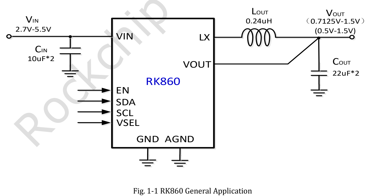
Figure 1-1. General application (English original).
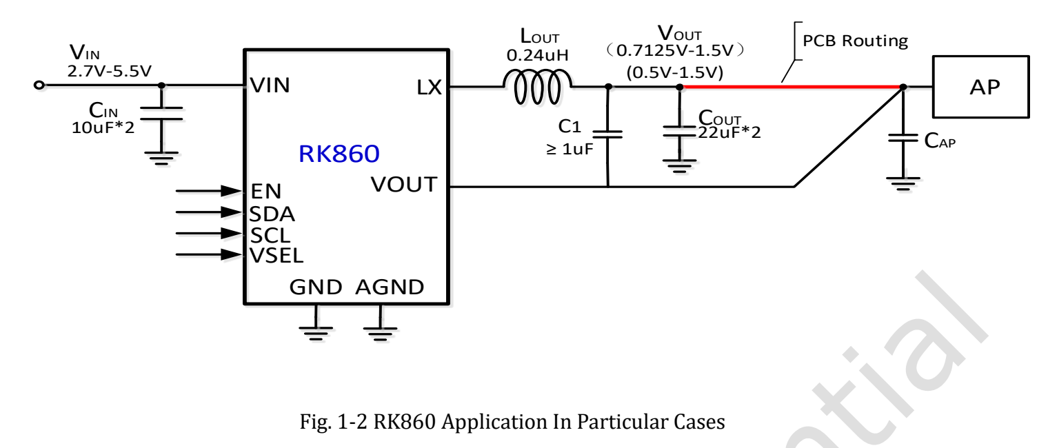
Figure 1-2. Special application with C1≥1uF, AP/CAP and PCB routing (English original).
1.4 Pin assignment
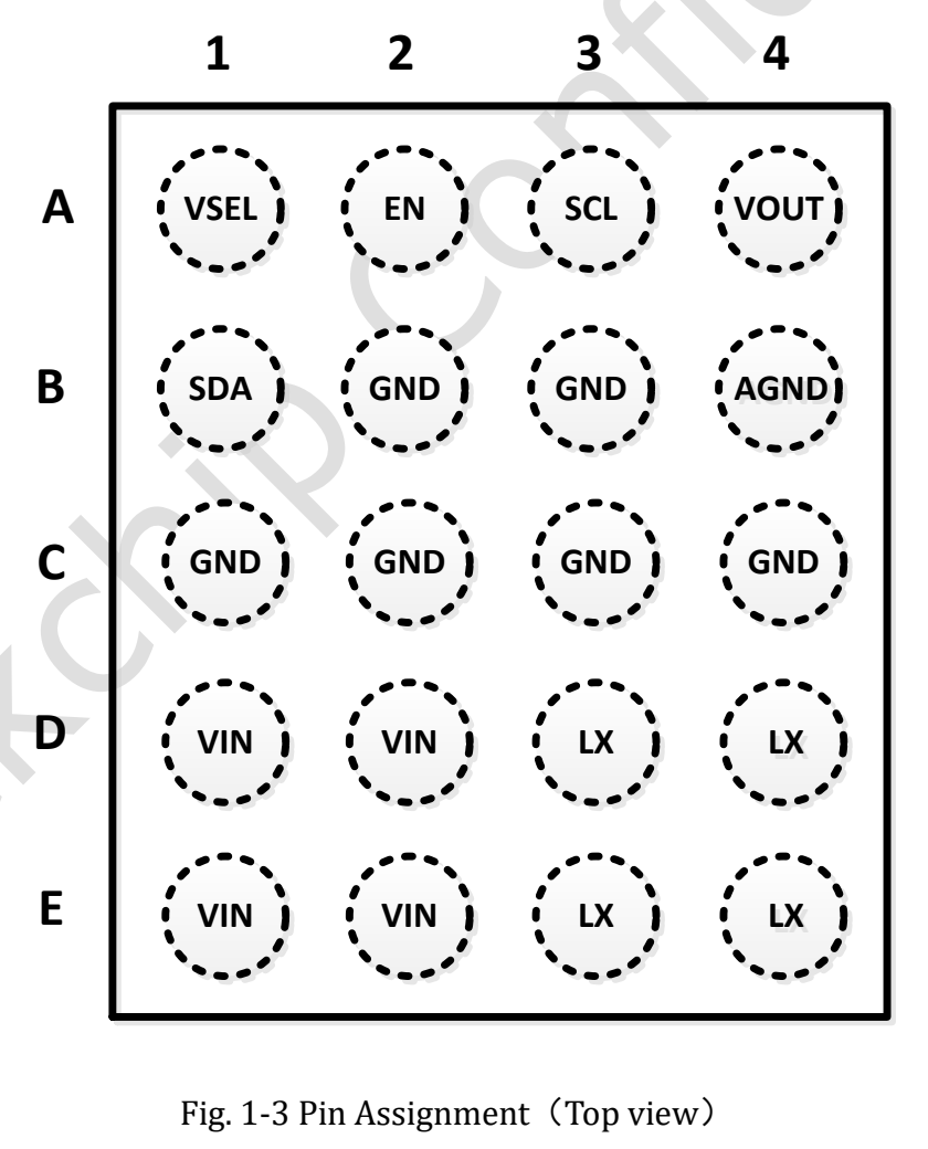
Figure 1-3. Pin assignment, top view (English original).
1.5 Pin number order
| Number | Name | Function | I/O |
|---|---|---|---|
| D1,D2,E1,E2 | VIN | Power input. Decouple to ground with at least two 10uF ceramic input-filter capacitors, placed as close as possible between VIN and GND. | Power |
| D3,D4,E3,E4 | LX | Switching node; connect to the inductor switching node. | Output |
| B2,B3,C1,C2,C3,C4 | GND | Power ground. | Ground |
| B4 | AGND | Analog ground. | |
| A1 | VSEL | Low: VOUT is set by VSEL0. High: VOUT is set by VSEL1. | Input |
| A2 | EN | Enable control, active high. Do not leave floating. | Input |
| A3 | SCL | I2C clock. | Input |
| B1 | SDA | I2C bidirectional data, open drain (source typo: “Open darin”). | I/O |
| A4 | VOUT | Output sense; connect at the output capacitor. | Output |
2. Electrical characteristics
Note 1: Exceeding absolute maximum ratings may permanently damage the device. These are stress ratings only; functional operation outside the operating specification is not implied. Prolonged exposure to absolute maximum conditions may affect reliability.
Note 2: Operation outside the recommended operating conditions is not guaranteed.
2.1 Absolute maximum ratings (Note 1)
| Parameter | Value | Unit |
|---|---|---|
| VIN pin voltage | 6.0 | V |
| Other pin voltages | VIN+0.6 | V |
| Continuous power dissipation PD @ TA=25°C, WCSP4*5-20 | 0.5 | W |
| Junction temperature TJ | -40~150 | °C |
| Lead temperature, soldering 10 sec, TSOLDER | 260 | °C |
| Storage temperature TS | -65~150 | °C |
| ESD HBM | 2000 | V |
| ESD CDM | 1000 | V |
2.2 Recommended operating conditions (Note 2)
| Parameter | Symbol | Value | Unit |
|---|---|---|---|
| Supply input voltage | VIN | 2.7~5.5 | V |
| Output voltage | VOUT | 0.5~1.5 | V |
| Inductor | L | 0.22~0.47 | uH |
| Input capacitor | CIN | >10 | uF |
| Output capacitor | COUT | 44~88 | uF |
| Junction temperature | Tj | -40~125 | °C |
| Ambient temperature | Ta | -40~85 | °C |
2.3 Electrical characteristics
Unless otherwise specified: typical application circuit, VIN=3.8V, VOUT=1.0V, L=0.24uH, COUT=22uF*2, TA=25°C. Blank cells are blank in the source; they are not zero.
| Parameter | Symbol | Condition | Min | Typ | Max | Unit |
|---|---|---|---|---|---|---|
| VIN UVLO threshold | VIN_UVLO | Vin rising | 2.55 | 2.65 | V | |
| VIN UVLO hysteresis | VIN_UVLO_HYS | Vin falling | 150 | mV | ||
| VIN OVP threshold | VIN_OV | Vin rising | 6 | V | ||
| VIN OVP hysteresis | VIN_OV_HYS | Vin falling | 200 | mV | ||
| Quiescent current | Iq | No switching, vfb=105%Vref | 70 | uA | ||
| Shutdown current | Isd | EN=L | 0.1 | uA | ||
| Software shutdown current | Isd_soft | EN=H, BUCK_EN=L | 25 | uA | ||
| Internal soft-start time | Tss | Vout=1.0V, from BUCK_EN rising edge to Vout>92% | 260 | uS | ||
| Oscillator frequency | Fclk | PWM / FPWM | 2.2 | 2.4 | 2.6 | MHz |
| Discharge resistance | Rdisc | EN=L/BUCK_EN=0 | 150 | Ω | ||
| EN/VSEL input high threshold | VIH | 1.1 | V | |||
| EN/VSEL input low threshold (source groups under high threshold) | VIL | 0.4 | V | |||
| SDA/SCL input high threshold | VIH | 1.26 | V | |||
| SDA/SCL input low threshold (source groups under high threshold) | VIL | 0.54 | V | |||
| Vout accuracy, output voltage error | VREG1 | Forced PWM, VOUT=1.0V | -0.6 | +0.6 | % | |
| Vout accuracy, output voltage error | VREG2 | Auto PFM, VOUT=1.0V | -1.5 | 1.5 | % | |
| PMOS RDS(ON) | RDS(ON)P | VIN → LX, VIN=3.8V | 24 | mΩ | ||
| NMOS RDS(ON) | RDS(ON)N | LX → GND, VIN=3.8V | 16 | mΩ | ||
| Maximum PMOS current | Ipeak | 8.5 | A | |||
| Maximum NMOS current | Ivalley | 7.0 | A | |||
| Thermal shutdown temperature | TSD | Rising threshold | 150 | °C | ||
| Thermal shutdown hysteresis | TSD_HYS | 25 | °C |
3. Chip versions
| DIE-ID | I2C-ADDR (7-bit) | Vout range / V | Default Vout / V | STEP / mV | DIE_ID |
|---|---|---|---|---|---|
| RK860-0 | 40H | 0.7125-1.5 | 1.0 | 12.5 | 0X8 |
| RK860-1 | 41H | 0.7125-1.5 | 1.0 | 12.5 | 0X8 |
| RK860-2 | 42H | 0.5-1.5 | 0.8 | 6.25 | 0XA |
| RK860-3 | 43H | 0.5-1.5 | 0.8 | 6.25 | 0XA |
4. Register description
VSEL0_A — 0x00
| Bit | Attribute | Reset | Description |
|---|---|---|---|
| 7 | RW | 0x1 | BUCK_EN0: software buck enable. 1: enable BUCK; 0: shut off. External EN low turns the regulator off; when EN is high, BUCK_EN takes precedence. |
| 6 | RW | 0x0 | MODE0: 0 allows auto-PFM at light load; 1 forces PWM. |
| 5:0 | RW | 0x17 | NSEL0: 12.5mV/step, only DIE_ID=0X8. 000000=0.7125V; 000001=0.7250V; 000010=0.7375V; …… 010111=1.0000V; …… 111111=1.5V; |
VSEL1_A — 0x01
| Bit | Attribute | Reset | Description |
|---|---|---|---|
| 7 | RW | 0x1 | BUCK_EN1: software buck enable. 1: enable BUCK-LOOP; 0: shut off. External EN low turns the regulator off; when EN is high, BUCK_EN takes precedence. |
| 6 | RW | 0x0 | MODE1: 0 allows auto-PFM at light load; 1 forces PWM. |
| 5:0 | RW | 0x17 | NSEL1: 12.5mV/step, only DIE_ID=0X8. 000000=0.7125V; 000001=0.7250V; 000010=0.7375V; …… 010111=1.0000V; …… 111111=1.5V; |
Control_Register — 0x02
| Bit | Attribute | Reset | Description |
|---|---|---|---|
| 7 | RW | 0x1 | Output Discharge: 0 disables the discharge resistor; 1 enables it. |
| 6:4 | RW | 0x0 | Slew Rate: positive voltage transition rate. 000 = 10mV/0.15us 001 = 10mV/0.3us 010 = 10mV/0.6us 011 = 10mV/1.2us 100 = 10mV/2.4us 101 = 10mV/4.8us 110 = 10mV/9.6us 111 = 10mV/19.2us |
| 3:0 | RW | 0x0 | Always reads back 0. RESET: setting to 1 resets all registers to defaults. The source does not identify a single RESET bit within 3:0; verify the implementation before writing. |
ID1 Register — 0x03
| Bit | Attribute | Reset | Description |
|---|---|---|---|
| 7:5 | R | 0x4 | VENDOR: Rockchip IC vendor code. |
| 4 | R | 0x0 | Reserved; always reads 0. |
| 3:0 | R | 0x8/0xA | DIE_ID: 0x8 means 0.7125V–1.5V at 12.5mV/step; 0xA means 0.5V–1.5V at 6.25mV/step. |
ID2 Register — 0x04
| Bit | Attribute | Reset | Description |
|---|---|---|---|
| 7:4 | R | 0x0 | Reserved; always reads 0. |
| 3:0 | R | NA | NA |
PGOOD Register — 0x05
| Bit | Attribute | Reset | Description |
|---|---|---|---|
| 7 | R | 0x0 | PGOOD: 1 means buck enabled and soft-start complete (Vout>92% of normal setting); 0 means abnormal Vout. |
| 6 | R | 0x0 | TSD: thermal buck shutdown. 1: Tdie>150°C; 0: Tdie<125°C. |
| 5 | R | 0x0 | IOVP: input overvoltage shutdown state. 1: VIN>6V; 0: VIN<5.8V. |
| 4 | R | 0x0 | UVLO: input undervoltage lockout. 1: VIN<2.4V; 0: VIN>2.55V. |
| 3:0 | R | 0x0 | Reserved. |
VSEL0_B Register — 0x06
| Bit | Attribute | Reset | Description |
|---|---|---|---|
| 7:0 | R/W | 0x30 | NSEL0: selected when VSEL=L; only DIE_ID=0XA. 00,000,000 = 0.5V 00,000,001 = 0.50625V 00,000,010 = 0.51250V …… 00,110,000 = 0.8V …… 10,100,000 = 1.5V >10,100,000 = 1.5V |
VSEL1_B Register — 0x07
| Bit | Attribute | Reset | Description |
|---|---|---|---|
| 7:0 | R/W | 0x30 | NSEL1: selected when VSEL=H; only DIE_ID=0XA. 00,000,000 = 0.5V 00,000,001 = 0.50625V 00,000,010 = 0.51250V …… 00,110,000 = 0.8V …… 10,100,000 = 1.5V >10,100,000 = 1.5V |
5. Typical performance characteristics
All curves below are source examples, not ArmSoM measurements. Preserve their operating conditions when interpreting them.
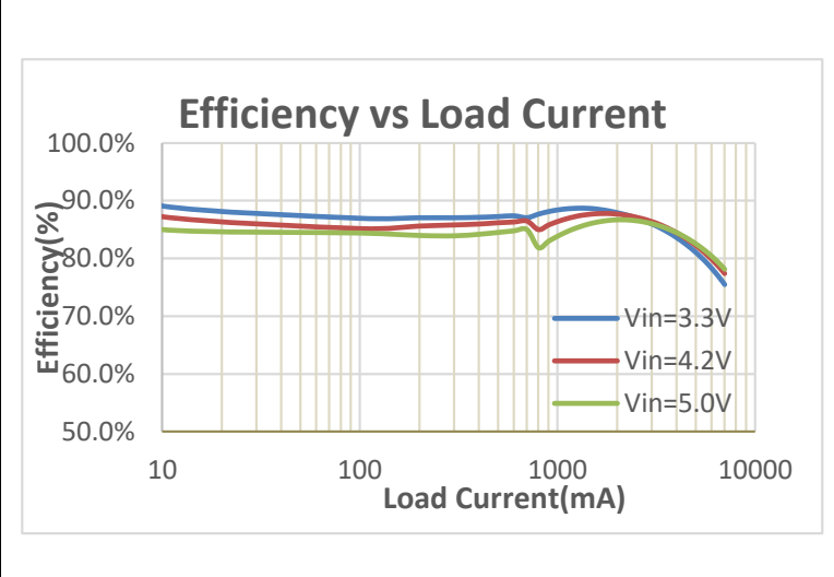
Efficiency versus load current: Vin=3.3V, 4.2V, 5.0V (English original).
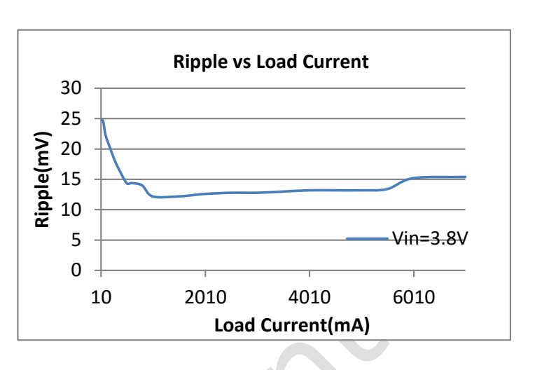
Ripple versus load current: Vin=3.8V (English original).
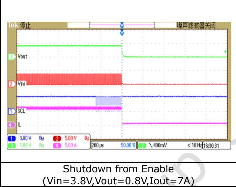
Shutdown from enable: Vin=3.8V, Vout=0.8V, Iout=7A (English original).
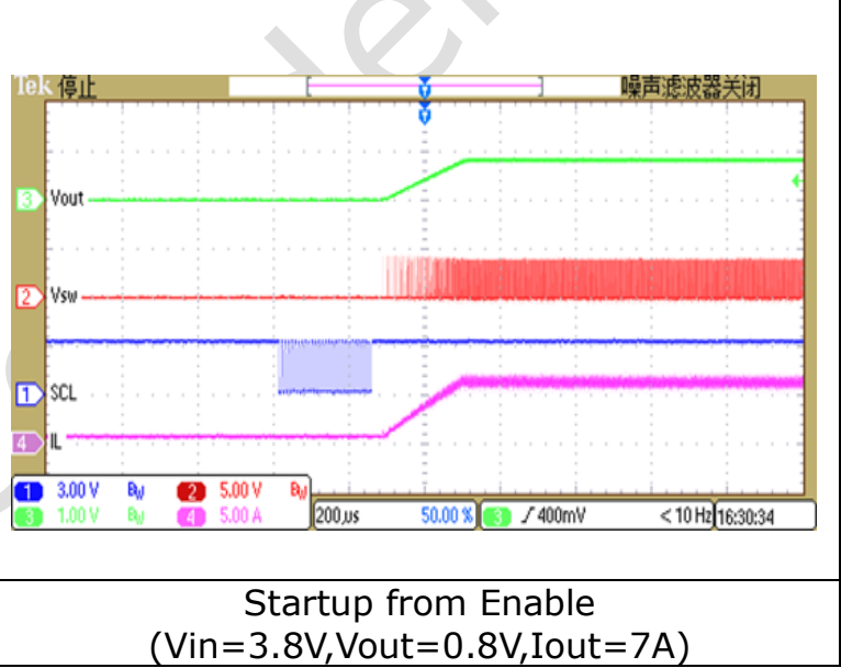
Startup from enable: Vin=3.8V, Vout=0.8V, Iout=7A (English original).
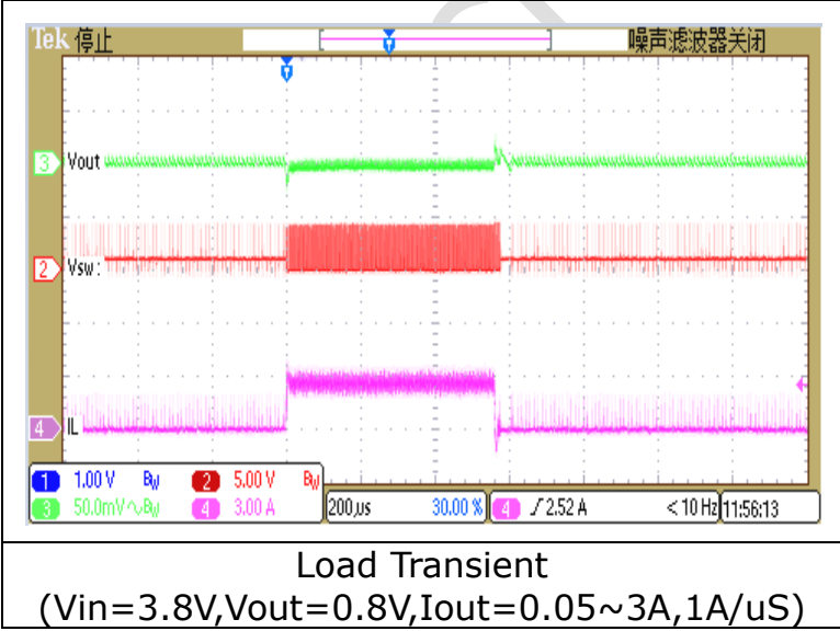
Load transient: Vin=3.8V, Vout=0.8V, Iout=0.05~3A, 1A/uS (English original).
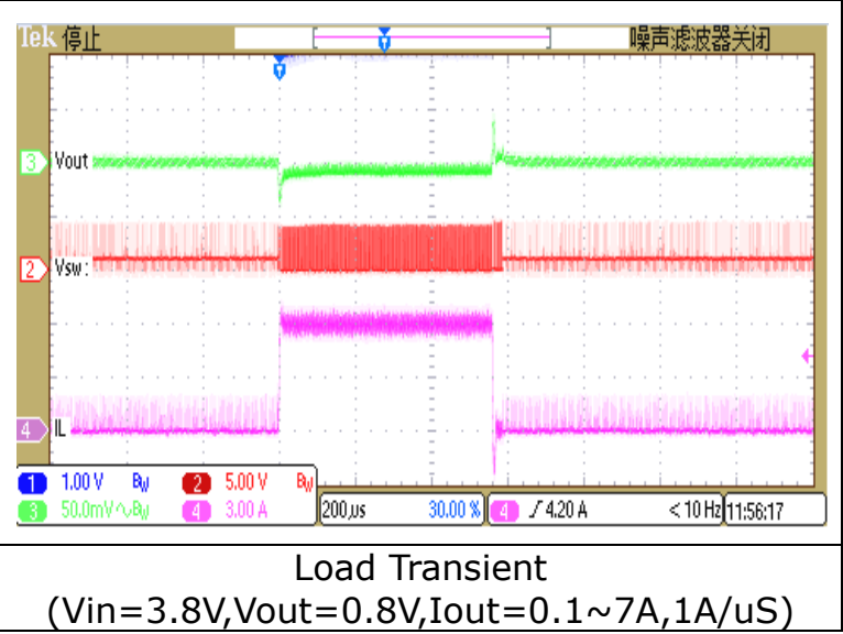
Load transient: Vin=3.8V, Vout=0.8V, Iout=0.1~7A, 1A/uS (English original).
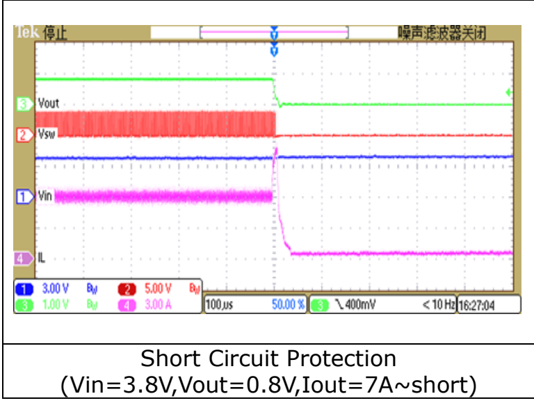
Short-circuit protection: Vin=3.8V, Vout=0.8V, Iout=7A~short (English original).
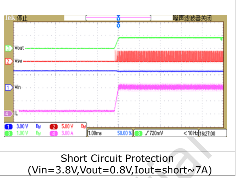
Short-circuit protection: Vin=3.8V, Vout=0.8V, Iout=short~7A (English original).
6. Package information
6.1 Ordering information
| Device | Mark | RoHS | Package | Quantity |
|---|---|---|---|---|
| RK860-0 | D0 | Pass | WLCSP20 (pitch 0.4mm) | 5000 pcs/tape |
| RK860-1 | D1 | Pass | WLCSP20 (pitch 0.4mm) | 5000 pcs/tape |
| RK860-2 | D2 | Pass | WLCSP20 (pitch 0.4mm) | 5000 pcs/tape |
| RK860-3 | D3 | Pass | WLCSP20 (pitch 0.4mm) | 5000 pcs/tape |
6.2 Top marking
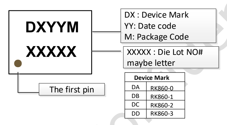
Top marking (English original). DX: device mark; YY: date code; M: package code; XXXXX: die lot number, possibly letters; first pin indicated. The diagram maps DA/DB/DC/DD to RK860-0/1/2/3, whereas the ordering table uses D0/D1/D2/D3. Verify with the supplier.
6.3 Dimensions
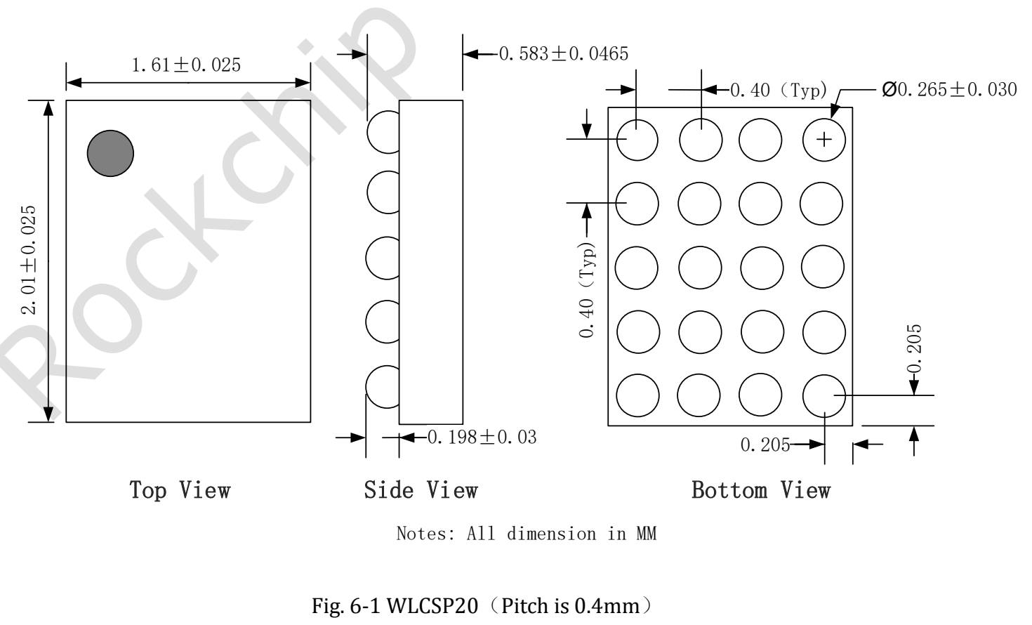
Figure 6-1. WLCSP20, 0.4mm pitch; all dimensions in mm (English original).
- Coplanarity applies to leads, corner leads and die-attach pad.
- Dimension φb applies to the metallized terminal and is measured between 0.15mm and 0.30mm from its tip. If an optional radius exists at the other end, do not measure φb in that radius area.
- A φb dimension of 0.15mm is recommended for PCB layout.
6.4 Layout recommendations
PCB routing directly affects device performance.
- Place CIN sufficiently close to the pins to minimize input interference.
- Minimize the PCB copper area associated with SW to reduce switching noise.
- Keep the feedback trace from COUT to VOUT away from SW to minimize noise coupling.
- Maximize GND-connected copper for heat dissipation and shielding. Suitable through-vias beneath the ground pad improve the circuit loop.
- Keep the GND pads of CIN, COUT and the chip on the same side, or close enough.
- For a long feedback circuit, the original text says to follow Figure 6-2: place C1 close to COUT and connect VOUT from CAP. The actual special-case layout is labelled Figure 6-4 in the body; retain this numbering discrepancy when consulting the source.
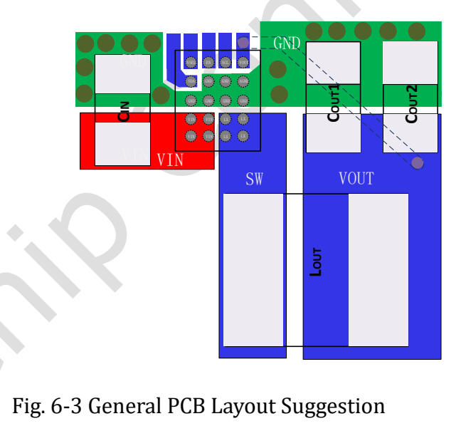
Figure 6-3. General PCB layout (English original).
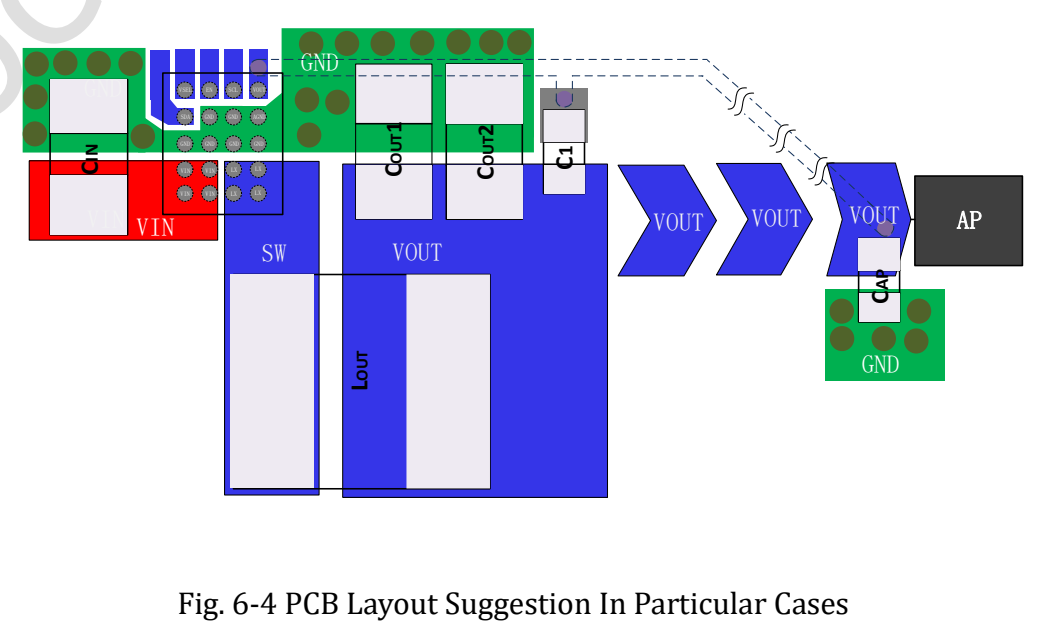
Figure 6-4. PCB layout for special cases (English original).
7. Thermal management
7.1 Overview
For reliability and operation, the absolute maximum junction temperature of RK860 must remain below 150°C. The mechanical/thermal design of a smartphone, tablet, personal navigation device or similar product, its thermal-management software and worst-case thermal applications may expose the junction to higher temperatures. Perform device-level thermal simulations using measured power for the worst-case use case.
7.2 Package thermal characteristics
The source introduction calls the following thermal-resistance table “Table 1-1”; its actual caption is Table 7-1.
| Table 7-1: WLCSP20 package | PD @ TA=25°C, WCSP4*5-20 / W | θJA, 2-layer PCB, junction to ambient / °C/W | θJC, 2-layer PCB, junction to component / °C/W |
|---|---|---|---|
| RK860 | 0.5 | 64.44 | 17.76 |
Table 7-2. SnPb eutectic process classification temperatures (TC)
| Package thickness | Volume <350 mm³ | Volume ≥350 mm³ |
|---|---|---|
| <2.5 mm | 235°C | 220°C |
| ≥2.5 mm | 220°C | 220°C |
Table 7-3. Pb-free process classification temperatures (TC)
| Package thickness | Volume <350 mm³ | Volume 350–2000 mm³ | Volume >2000 mm³ |
|---|---|---|---|
| <1.6 mm | 260°C | 260°C | 260°C |
| 1.6 mm–2.5 mm | 260°C | 250°C | 245°C |
| >2.5 mm | 250°C | 245°C | 245°C |
- The device manufacturer, but not the board assembler/user, may permit the maximum peak package-body temperature TP to exceed the values in the source references “Tables 1-2 or 1-3” (the displayed tables are 7-2 and 7-3). A higher Tp does not change classification temperature Tc.
- Package volume excludes external terminals such as balls, bumps, lands and leads, and non-integral heat sinks.
- Maximum component temperature during reflow depends on package thickness and volume. Convection reflow reduces temperature gradients between packages, but gradients caused by different SMD thermal masses can remain.
- Moisture-sensitivity levels for components intended for Pb-free assembly must be evaluated using the Pb-free classification temperatures and profiles referenced by the original as “Tables 4.2 and 1-4”, whether or not the components themselves are Pb-free. These source references are inconsistent and require verification.
- SMD packages classified to a given moisture-sensitivity level under earlier J-STD-020, JESD22-A112 (rescinded) or IPC-SM-786 (rescinded) procedures/criteria need not be reclassified unless a changed classification level or higher peak classification temperature is desired.
Table 7-4. Classification reflow profiles
| Profile feature | Sn-Pb eutectic assembly | Pb-free assembly |
|---|---|---|
| Preheat/soak minimum Tsmin | 100°C | 150°C |
| Preheat/soak maximum Tsmax | 150°C | 200°C |
| Time Tsmin to Tsmax, ts | 60–120 s | 60–120 s |
| Average ramp-up Tsmax to Tp | ≤3°C/s | ≤3°C/s |
| Liquidus temperature TL | 183°C | 217°C |
| Time at liquidus tL | 60–150 s | 60–150 s |
| Peak package-body temperature Tp* | Source: Table 1-2 (actual 7-2) | Source: Table 1-3 (actual 7-3) |
| Time tp** within 5°C of specified classification temperature Tc | 20** s | 30** s |
| Average ramp-down Tp to Tsmax | ≤6°C/s | ≤6°C/s |
| Time from 25°C to peak | ≤6 min | ≤8 min |
- The tolerance for peak profile temperature Tp is a supplier minimum and a user maximum.
** The tolerance for time at peak profile temperature Tp is a supplier minimum and a user maximum.
- Temperatures refer to the package centre on the body surface facing upward during reflow (live-bug; the source misspells it “ive-bug”). If parts are reflowed in another orientation, such as dead-bug, Tp must be within ±2°C of live-bug Tp and still meet Tc; otherwise adjust the profile. For accurate peak body-temperature measurement, consult JEP140 thermocouple recommendations.
- These profiles are for classification/preconditioning, not specifications for board assembly. Develop assembly profiles for the actual process and board design without exceeding the parameters referenced by the source as “Table 1-4” (actual Table 7-4). For example, with Tc=260°C and Tp time=30 seconds: the supplier must reach at least 260°C and spend at least 30 seconds above 255°C; the user must not exceed 260°C or 30 seconds above 255°C.
- Every component in the test load must meet the classification-profile requirements.
- SMD packages already classified to a moisture-sensitivity level under earlier J-STD-020, JESD22-A112 (rescinded) or IPC-SM-786 (rescinded) procedures/criteria need not be reclassified unless a change in classification level or a higher peak classification temperature is desired.
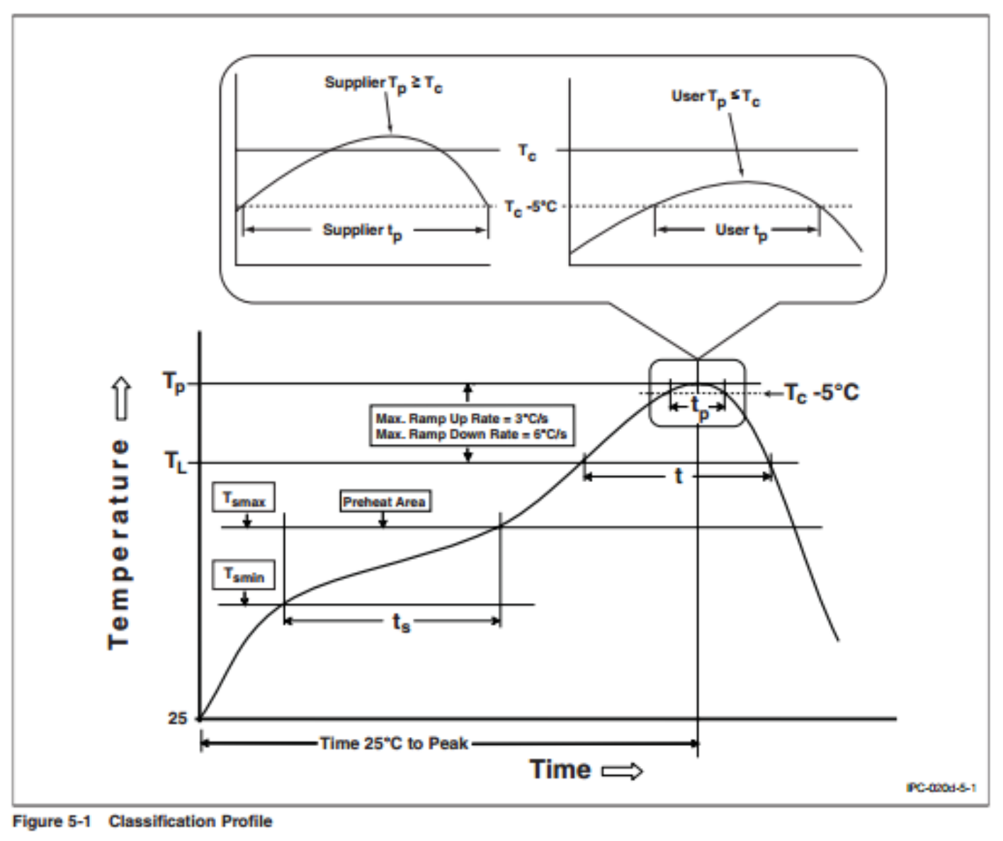
Classification profile (source caption: “Figure 5-1”, English original).
Source issues and verification boundary
- PDF p6: PFET/NFET units disagree with p10; both forms are retained above.
- PDF p6 versus p16: nominal package dimensions 1.65 × 2.05 differ from the dimension drawing 1.61±0.025 × 2.01±0.025; confirm the applicable package drawing.
- PDF p7–8 requires at least two 10uF input capacitors; p9 lists CIN>10uF. Both are preserved, not silently equated.
- PDF p12 RESET field lacks a unique bit assignment within bits 3:0.
- PDF p16: D0–D3 ordering marks versus DA–DD top-mark diagram.
- Figure/table cross-references in chapters 6–7 are inconsistent, including Figure 6-2 versus 6-4 and Tables 1-1/1-2/1-3/1-4/4.2 versus chapter-7 tables.
- Ipeak/Ivalley are described as maximum currents but their values appear in the MIN column in the original electrical table; that placement is retained.
- Register addresses, reset values, numeric limits and variant assignments have not been changed. No ArmSoM board-specific compatibility or measured result has been inferred.