
Source: RK-KF-YF-460 V2.9.0, covering chips with PCIe and Linux 4.4 or later. This is a platform reference. Verify the actual ArmSoM board SoC, PCIe wiring, SDK/BSP, kernel and peripheral. All performance tables are source-vendor EVB results, not ArmSoM measurements. Chinese uses Chinese figures; other languages use English figures. Register, firmware, power-policy and formatting examples require backed-up test hardware and validation against the actual BSP.
1. Background
1.1 Introduction
This document introduces the performance metrics related to RK PCIe applications and their testing methods, with the testing objective being to obtain the corresponding performance metrics through simple, accurate, and controllable application interfaces. The “Background” section primarily covers some of the knowledge background involved in the testing process, the “Brief Introduction to Transfer Rates” section provides theoretical calculation data for PCIe, and the remaining sections detail specific performance metrics and their testing methods.
1.2 PCIe sysfs
Linux PCIe supports the sysfs interface, which primarily provides the following resources:
/sys/devices/pci0000:17
|-- 0000:17:00.0
|   |-- class
|   |-- config
|   |-- device
|   |-- enable
|   |-- irq
|   |-- local_cpus
|   |-- remove
|   |-- resource
|   |-- resource0
|   |-- resource1
|   |-- resource2
|   |-- resource2_wc        # 64bits-pref mem resource and supports write combining, which has an optimization effect on PCIe mem to dev operations.
|   |-- revision
|   |-- rom
|   |-- subsystem_device
|   |-- subsystem_vendor
|   `-- vendor
`-- ...
For detailed reference:
2. Introduction to Transfer Rates
2.1 PCIe Bandwidth
| PCIe Generation | Encoding Scheme | Transfer Rate | x1 Lane | x2 Lane | x4 Lane | x8 Lane |
|---|---|---|---|---|---|---|
| 1.0 | 8b/10b | 2.5GT/s | 250MB/s | 500MB/s | 1GB/s | 2GB/s |
| 2.0 | 8b/10b | 5GT/s | 500MB/s | 1GB/s | 2GB/s | 4GB/s |
| 3.0 | 128b/130b | 8GT/s | 984.6MB/s | 1.969GB/s | 3.938GB/s | 7.877GB/s |
| 4.0 | 128b/130b | 16GT/s | 1.969GB/s | 3.938GB/s | 7.877GB/s | 15.754GB/s |
Transfer Rate The transfer rate is the amount of data transferred per second, GT/s, not the number of bits per second, Gbps, because the transfer amount includes overhead bits that do not provide additional throughput; for example, PCIe 1.x and PCIe 2.x use an 8b/10b encoding scheme, which occupies 20% (2/10) of the original channel bandwidth. GT/s: Giga transaction per second, which means the number of transactions per second. Gbps: Giga Bits Per Second. There is no proportional conversion relationship between GT/s and Gbps. PCIe Available Bandwidth Throughput = Transfer Rate * Encoding Scheme For example: Each Lane of the PCIe 2.0 protocol supports a rate of 58 / 10 = 4 Gbps = 500 MB/s, and for a PCIe
2.0 x8 channel, the available bandwidth for x8 is 48 = 32 Gbps = 4 GB/s.
2.2 PCIe TLP Loss
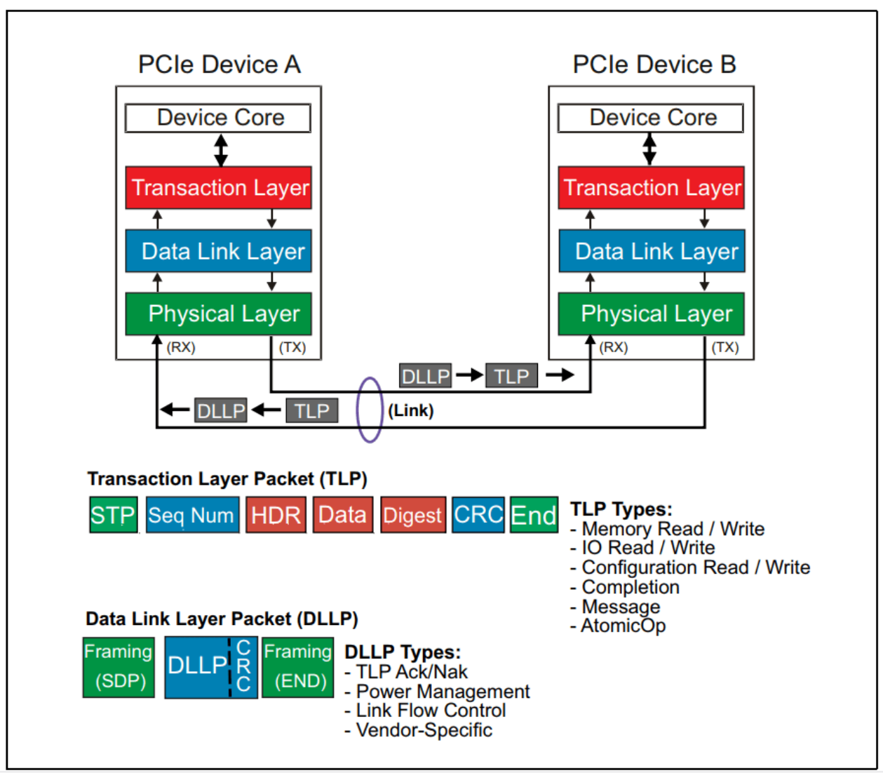
Due to the addition of packaging information after data passes through the Transaction Layer and Data Link Layer, such as packet headers, packet tails (LCRC and ECRC, etc.), packet numbering added by the data link layer, etc., the actual rate of Data Payload is lower compared to the bandwidth.
Original English figure — 8
The 28 Byte TLP overhead is the most redundant transmission packet, including the header (16 bytes), the optional ECRC (4 bytes), the LCRC (4 bytes), the sequence number (2 bytes), and the framing Symbols STP and END (2 bytes). So taking Gen3 PCIe bandwidth as an example:
| PCIe Generation | Encoding Scheme | Transfer Rate | x1 Lane | x2 Lane | x4 Lane | x8 Lane |
|---|---|---|---|---|---|---|
| 3.0 | 128b/130b | 8GT/s | 984.6MB/s | 1.969GB/s | 3.938GB/s | 7.877GB/s |
After accounting for TLP overhead:
| PCIe Generation Gen3 | x1 Lane | x2 Lane | x4 Lane | x8 Lane |
|---|---|---|---|---|
| PCIe Bandwidth (without TLP overhead) | 984.6MB/s | 1.969GB/s | 3.938GB/s | 7.877GB/s |
| 256B payload after TLP loss (256/284) | 887.5MB/s | 1.775GB/s | 3.550GB/s | 7.1002GB/s |
| 128B payload after TLP loss (128/156) | 807.8MB/s | 1.616GB/s | 3.232GB/s | 6.464GB/s |
2.3 PCIe Application Scenarios Transfer Rates
When considering the impact of factors such as DLLP for Ack/Nak and Flow Control, and Order Sets for link training and Skip on the rate, the actual data transfer rate will be even lower. In specific application scenarios, eDMA transfer is considered the optimal solution.
3. General Performance Optimization Directions
3.1 CPU and DDR Set Maximum Frequency
Please refer to the DVFS and DRAM related source code for adjustments.
3.2 CPU Shutdown Idle Strategy
Taking the RK3588 platform as an example
/* dtsi disable cpu-sleep */
--- a/arch/arm64/boot/dts/rockchip/rk3588s.dtsi
+++ b/arch/arm64/boot/dts/rockchip/rk3588s.dtsi
@@ -585,6 +585,7 @@
idle-states {
    entry-method = "psci";
    CPU_SLEEP: cpu-sleep {
        compatible = "arm,idle-state";
        local-timer-stop;
        arm,psci-suspend-param = <0x0010000>;
        entry-latency-us = <100>;
        exit-latency-us = <120>;
        min-residency-us = <1000>;
+       status = "disabled";
    };
};

/* cmdline disable ARM's default wfi, for Android platform, please modify rk3588-android.dtsi */
--- a/arch/arm64/boot/dts/rockchip/rk3588-linux.dtsi
+++ b/arch/arm64/boot/dts/rockchip/rk3588-linux.dtsi
@@ -12,7 +12,7 @@
chosen: chosen {
-               bootargs = "earlycon=uart8250,mmio32,0xfeb50000 console=ttyFIQ0 irqchip.gicv3_pseudo_nmi=0 root=PARTUUID=614e0000-0000 rw rootwait rcupdate.rcu_expedited=1 rcu_nocbs=all";
+               bootargs = "earlycon=uart8250,mmio32,0xfeb50000 console=ttyFIQ0 irqchip.gicv3_pseudo_nmi=0 root=PARTUUID=614e0000-0000 rw rootwait rcupdate.rcu_expedited=1 rcu_nocbs=all nohlt";
};
3.3 PCIe RC MPS Strategy
Refer to the “How to Configure Max Payload Size” section in the document “Rockchip_Developer_Guide_PCIe_CN.pdf”, you may attempt to configure it as pci=pcie_bus_perf . After enabling, confirm that the set MPS is a value supported by all connected PCIe devices.
3.4 PCIe Controller Bus QoS Tuning
PCIe transmission, especially DMA transmission, can occupy the bus bandwidth resources from the PCIe controller to DRAM when the throughput is increased, leading to bus contention arbitration with other IPs. In case of such extreme scenarios, the priority can be increased by modifying the PCIe controller bus QoS. Refer to the appendix “PCIe Controller QoS Tuning Registers in Various SoCs” in this document for configuration adjustments.
3.5 PCIe ASPM Tuning
The PCIe ASPM function has a certain impact on transmission performance, so it is recommended to disable the ASPM function during testing. In actual products, dynamic switching of ASPM support can be achieved in the EP function driver to ensure real-time performance by constructing test scenarios.
3.6 Adjusting CPU Policy to Reduce EP CPU Access Mapping Address Jitter
For specific scenarios where PCIe master and CPU master compete for DRAM resources, the jitter of PCIe access can be reduced by the following configurations: Adjust the SOC cache prefetch behavior on the RC side, and disable prefetching. Adjust the SOC write stream behavior on the RC side, and disable write streaming. These configurations should be modified in Trust Firmware with caution, and it should be confirmed that the overall product meets its own requirements.
3.7 Adjusting Bus Strategy to Reduce EP CPU Access Mapping Address Jitter
For applications that are sensitive to PCIe jitter behavior, consider referring to the “DRAM Scheduler Aging Adjustment for PCIe in Some SoCs” section in the appendix of this document for optimization. RK3568 Example:
io -4 -w 0xfe100010 0xff010101 # DDR timing configuration, further communication required, can be left unchanged during testing
io -4 -w 0xfe10002c 0x1 # Aging base reduced to 1, which affects all IPs
io -4 -w 0xfe100030 0x1 # The aging coefficient for the channel where PCIe is located is reduced to 1, with both base and coefficient at 1 for the fastest response speed
3.8 Monitoring Performance Jitters Caused by Abnormal PCIe Signals
Refer to the “Kernel Stability Statistics” section of the document “Rockchip_Developer_Guide_PCIe_CN.pdf” to monitor whether there are performance jitters caused by issues with PCIe signals, such as link relink or TLP replay. If there are a significant number of error packets, priority should be given to resolving signal issues before proceeding with optimization.
4. Methods to Restrict PCIe Bus Performance
When communication between PCIe devices affects other modules with high real-time requirements, such as the PCIe module of the RK3562 chip causing VOP screen flickering, the PCIe0 module of the RK3576 chip causing MIPI CSI video recording frame loss, the PCIe module of the RK3568 chip causing GMAC performance fluctuations, the PCIe module of the RK3588 chip causing SATA module performance degradation, etc., the following guidelines can be followed for individual testing: Refer to the “QoS Adjustment Registers of PCIe Controllers in Various SoCs” section in the appendix, and try to reduce the priority of memory access for the PCIe interface in reverse; Refer to the “Shaper Adjustment Registers of PCIe Controllers in Some SoCs” section in the appendix, and reduce the PCIe access granularity to see if the problem can be alleviated. Refer to the “Bandwidth Restriction Adjustment Registers of PCIe Controllers in Some SoCs” to limit the bandwidth of PCIe, improving the affected modules to meet product requirements. If the above measures are ineffective, it is possible to investigate whether there are configurations that can migrate the on-chip data access ports of the affected modules, such as some display modules (vop, vicap, etc.) which are known to have port migration capabilities. After finding the appropriate priority, shaper, and bandwidth configurations, the configuration parameters can be solidified in the product board-level dts:
- Check the “QoS Adjustment Registers of PCIe Controllers in Various SoCs” section in the appendix of this document to obtain the QoS nodes where each PCIe controller is located in the dtsi.
- The board-level dts references the corresponding QoS node and places the tested priority and bandwidth parameters, taking the RK3568 PCIe2x1 controller as an example
--- a/arch/arm64/boot/dts/rockchip/rk3568-xxx.dts
+++ b/arch/arm64/boot/dts/rockchip/rk3568-xxx.dts
@@ -2325,16 +2325,25 @@
&qos_pcie2x1{
+       /* Priority parameters */
+       priority-init = <0x202>;
+       /* Bandwidth parameters */
+       mode-init = <0x1>;
+       bandwidth-init = <0x100>;
+       saturation-init = <0x100>;
};
- The shaper node can be obtained by checking the “Shaper Adjustment Registers of PCIe Controllers in Some SoCs” section in the appendix, taking the RK3562 PCIe2x1 controller as an example
--- a/arch/arm64/boot/dts/rockchip/rk3562-xxx.dts
+++ b/arch/arm64/boot/dts/rockchip/rk3562-xxx.dts
&shaping_pcie{
+   shaping-init = <0x5>;
};
Note: For platforms whose SoC dtsi does not reserve shaping configuration nodes, it is not possible to solidify the configuration through dtsi, so please directly integrate the register configuration in the code.
5. Controller - DMA Interface Throughput
5.1 Theoretical Data Rate
DMA transfer rate theoretically approaches the rate after accounting for “PCIe TLP Loss”, with the theoretical value referenced in the “PCIe TLP Loss” section.
5.2 Test Method
5.2.1 Standard EP Testing
Testing is based on “Standard EP Function Development” + “Kernel DMATEST” testing: For Linux, refer to the relevant sections in the document Rockchip_Developer_Guide_PCIe_CN.pdf For RT-Thread, refer to the relevant sections in the document Rockchip_Developer_Guide_RT- Thread_PCIe_CN.md
5.2.2 Other Parameter Configuration
- Set high frequency for CPU and DDR
- Set PCIe RC MPS strategy to pci=pcie_bus_perf
- To improve real-time performance and accurately test DMA bandwidth, use PIO polling for DMA completion status
diff --git a/drivers/pci/controller/dwc/pcie-dw-dmatest.c b/drivers/pci/controller/dwc/pcie-dw-dmatest.c
index 4b0d4d3e01c8..df4595af962e 100644
--- a/drivers/pci/controller/dwc/pcie-dw-dmatest.c
+++ b/drivers/pci/controller/dwc/pcie-dw-dmatest.c
@@ -231,7 +231,7 @@ struct dma_trx_obj *pcie_dw_dmatest_register(struct device *dev, bool irq_en)
        }

        /* Enable IRQ transfer as default */
-       dmatest_dev->irq_en = irq_en;
+       dmatest_dev->irq_en = false;
        cur_dmatest_dev++;

        return obj;
5.3 Test Results
5.3.1 RK3568 - Standard EP Test
Test Equipment RC: RK3568-EVB1-DDR4-V10 PCIe 3.0 2 lanes ARM: 1.99G DDR: 1.5G EP: RK3568-IOTEST-DDR3-V10 PCIe 3.0 2 lanes ARM: 1.99G DDR: 1.0G Test Results
| DMA Size | 64B | 256B | 4K | 64KB | 1MB | 4MB |
|---|---|---|---|---|---|---|
| Write | 12.2MB/s | 51.7MB/s | 529.1MB/s | 941.6MB/s | 1418.2MB/s | 1454.3MB/s |
| Read | 6.0MB/s | 44.3MB/s | 442.3MB/s | 680.5MB/s | 938.9MB/s | 1080.2MB/s |
5.3.2 RK3588 - Standard EP Testing
Test Equipment RC: RK3588-EVB1-LP4X-V10 PCIe 3.0 4 lanes main core 2.4G, little core 1.8G EP: RK3588-EVB4-LP4X-V10 PCIe 3.0 4 lanes main core 2.4G, little core 1.8G
Test Results
| DMA Size | 64B | 256B | 4K | 64KB | 1MB | 4MB |
|---|---|---|---|---|---|---|
| Write | 14.7MB/S | 60.9MB/S | 660.6MB/S | 2313.4MB/S | 3026.1MB/S | 3066.1MB/s |
| Read | 13.9MB/S | 52.6MB/S | 568.7MB/S | 1490.5MB/S | 1619.8MB/S | 1660.6MB/s |
5.3.3 RK3588 Gen2x1 - Standard EP Test
Test Equipment RC: RK3588-EVB1-LP4X-V10 PCIe 3.0 4 lanes High core 2.4G Low core 1.8G EP: RK3588-EVB4-LP4X-V10 PCIe 3.0 4 lanes (downgraded to Gen2 1 lane) High core 2.4G Low core 1.8G Test Results
| DMA Size | 64B | 256B | 4K | 64KB | 1MB | 4MB |
|---|---|---|---|---|---|---|
| Write | 3.8MB/S | 14.6MB/S | 152.7MB/S | 362.6MB/S | 419.5MB/S | 427.1MB/s |
| Read | 3.8MB/S | 14.7MB/S | 146.8MB/S | 360.5MB/S | 419.2MB/S | 427.3MB/s |
Explanation: This test is for reference only. The DMA capability of the RK3588 PCIe3x4 controller should be based on the “RK3588 - Standard EP Test” section in theory.
5.3.4 RK1820 Gen2x1 - Standard EP Test
Test Equipment RC: RK3588-EVB1-LP4X-V10 PCIe 3.0 4 lanes, big core 2.4G, little core 1.8G EP: RK1820-EVB1-V10 PCIe 2.0 1 lane RK1820 SRAM Memory Test Results
| DMA Size | 64B | 256B | 4K | 64KB | 128KB | 512KB |
|---|---|---|---|---|---|---|
| Write | 10MB/S | 42MB/S | 256MB/S | 400MB/S | 422MB/s | 422MB/s |
| Read | 8MB/S | 36MB/S | 192MB/S | 310MB/S | 325MB/s | 330MB/s |
Explanation: This test is for reference only and is related to transfer bandwidth. Further testing should be combined with actual business scenarios such as chips_connect drivers. RK1820 DRAM Memory Test Results
| DMA Size | 64B | 256B | 4K | 64KB | 128KB | 512KB |
|---|---|---|---|---|---|---|
| Write | 10MB/S | 42MB/S | 256MB/S | 401MB/S | 402MB/s | 410MB/s |
| Read | 8MB/S | 36MB/S | 193MB/S | 314MB/S | 320MB/s | 323MB/s |
Explanation: This test is for reference only and is related to transfer bandwidth. Further testing should be combined with actual business scenarios such as chips_connect drivers.
6. Controller - Bar Interface Throughput
6.1 Introduction
Typically, the most common Bar access behavior for users is the Load/Store 32bits instruction, hence the metric is based on the “User Space Load/Store 32bits Instruction” test plan. This is achieved by conducting read/write tests through the pci_mmap_resource interface provided by Linux’s PCIe sysfs.
6.2 Testing APP
Refer to the appendix “resource_mmap_test.c” source code for detailed instructions, and confirm the following parameters within the source code: Select the mmap Resource with device memory attributes, for example: resource2 Compilation method for the APP, using RK3588 Android as an example:
/home1/ldq/rk-linux/prebuilts/gcc/linux-x86/aarch64/gcc-arm-10.2-2020.11-x86_64-aarch64-none-linux-gnu/bin/aarch64-none-linux-gnu-gcc -mcpu=cortex-a76 -O0 -static -DROPT -o resource_mmap_test resource_mmap_test.c
Explanation: The compilation optimization level -O0 is required to avoid the optimization of read and write commands.
6.3 Test Results
| RC | EP | Store 32bits |
Load 32bits |
|---|---|---|---|
| RK3568 PCIe 3.0 2 lanes |
RK3588 PCIe 3.0 4 lanes Big Core 2.4G Small Core 1.8G |
52.5MB/s | 3.7MB/s |
| RK3568 PCIe 2.0 1 lane |
RK3588 PCIe 3.0 4 lanes Big Core 2.4G Small Core 1.8G |
36.0MB/s | 2.4MB/s |
| RK3588 PCIe 3.0 4 lanes |
RK3588 PCIe 3.0 4 lanes Big Core 2.4G Small Core 1.8G |
53.3MB/s | 4.2MB/s |
| RK3588 PCIe 2.0 1 lane |
RK3588 PCIe 3.0 4 lanes Big Core 2.4G Small Core 1.8G |
26.7MB/s | 2.6MB/s |
| RK3528 PCIe 2.0 1 lane |
RK3588 PCIe 3.0 4 lanes Big Core 2.4G Small Core 1.8G |
67.7MB/s | 2.3MB/s |
| RK3562 PCIe 2.0 1 lane |
RK3588 PCIe 3.0 4 lanes Big Core 2.4G Small Core 1.8G |
66.3MB/s | 2.3MB/s |
| RK3572 PCIe 2.0 1 lane |
RK3588 PCIe 3.0 4 lanes Big Core 2.4G Small Core 1.8G |
67.7MB/s | 2.4MB/s |
Explanation: The test results for 64bits-pref (resource0..N) are consistent with those for 32bits-np (resource0..N).
6.4 Performance Optimization Directions
6.4.1 Increasing Data Bit Width
Introduction The bottleneck in the read/write speed of PCIe Bar is mainly due to the number of PCIe TLPs. Increasing the effective data payload of TLP can reduce the number of TLPs, which means increasing the data bit width of Load/Store requests on the bus can decrease the total number of TLPs. Common behaviors for users accessing PCIe Bar include: User mode Load/Store data bit width 32bits, actual results are based on assembly results, for example:
str w1, [x0]
User mode Load/Store SIMD data bit width 128bits This is usually the behavior after compiler optimization, for example, a SOC that supports SIMD using the -O3 compilation optimization option may achieve this, actual results are based on assembly results, for example:
str q1, [x1], #16
Kernel mode Load/Store data bit width 32bits Kernel mode memset_io/memcpy_fromio interface Test Results Taking RK3588 as an example:
| Access Behavior | Store (MB/s) | Load (MB/s) |
|---|---|---|
| User mode Load/Store 32bits | 53 | 4 |
| User mode Load/Store SIMD 128bits | 203 | 16 |
| Kernel mode Load/Store 32bits | 53 | 4 |
| Kernel mode memset_io/memcpy_fromio | 106 | 7 |
Explanation: Test Environment: RC: RK3588-EVB1-LP4X-V10 PCIe 3.0 4 lanes big core 2.4G small core 1.8G EP: RK3588-EVB4-LP4X-V10 PCIe 3.0 4 lanes big core 2.4G small core 1.8G User mode Load/Store 32bits access behavior, assembly V8-a instruction reference:
LDR <Wt>, [<Xn|SP>, (<Wm>|<Xm>){, <extend> {<amount>}}]
STR <Wt>, [<Xn|SP>, (<Wm>|<Xm>){, <extend> {<amount>}}]
User mode Load/Store SIMD 128bit access behavior, assembly V8-a instruction reference:
LDR <Qt>, [<Xn|SP>, (<Wm>|<Xm>){, <extend> {<amount>}}]
STR <Qt>, [<Xn|SP>, (<Wm>|<Xm>){, <extend> {<amount>}}]
Kernel mode Load/Store 32bits
6.4.2 Multi-threading - Ineffective
Multiple instances of resource_mmap_test.c running concurrently, reading and writing to different Bars, confirmed through a logic analyzer that the bus utilization did not increase. For actual bandwidth with no significant improvement (not exceeding 10%), the bandwidth utilization also did not increase, but indeed observed the alternating situation of TLP in different Bar spaces.
7. Controller - Interrupt Response Speed - ELBI
7.1 Introduction
The ELBI (Endpoint Local Interrupt Bypass) in DWC PCIe EP mode is implemented through the mapping of the EP (Endpoint) configuration space. The RC triggers the ELBI interrupt of the EP by writing to the ELBI mapping registers in the EP’s configuration space, thereby enhancing the responsiveness of the EP system. The response rate of ELBI interrupts primarily depends on factors such as the bus bandwidth of the EP system, the optimization level of the device driver, and the processing capability of the processor.
7.2 Testing APP
PCIe ELBI RC Endpoint Packet Sending Code
#include <linux/kthread.h>

// Create a new kernel thread to trigger ELBI interrupts
static int pcie_rkep_elbi_test_real(void *p)
{
    struct pcie_rkep *pcie_rkep = (struct pcie_rkep *)p;

    // In an infinite loop, call the rockchip_pcie_raise_elbi_irq function to trigger ELBI interrupts (using IRQ number 0)
    while(1)
        rockchip_pcie_raise_elbi_irq(pcie_rkep, 0);
}

// Use the pcie_rkep_elbi_test_real function to create a kernel thread to trigger ELBI interrupts
static int pcie_rkep_elbi_test(struct pcie_rkep *pcie_rkep)
{
    struct task_struct *tsk;

    // Use the pcie_rkep_test function to perform some test operations
    pcie_rkep_test(pcie_rkep);

    // Create a kernel thread named "rkep-elbi" and pass pcie_rkep as a parameter to the pcie_rkep_elbi_test_real function
    tsk = kthread_run(pcie_rkep_elbi_test_real, pcie_rkep, "rkep-elbi");
    if (IS_ERR(tsk)) {
        pr_err("rkep elbi start rk-pcie thread failed\n");
        return PTR_ERR(tsk);
    }

    return 0;
}
PCIe ELBI RC Endpoint Packet Sending Code Integration
 static int pcie_rkep_probe(struct pci_dev *pdev, const struct pci_device_id *id)
 {
        int ret, i;
@@ -774,6 +812,7 @@ static int pcie_rkep_probe(struct pci_dev *pdev, const struct pci_device_id *id)
                 pcie_rkep->obj_info->version);

        device_create_file(&pdev->dev, &dev_attr_rkep);
+       pcie_rkep_elbi_test(pcie_rkep);

        return 0;
 err_register_obj:
PCIe ELBI EP Endpoint Speed Measurement Code
#include <linux/kthread.h>

// Create a new kernel thread to measure the triggering frequency of ELBI interrupts
static int pcie_rkep_elbi_test_real(void *p)
{
    struct rockchip_pcie *rockchip = (struct rockchip_pcie *)p;
    int cur_count, last_count = rockchip->elbi_count;
    u64 us = 0;

    // In an infinite loop, perform the following operations every 1 second
    while(1) {
        msleep(1000); // Wait for 1 second

        // Get the current ELBI interrupt count
        cur_count = rockchip->elbi_count;

        // If the current interrupt count is not 0, calculate the time interval between the last and current interrupt counts (in microseconds)
        if (cur_count) {
            us = 1000000 / (cur_count - last_count);
        }

        // Print the current ELBI interrupt count and triggering frequency
        pr_err("elbi count=%d %lluus\n", cur_count, us);

        // Update the last interrupt count
        last_count = rockchip->elbi_count;
    }
}

// Use the pcie_rkep_elbi_test_real function to create a kernel thread to measure the triggering frequency of ELBI interrupts
static __maybe_unused int pcie_rkep_elbi_test(struct rockchip_pcie *rockchip)
{
    struct task_struct *tsk;
    // Create a kernel thread named "rkep-elbi" and pass rockchip as a parameter to the pcie_rkep_elbi_test_real function
    tsk = kthread_run(pcie_rkep_elbi_test_real, rockchip, "rkep-elbi");
    if (IS_ERR(tsk)) {
        pr_err("rkep elbi start rk-pcie thread failed\n");
        return PTR_ERR(tsk);
    }

    return 0;
}
PCIe ELBI EP Endpoint Speed Measurement Code Integration
 static int rockchip_pcie_ep_probe(struct platform_device *pdev)
 {
        struct device *dev = &pdev->dev;
@@ -1276,6 +1316,7 @@ static int rockchip_pcie_ep_probe(struct platform_device *pdev)
                goto deinit_phy;

        rockchip_pcie_add_misc(rockchip);
+       pcie_rkep_elbi_test(rockchip);

        return 0;
7.3 Test Results
| RC | EP | Default Latency (us) |
|---|---|---|
| RK3568-EVB1-DDR4-V10 PCIe 3.0 2 lanes ARM: 1.99G DDR: 1.5G |
RK3568-IOTEST-DDR3-V10 PCIe 3.0 2 lanes ARM: 1.99G DDR: 1.0G |
6 |
| RK3588-EVB1-LP4X-V10 PCIe 3.0 4 lanes Big Core 2.4G Little Core 1.8G |
RK3588-EVB4-LP4X-V10 PCIe 3.0 4 lanes Big Core 2.4G Little Core 1.8G |
6 |
Explanation: Please note that the specific implementation and application scenarios may vary depending on system configuration, hardware platform, and driver requirements.
7.4 Performance Optimization Direction
The ELBI interrupt response rate mainly depends on factors such as the EP system bus bandwidth, the optimization level of device drivers, and the processing capability of the processor. Taking RK3588 as an example:
| Model | Default Latency (us) |
Register Read/Write Rate (us/s) |
CPU_SLEEP Mode Disabled Latency (us) |
CPU Fixed Frequency Maximum Frequency Latency (us) |
|---|---|---|---|---|
| RK3588 | 6 | 2 | 6 | 4 |
Explanation: Register Read/Write Rate: The maximum rate at which the RC initiates an ELBI request by calling the ELBI write config interface. However, the actual response rate obtained due to the EP’s interrupt scheduling response time will be lower than this result.
8. Controller - Interrupt Response Speed - MSI
8.1 Introduction
MSI (Message Signaled Interrupt) is a type of interrupt transmission mechanism in PCIe. MSI triggers interrupts by sending interrupt messages to specific message addresses. Each device can have multiple message addresses, with each address corresponding to an interrupt. This enables parallel processing of interrupt requests, significantly improving response speed and system performance. The MSI interrupt response rate depends on factors such as the bandwidth of the RC system bus, the optimization level of device drivers, and the processing capabilities of the processor. Generally speaking, systems using the MSI interrupt mechanism can significantly reduce interrupt latency and maintain good response rates even under high load conditions.
8.2 Test APP
PCIe MSI EP Endpoint Packet Transmission Code
#include <linux/kthread.h>

// PCIe MSI RC and EP endpoint example code

static int pcie_rkep_elbi_test_real(void *p)
{
    struct rockchip_pcie *rockchip = (struct rockchip_pcie *)p;

    // EP endpoint continuously sends MSI interrupts to the RC endpoint
    while(1) {
        rockchip_pcie_raise_msi_irq(rockchip, 0);
    }
}

static int pcie_rkep_elbi_test(struct rockchip_pcie *rockchip)
{
    struct task_struct *tsk;

    // Create a kernel thread to execute the pcie_rkep_elbi_test_real function
    tsk = kthread_run(pcie_rkep_elbi_test_real, rockchip, "rkep-elbi");

    // Check if the thread creation was successful
    if (IS_ERR(tsk)) {
        pr_err("Failed to start rkep elbi thread\n");
        return PTR_ERR(tsk);
    }

    return 0;
}
PCIe MSI EP Endpoint Packet Transmission Code Integration
 static int pcie_rkep_probe(struct pci_dev *pdev, const struct pci_device_id *id)
 {
        int ret, i;
@@ -774,6 +812,7 @@ static int pcie_rkep_probe(struct pci_dev *pdev, const struct pci_device_id *id)
                 pcie_rkep->obj_info->version);

        device_create_file(&pdev->dev, &dev_attr_rkep);
+       pcie_rkep_elbi_test(pcie_rkep);

        return 0;
 err_register_obj:
PCIe MSI RC Endpoint Speed Measurement Code
#include <linux/kthread.h>

static int pcie_rkep_elbi_test_real(void *p)
{
    struct pcie_rkep *pcie_rkep = (struct pcie_rkep *)p;
    int cur_count, last_count = pcie_rkep->msi_count;
    u64 us = 0;

    // Execute in an infinite loop, printing the current msi_count value and the time interval between two prints once per second
    while(1) {
        msleep(1000);
        cur_count = pcie_rkep->msi_count;
        if (cur_count) {
            us = 1000000 / (cur_count - last_count); // Calculate the time interval (microseconds)
        }
        pr_err("msi count=%d %lluus\n", cur_count, us); // Print msi_count and time interval
        last_count = pcie_rkep->msi_count;
    }
    return 0;
}

static __maybe_unused int pcie_rkep_elbi_test(struct pcie_rkep *pcie_rkep)
{
    struct task_struct *tsk;

    tsk = kthread_run(pcie_rkep_elbi_test_real, pcie_rkep, "rkep-elbi"); // Create a kernel thread to execute the pcie_rkep_elbi_test_real function
    if (IS_ERR(tsk)) {
        pr_err("rkep elbi start rk-pcie thread failed\n");
        return PTR_ERR(tsk);
    }

    return 0;
}
PCIe MSI RC Endpoint Speed Measurement Code Invocation Reference
 static int pcie_rkep_probe(struct pci_dev *pdev, const struct pci_device_id *id)
 {
        int ret, i;
@@ -774,6 +812,7 @@ static int pcie_rkep_probe(struct pci_dev *pdev, const struct pci_device_id *id)
                 pcie_rkep->obj_info->version);

        device_create_file(&pdev->dev, &dev_attr_rkep);
+       pcie_rkep_elbi_test(pcie_rkep);

        return 0;
 err_register_obj:
8.3 Test Results
| RC | EP | Default Latency (us) |
|---|---|---|
| RK3568-EVB1-DDR4-V10 PCIe 3.0 2 lanes ARM: 1.99G DDR: 1.5G |
RK3568-IOTEST-DDR3-V10 PCIe 3.0 2 lanes ARM: 1.99G DDR: 1.0G |
2 |
| RK3588-EVB1-LP4X-V10 PCIe 3.0 4 lanes Big Core 2.4G Little Core 1.8G |
RK3588-EVB4-LP4X-V10 PCIe 3.0 4 lanes Big Core 2.4G Little Core 1.8G |
2 |
Explanation: Please note that the specific implementation and application scenarios may vary depending on system configuration, hardware platform, and driver requirements.
8.4 Performance Optimization Direction
The optimization direction for MSI rate is consistent with the ELBI interrupt optimization direction, for detailed reference, please refer to the section “Controller - Interrupt Response Rate - ELBI”.
9. Controller - Peripheral CPU Access Mapping Address Response Rate
9.1 Introduction
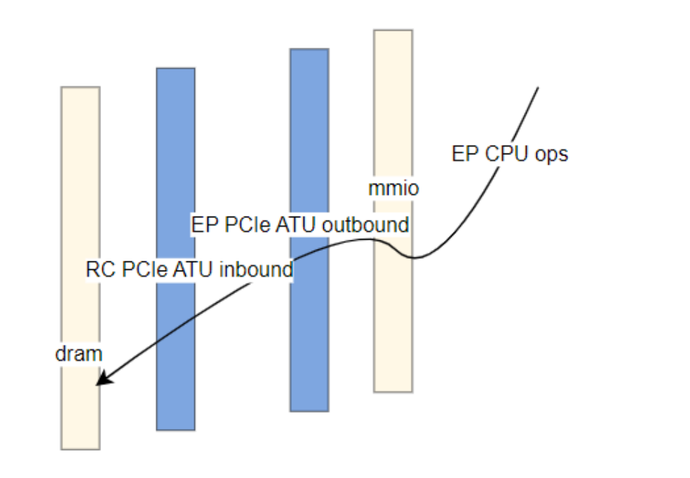
PCIe supports initiating CPU access behavior from the RC side through the Bar Interface to read and write peripheral data, and also supports initiating CPU access behavior from the EP side through mapped addresses to read and write data on the RC side.
Original English figure — 24
9.2 Test APP
Introduction to Testing Set the outbound for RK3588 EP, use the CPU to access the outbound address, and complete a cycle of write followed by read, repeating this cycle 10,000 times. Test Commands RC: Set high frequency for CPU/DRAM, by default without adding additional loads, add corresponding loads according to your product scenario.
EP: The test_memory under u-boot, EP test command reference:
#define TEST_ITERATIONS 3000000

#define TEST_RECORD_LENGTH 256
static uint32_t record[TEST_RECORD_LENGTH];
static volatile uint32_t value;
static uint32_t max_duration;
static uint32_t total_duration;
static uint32_t loops;

void test_memory(volatile uint32_t *address) {
    ulong duration;

    int i;

    printf("Memory write-read test starting...\n");

    for (i = 0; i < TEST_ITERATIONS; i++) {
        // Get start time
        duration = get_ticks();

        // Write to memory
        *address = 0x12345678;

        // Read from memory
        value = *address;

        // Get end time
        duration = get_ticks() - duration;

        // Update maximum duration
        if (duration > max_duration) {
            max_duration = duration;
        }

        // Accumulate total duration
        total_duration += duration;
        //printf("Iteration %d: %lu ticks\n", i + 1, duration);
        record[duration]++;
    }

    // Calculate average duration
    uint32_t average_duration = total_duration / (loops * TEST_ITERATIONS);

    printf("Maximum duration: %u ticks %lu us\n", max_duration, max_duration / (gd->arch.timer_rate_hz / 1000000));
    printf("Average duration: %u ticks %lu us\n", average_duration, average_duration / (gd->arch.timer_rate_hz / 1000000));
    printf("ticks - count (24tick/1us)\n");
    for (i = 0; i < TEST_RECORD_LENGTH; i++) {
        if (record[i])
            printf("%d - %d\n", i, record[i]);
    }
}

static int main(void)
{
        printf("mmio mem\n");
        memset(record, 0, 4 * TEST_RECORD_LENGTH);
        max_duration = 0;
        total_duration = 0;
        for (loops = 1; loops < 1000; loops++) {
            test_memory((volatile u32 *)(0xf0000000));
        }
    }
}
9.3 Test Results
9.3.1 RK3566 Gen2x1
Basic Environment Devices RC: RK_EVB_3566_LP4X_V10 default PCIe Gen2x1 mps 128B EP: RK3588 EVB1 PCIe Gen3x4 Test Results
| Description | avg(us) | max(us) |
|---|---|---|
| Basic Test | 1.7 | 2.3 |
| DRAM Load Test | 1.9 | 7.9 |
Notes: RC has no DRAM load, EP CPU access to PCIe mapped space has minimal jitter. RC has DRAM load, EP CPU access to PCIe mapped space has significant jitter. Common optimization directions for such issues include: Refer to the section “Adjusting CPU Policies to Reduce EP CPU Access Jitter to Mapped Addresses” Refer to the section “Adjusting Bus Policies to Reduce EP CPU Access Jitter to Mapped Addresses” RC DRAM load test includes Bit Flip and Reversed Mem tests.
10. Peripherals - NVMe Throughput
10.1 Testing Method
10.1.1 fio Simulation of CrystalMark
| Test Item |
Subitem | Test Command | Unit |
|---|---|---|---|
| SEQ1M Q32T1 READ |
adb shell ./data/fio -filename=/mnt/test -direct=1 -iodepth 32 -thread -rw=read -ioengine=libaio -bs=1024K -size=10G -numjobs=1 -runtime=180 -group_reporting -name=read_seq_1024k_q32_t1 | MB/s | |
| SEQ1M Q32T1 WRITE |
adb shell ./data/fio -filename=/mnt/test -direct=1 -iodepth 32 -thread -rw=write -ioengine=libaio -bs=1024K -size=10G -numjobs=1 -runtime=180 -group_reporting -name=write_seq_1024k_q32_t1 | MB/s | |
| RND4K Q32T1 READ |
Throughput | adb shell ./data/fio -filename=/mnt/test -direct=1 -iodepth 32 -thread -rw=randread -ioengine=libaio -bs=4K -size=4G -numjobs=1 -runtime=180 -group_reporting -name=read_rand_4k_q32_t1 | MB/s K(IOPS) |
| RND4K Q32T1 WRITE |
Throughput | adb shell ./data/fio -filename=/mnt/test -direct=1 -iodepth 32 -thread -rw=randwrite -ioengine=libaio -bs=4K -size=4G -numjobs=1 -runtime=180 -group_reporting -name=write_rand_4k_q32_t1 | MB/s K(IOPS) |
Explanation: If the test environment does not have libaio installed, psync can be used as an alternative psync uses a synchronous method to simulate concurrent bulk submission of IO requests to the kernel with multiple threads libaio employs Kernel Native AIO, which can submit IO requests to the kernel in bulk at once. Compared to psync, it has lower overhead, better performance, and is more suitable for evaluating NVMe performance. Creating ext4 online, using the Linux system as an example:
mkfs.ext4 /dev/nvme0n1
mount -t ext4 /dev/nvme0n1 /mnt
Creating f2fs online, using the Android system as an example:
make_f2fs /dev/block/nvme0n1
mount -t f2fs -o fsync_mode=nobarrier /dev/block/nvme0n1 /mnt
10.2 Test Results
10.2.1 RK3568 Gen3x2
Host Overview RK3568 EVB1 PCIe Gen3x2 controller The bottleneck of Gen3x2 PCIe transfer rate is primarily in the PCIe controller, hence the test equipment CPU/DDR parameters use default configurations Peripherals Samsung 980 M.2 NVMe SSD 1TB PCIe Gen3x4 fio simulation CrystalDiskMark 8.0.1 Test Results
| APP Test Name | Transfer Rate MB/s | IOPS (K) |
|---|---|---|
| SEQ1M Q32T1 READ | 1510 | \ |
| SEQ1M Q32T1 WRITE | 1488 | \ |
| RND4K Q32T1 READ | 152 | 40 |
| RND4K Q32T1 WRITE | 145 | 37 |
10.2.2 RK3588 Gen3x4
Host Overview RK3588 EVB1 PCIe Gen3x4 Host Controller Port0/1 x4 RC Fixed frequency big core 2.4G, little core 1.8G, mq-deadline, f2fs nobarrier, LPDDR4X, 2112MHz Peripherals Samsung 980 M.2 NVMe SSD 1TB PCIe Gen3x4 PC CrystalDiskMark Test Results:
| PC CrystalMark 8.0.1 | Transfer Rate MB/s | IOPS (K) |
|---|---|---|
| SEQ1M Q32T1 READ | 3222 | \ |
| SEQ1M Q32T1 WRITE | 2600 | \ |
| RND4K Q32T1 READ | 708 | \ |
| RND4K Q32T1 WRITE | 486 | \ |
fio Simulated CrystalMark 8.0.1 Test Results
| APP Test Name | Transfer Rate MB/s | IOPS (K) |
|---|---|---|
| SEQ1M Q32T1 READ | 3219.2 | \ |
| SEQ1M Q32T1 WRITE | 3108.7 | \ |
| RND4K Q32T1 READ | 794 | 203 |
| RND4K Q32T1 WRITE | 647 | 165 |
10.2.3 RK3588 Gen3x2
Host Overview RK3588 EVB1 PCIe3x4 Host Controller Port0 x2 RC Fixed-frequency big core 2.4G, little core 1.8G, mq-deadline, f2fs nobarrier, LPDDR4X, 2112MHz Peripherals PHISON 128G BGA SSD PC CrystalDiskMark Test Results:
| CrystalMark 8.0.1 | Transfer Rate MB/s | IOPS (K) |
|---|---|---|
| SEQ1M Q32T1 READ | 1615 | \ |
| RND4K Q32T1 READ | 434 | \ |
| SEQ1M Q32T1 WRITE | 626 | \ |
| RND4K Q32T1 WRITE | 230 | \ |
fio Simulated CrystalMark 8.0.1 Test Results
| APP Test Name | Transfer Rate MB/s | IOPS (K) |
|---|---|---|
| SEQ1M Q32T1 READ | 1572.4 | \ |
| SEQ1M Q32T1 WRITE | 600 | \ |
| RND4K Q32T1 READ | 422 | 101 |
| RND4K Q32T1 WRITE | 355 | 90 |
10.2.4 RK3588s Gen2x1
Host Overview RK3588s EVB1 PCIe2x1l1 Host Controller Port0 x1 RC Fixed-frequency big core 2.4G, little core 1.8G, mq-deadline, f2fs nobarrier, LPDDR4X, 2112MHz
Peripherals PHISON 128G BGA SSD. fio Simulation CrystalDiskMark 8.0.1 Test Results
| APP Test Name | Transfer Rate MB/s | IOPS (K) |
|---|---|---|
| SEQ1M Q32T1 READ | 407 | \ |
| SEQ1M Q32T1 WRITE | 350 | \ |
| RND4K Q32T1 READ | 400 | 102 |
| RND4K Q32T1 WRITE | 134 | 32 |
10.2.5 RK3528 Gen2x1
Host Overview RK3528 EVB2 PCIe Gen2x1 controller The bottleneck of Gen2x1 PCIe transfer rate is entirely within the PCIe controller, hence the test device CPU/DDR and other parameters use default configurations. Peripherals Samsung 980 M.2 NVMe SSD 1TB PCIe Gen3x4 fio Simulation CrystalDiskMark 8.0.1 Test Results
| APP Test Name | Transfer Rate MB/s | IOPS (K) |
|---|---|---|
| SEQ1M Q32T1 READ | 410 | \ |
| SEQ1M Q32T1 WRITE | 392 | \ |
| RND4K Q32T1 READ | 327 | 83 |
| RND4K Q32T1 WRITE | 300 | 76 |
10.2.6 RK3562 Gen2x1
Host Overview RK3562 EVB1 PCIe Gen2x1 host controller The bottleneck of Gen2x1 PCIe transfer rate is entirely within the PCIe controller, hence the test equipment CPU/DDR and other parameters use the default configuration. Peripherals Samsung 980 M.2 NVMe SSD 1TB PCIe Gen3x4
fio Simulation CrystalDiskMark 8.0.1 Test Results
| APP Test Name | Transfer Rate MB/s | IOPS (K) |
|---|---|---|
| SEQ1M Q32T1 READ | 409 | \ |
| SEQ1M Q32T1 WRITE | 391 | \ |
| RND4K Q32T1 READ | 343 | 85 |
| RND4K Q32T1 WRITE | 253 | 63 |
10.2.7 RK3576 Gen2x1
Host Overview RK3576 EVB1 PCIe 2x1 controller The bottleneck of Gen2x1 PCIe transfer rate is entirely within the PCIe controller, hence the test equipment CPU/DDR and other parameters use default configurations. Peripherals Samsung 980 M.2 NVMe SSD 1TB PCIe Gen3x4 fio Simulation CrystalDiskMark 8.0.1 Test Results
| APP Test Name | Transfer Rate MB/s | IOPS (K) |
|---|---|---|
| SEQ1M Q32T1 READ | 397 | \ |
| SEQ1M Q32T1 WRITE | 391 | \ |
| RND4K Q32T1 READ | 313 | 78 |
| RND4K Q32T1 WRITE | 255 | 63 |
11. Appendix
11.1 PCIe Controller QoS Tuning Registers in Various SoCs
The register command examples in the table below are configured for the highest priority allowed; please adjust according to test conditions as needed.
| Chip | Controller | Register Command | Node in dtsi |
|---|---|---|---|
| RK1808 | pcie0 | io -4 0xfe880008 0x303 | qos_pcie |
| RK3528 | pcie2x1 | io -4 0xff280188 0x404 | qos_pcie |
| RK3562 | pcie2x1 | io -4 0xfeea0008 0x404 | qos_pcie |
| RK3566 RK3568 |
pcie2x1 | io -4 0xfe190008 0x80000303 | qos_pcie2x1 |
| RK3566 RK3568 |
pcie3x1 | io -4 0xfe190088 0x80000303 | qos_pcie3x1 |
| RK3566 RK3568 |
pcie3x2 | io -4 0xfe190108 0x80000303 | qos_pcie3x2 |
| RK3576 | pcie0 | io -4 0x27f0a008 0x303 | qos_mmu0 |
| RK3576 | pcie1 | io -4 0x27f0a088 0x303 | qos_mmu1 |
| RK3588 | PCIe1L0/1/2 | io -4 0xfdf3a008 0x404 | qos_gic600_m0 |
| RK3588 | PCIe3x4 PCIe3x2 | io -4 0xfdf3a208 0x404 | qos_gic600_m1 |
11.2 PCIe Controller Shaper Adjustment Registers in Some SoCs
The following table lists the chips that currently have shaper adjustment registers, with the command example set to the maximum allowed access granularity (i.e., 0xff). The allowed configurable values range from 0x1 to 0xff, with smaller values indicating finer granularity. Adjustments should be made based on actual testing conditions.
| Chip | Controller | Register Command | Shaping Node in dtsi |
|---|---|---|---|
| RK3562 | pcie2x1 | io -4 0xfeea0088 0xff | shaping_pcie |
| RK3576 | pcie0 | io -4 0x27f0a108 0xff | None |
| RK3576 | pcie1 | io -4 0x27f0a188 0xff | None |
| RK3588 | PCIe1L0/1/2 | io -4 0xfdf3a088 0xff | None |
| RK3588 | PCIe3x4 PCIe3x2 | io -4 0xfdf3a288 0xff | None |
11.3 PCIe Controller Bandwidth Limit Adjustment Registers in Some SoCs
The value allows configuration of a range from 0 to 0x1ff, where a smaller value indicates a lower limitation on PCIe bandwidth.
| Chip | Controller | Register Command |
|---|---|---|
| RK3562 | pcie2x1 | io -4 0xfeea000c 0x1 io -4 0xfeea0010 value io -4 0xfeea0014 value |
| RK3566 RK3568 |
pcie2x1 | io -4 0xfe19000c 0x1 io -4 0xfe190010 value io -4 0xfe190014 value |
| RK3566 RK3568 |
pcie3x1 | io -4 0xfe19008c 0x1 io -4 0xfe190090 value io -4 0xfe190094 value |
| RK3566 RK3568 |
pcie3x2 | io -4 0xfe19010c 0x1 io -4 0xfe190110 value io -4 0xfe190114 value |
| RK3576 | pcie0 | io -4 0x27f0a00c 0x1 io -4 0x27f0a010 value io -4 0x27f0a014 value |
| RK3576 | pcie1 | io -4 0x27f0a08c 0x1 io -4 0x27f0a090 value io -4 0x27f0a094 value |
| RK3588 | PCIe1L0/1/2 | io -4 0xfdf3a00c 0x1 io -4 0xfdf3a010 value io -4 0xfdf3a014 value |
| RK3588 | PCIe3x4 PCIe3x2 | io -4 0xfdf3a20c 0x1 io -4 0xfdf3a210 value io -4 0xfdf3a214 value |
11.4 PCIe-Related DRAM Scheduler Aging Adjustments in Some SoCs
| Chip | Controller | Register Command |
Remarks |
|---|---|---|---|
| RK3568 | PCIe2x1/PCIe3x2/PCIe3x1 | io -4 0xfe10002c 0x1 io -4 0xfe100030 0x1 |
Aging0 of pipe to DDR needs adjustment |
| RK3588(S) | PCIe1L0/1/2 | io -4 0xfe00002c 0x1 io -4 0xfe00003c 0x1 io -4 0xfe00202c 0x1 io -4 0xfe00203c 0x1 io -4 0xfe00402c 0x1 io -4 0xfe00403c 0x1 io -4 0xfe00602c 0x1 io -4 0xfe00603c 0x1 |
All four channels’ port3 (aging3) need adjustment |
| RK3588(S) | PCIe3x4 PCIe3x2 | io -4 0xfe00002c 0x1 io -4 0xfe000038 0x1 io -4 0xfe00202c 0x1 io -4 0xfe002038 0x1 io -4 0xfe00402c 0x1 io -4 0xfe004038 0x1 io -4 0xfe00602c 0x1 io -4 0xfe006038 0x1 |
All four channels’ port2 (aging2) need adjustment |