
ArmSoM applicability and source scope
This is a Rockchip platform reference, not an ArmSoM hardware test report. The source is Rockchip_Driver_Guide_VI_EN_v1.1.5.pdf, V1.1.5, 230 PDF pages (the last page is blank). No Chinese PDF was supplied. Chinese and Russian translate this English source in full and use its original English figures. All measurements, commands and logs are source examples; no board-specific hardware validation was performed.
The source product table and applicability matrix below differ in scope. The body additionally discusses RK3588/RK3588S and RV1106. ArmSoM Sige7 is officially documented as an RK3588 board with camera usage, but that does not verify compatibility with this source’s legacy SDK, kernel drivers or APIs. Before adaptation, check the exact board and SoC, vendor SDK/BSP and kernel (4.19 or 5.10 as specified), sensor, lane routing, power, clock, DTS, ISP/VICAP topology and IQ/AIQ versions.
This V1.1.5 edition is separate from the existing V1.0.7 article. Both the newer CIS chapter 8 and repeated CIS chapter 10 are retained, including their differences. Source inconsistencies such as differing RK356x limits, node spellings, reset descriptions and exposure formulas are recorded rather than silently corrected. Memory/IOMMU/clock optimization examples require target-specific validation.
Editorial notes · Previous V1.0.7 reference · ArmSoM Sige7 · Official Sige-family setup
Original technical scope (PDF page 2)
| Chip | Kernel |
|---|---|
| RV1126/RV1109 | Linux 4.19 |
| Chip | Software system | Support |
|---|---|---|
| RV1126 | Linux Kernel-4.19 / Kernel-5.10 | Y |
| RV1109 | Linux Kernel-4.19 / Kernel-5.10 | Y |
| RK3566 | Linux Kernel-5.10 | Y |
| RK3568 | Linux Kernel-5.10 | Y |
| RK3562 | Linux Kernel-5.10 | Y |
1. VI difference of the chip
| SOC | VI IP | VI Interface | Bayer CIS max resolution | Feature |
|---|---|---|---|---|
| RV1109 | ISP20 ( ISP + ISPP): 1 VICAP Full: 1 VICAP Lite: 1 | MIPI DPHY: 2 x 4Lanes 2.5Gbps/Lane LVDS: 2 x 4Lanes 1.0Gbps/Lane DVP: BT601 / BT656 / BT1120 pclk: 150MHz | 3072x2048 | Upto 3 frames HDR |
| RK3566 | ISP21 Lite: 1 VICAP Full: 1 | MIPI DPHY: 2 x 2Lanes or 1 x 4Lanes 2.5Gbps/Lane DVP: BT601 / BT656 / BT1120 pclk: 150MHz | 4096x2304 | No HDR |
| RK3568 | ISP21:1 VICAP Full: 1 | MIPI DPHY: 2 x 2Lanes or 1 x 4Lanes 2.5Gbps/Lane DVP: BT601 / BT656 / BT1120 pclk: 150MHz | 4096x2304 | Upto 2 frames HDR |
| RV1126 | ISP20 ( ISP + ISPP): 1 VICAP Full: 1 VICAP Lite: 1 | MIPI DPHY: 2 x 4Lanes 2.5Gbps/Lane LVDS: 2 x 4Lanes 1.0Gbps/Lane DVP: BT601 / BT656 / BT1120 pclk: 150MHz | 4416x3312 | Upto 3 frames HDR |
| RK3588 | VICAP:1 ISP30:2 FEC:2 | MIPI DPHY: 4 x 2Lanes or 2 x 4Lanes 2.5Gbps/Lane MIPI DCPHY: 2 x 4Lanes dphy or 2 x 3Lanes cphy 2.5Gbps/Lane DVP: BT601 / BT656 / BT1120 pclk: 150MHz | 4672x3504 single ISP 8192x6144 dual ISP synthesis | Upto 3 frames HDR |
| SOC | VI IP | VI Interface | Bayer CIS max resolution | Feature |
|---|---|---|---|---|
| RK3588S | VICAP:1 ISP30:2 FEC:2 | MIPI DPHY: 2 x 2Lanes or 1 x 4Lanes 2.5Gbps/Lane MIPI DCPHY: 2 x 4Lanes dphy or 2 x 3Lanes cphy 2.5Gbps/Lane DVP: BT601 / BT656 / BT1120 pclk: 150MHz | 4672x3504 single ISP 8192x6144 dual ISP synthesis | Upto 3 frames HDR |
| RV1106 | VICAP:1 ISP32:1 | MIPI DPHY: 2 x 2Lanes or 1 x 4Lanes 2.5Gbps/Lane DVP: BT601 / BT656 / BT1120 pclk: 150MHz | 3072x1728 | Upto 2 frames HDR |
| RK3562 | VICAP:1 ISP32_LITE:1 | MIPI DPHY: 2 x 2Lanes or 1 x 4Lanes 2.5Gbps/Lane DVP: BT601 / BT656 / BT1120 pclk: 150MHz | 4224x3136 | Upto 2 frames HDR |
2. Camera software driver catalog description
Linux Kernel-4.19
|-- arch/arm/boot/dts DTS configuration file
|-- drivers/phy/rockchip
|-- phy-rockchip-mipi-rx.c mipi dphy driver
|-- phy-rockchip-csi2-dphy-common.h
|-- phy-rockchip-csi2-dphy-hw.c
|-- phy-rockchip-csi2-dphy.c
|-- drivers/media
|-- platform/rockchip/cif
|-- platform/rockchip/isp
|-- dev Including probe, asynchronous registration, clock, pipeline, iommu and media/v4l2 framework
|-- capture Including mp/sp/rawwr configuration and vb2, frame interrupt processing
|-- dmarx Including rawrd configuration and vb2, frame interrupt processing
|-- isp_params 3A related parameter settings
|-- isp_stats 3A related statistics
|-- isp_mipi_luma mipi data brightness statistics
|-- regs Register-related read and write operations
|-- rkisp isp subdev and entity registration
|-- csi csi subdev and mipi configuration
|-- bridge bridge subdev, isp and ispp interactive bridge
|-- platform/rockchip/ispp
|-- dev Including probe, asynchronous registration, clock, pipeline, iommu and media/v4l2 framework
|-- stream Including 4 video output configuration and vb2, frame interrupt processing
|-- rkispp ispp subdev and entity registration
|-- params TNR/NR/SHP/FEC/ORB parameter setting
|-- stats ORB statistics
|-- i2c
|-- os04a10.c CIS (cmos image sensor) driver
3. Link relationship between ISP and VICAP
For the RV1126/RV1109 and RK356X platforms, VICAP and ISP are two independent image processing IPs. If the images collected by VICAP are processed by ISP, the v4l2 sub device of the VICAP corresponding interface needs to be generated at the driver level to link to the node corresponding to the ISP. , To provide parameters for the ISP driver to use. Please refer to RKISP driver for ISP driver description and RKVICAP driver for VICAP driver description. The overall block diagram of the specific VICAP interfaces and the ISP link is as follows:
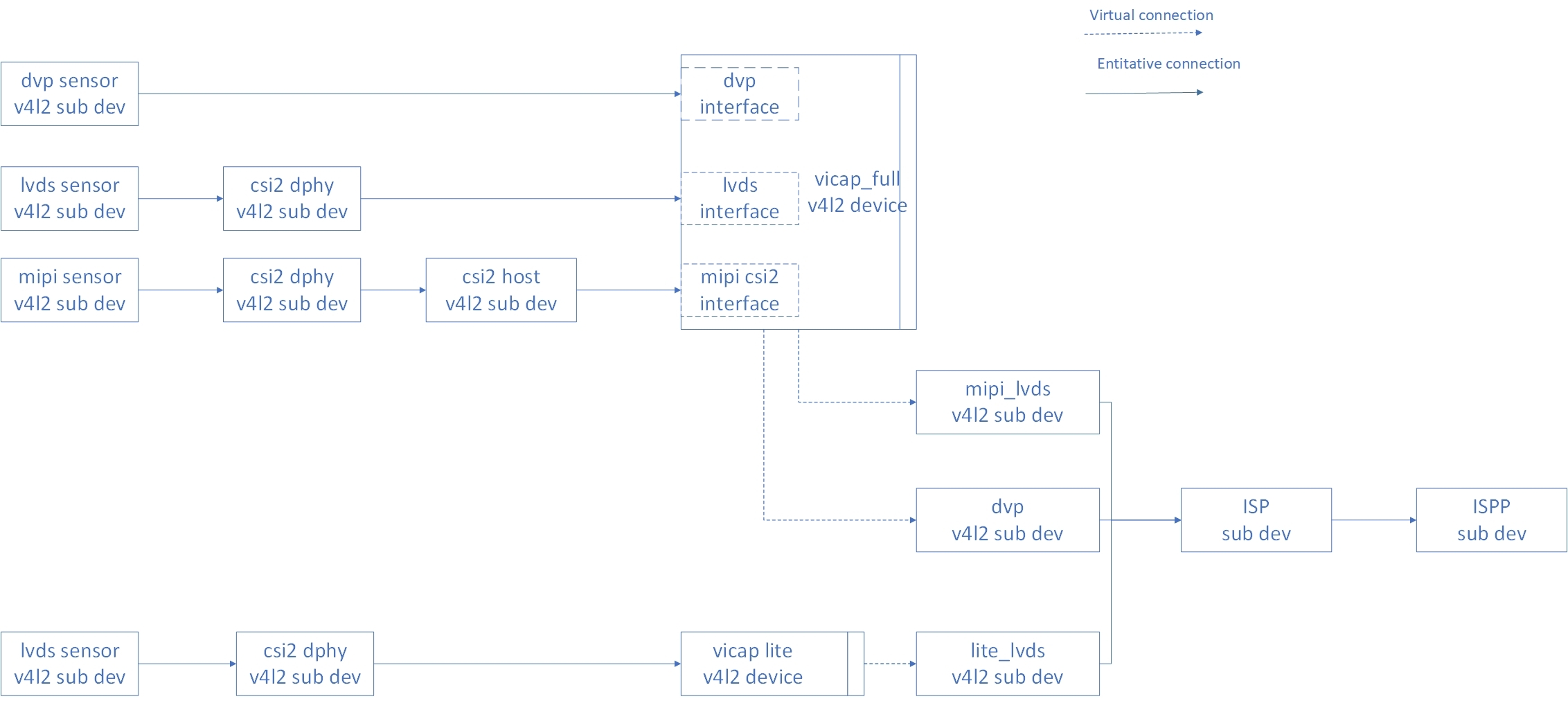
ISP and VICAP connection topology — original English figure, PDF page 10
4. RKISP driver
4.1 Brief description of the framework
The RKISP driver is mainly based on the v4l2/media framework to implement hardware configuration, interrupt processing, control buffer rotation, and control the power on and off of subdevices (such as MIPI DPHY and sensor).
The following block diagram describes the topology of the RKISP driver:
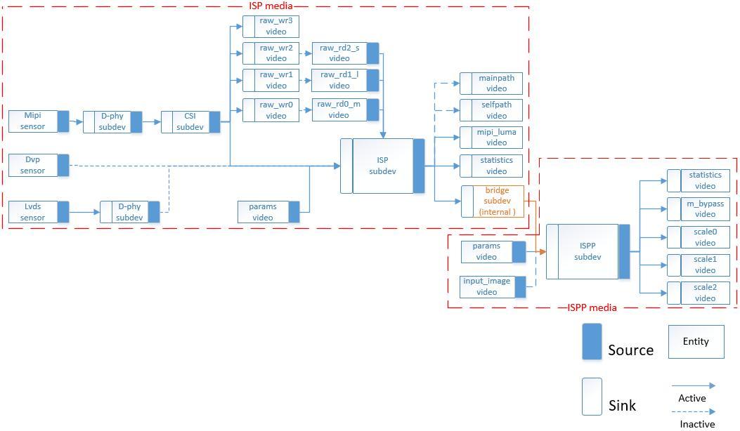
RKISP driver topology — original English figure, PDF page 11
| Name | Type | Description |
|---|---|---|
| rkisp_mainpath | v4l2_vdevcapture | Format: YUV, RAW Bayer; Support: Crop,scale(no for raw) |
| rkisp_selfpath | v4l2_vdevcapture | Format: YUV, RGB; Support: Crop,scale(no for raw) |
| rkisp-isp-subdev | v4l2_subdev | Internal isp blocks; Support: source/sink pad crop. The format on sink pad equal to sensor input format, the size equal to sensor input size. The format on source pad should be equal to vdev output format if output format is raw bayer, otherwise it should be YUYV2X8. The size should be equal/less than sink pad size. |
| rkisp-mipi-luma | v42_vdevcapture | Provice raw image luma |
| rkisp-statistics | v4l2_vdevcapture | Provide Image color Statistics information. |
| rkisp-input-params | v4l2_vdevoutput | Accept params for AWB, BLC…… Image enhancement blocks. |
| rkisp_rawrd0_m | v4l2_vdevoutput | Raw image read from DDR to ISP, usually using for the HDR middle frame |
| rkisp_rawrd1_l | v4l2_vdevoutput | Raw image read from DDR to ISP, usually using for the HDR long frame |
| rkisp_rawrd2_s | v4l2_vdevoutput | Raw image read from DDR to ISP, usually using for the HDR short frame |
| rkisp-csi-subdev | v4l2_subdev | MIPI CSI configure |
| rkisp_rawwr0 | v4l2_vdevcapture | Raw image write to DDR from sensor, usually using for the HDR middle frame |
| rkisp_rawwr1 | v4l2_vdevcapture | Raw image write to DDRfrom sensor, usually using for the HDR long frame |
| rkisp_rawwr2 | v4l2_vdevcapture | Raw image write to DDR from sensor, usually using for the HDR short frame |
| rkisp_rawwr3 | v4l2_vdevcapture | Raw image write to DDR from sensor |
| rockchip-mipi- dphy-rx | v4l2_subdev | MIPI-DPHY Configure. |
| rkisp-bridge-ispp | v4l2_subdev | ISP output yuv image to ISPP |
| rkispp_input_image | v4l2_vdevoutput | Yuv image read from DDR to ISPP |
| rkisp-isp-subdev | v4l2_subdev | The format and size on sink pad equal to ISP output. The support max size is 4416x3312, min size is 66x258 |
| rkispp_m_bypass | v4l2_vdev capture | Full resolution and yuv format |
| Name | Type | Description |
|---|---|---|
| rkispp_scale0 | v4l2_vdev capture | Full or scale resolution and yuv format Scale range:[1 8] ratio 3264 max width for yuv422 2080 max width for yuv420 only for rv1126 |
| rkispp_scale1 | v4l2_vdev capture | Full or scale resolution and yuv format Scale range:[2 8] ratio 1280 max width only for rv1126 |
| rkispp_scale2 | v4l2_vdev capture | Full or scale resolution and yuv format Scale range:[2 8] ratio 1280 max width only for rv1126 |
4.2 ISP HDR mode description
RKISP2 supports receiving MIPI sensor to output HDR 3 frames or 2 frames mode, the hardware collects data to DDR through 3 or 2 dmatx, and then reads the ISP through 3 or 2 dmarx, and the ISP does 3 or 2 frames synthesis, drive chain The road is as follows:
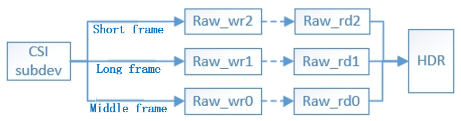
Three-frame HDR path — original English figure, PDF page 13
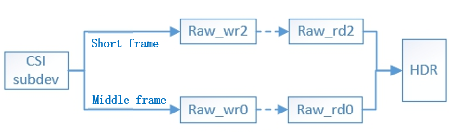
Two-frame HDR path — original English figure, PDF page 13
The CSI subdev obtains the output information of the sensor driver in multiple pad formats through get_fmt, which corresponds to the source pad of the CSI.
Please refer to the specific configuration of MIPI sensor driver Driver migration steps
| Name | Name | Description |
|---|---|---|
| rkisp-isp- subdev | Sensor pad0 | ISP capture Sensor vc0 (default) wide and high format output, commonly used linear mode |
| rkisp_rawwr0 | Sensor pad1 | Rawwr0 capture sensor vcX wide and high format output |
| rkisp_rawwr1 | Sensor pad2 | Rawwr1 capture sensor vcX wide and high format output |
| rkisp_rawwr2 | Sensor pad3 | Rawwr2 capture sensor vcX wide and high format output |
| rkisp_rawwr3 | Sensor pad4 | Rawwr3 capture sensor vcX wide and high format output |
5. RKVICAP driver
5.1 Frame description
The RKVICAP driver is mainly based on the v4l2/media framework to implement hardware configuration, interrupt processing, control buffer rotation, and control the power on and off of subdevices (such as mipi dphy and sensor).
For RV1126/RV1109, VICAP has two IP cores, one of which is called VICAP FULL and the other is called VICAP LITE. VICAP FULL has three interfaces: dvp/mipi/lvds, dvp can work with mipi or lvds interface at the same time, but mipi and lvds cannot work at the same time, VICAP LITE only has lvds interface, which can work with VICAP FULL interface at the same time; VICAP FULL dvp The interface corresponds to a rkvicap_dvp node, the VICAP FULL mipi/lvds interface corresponds to a rkvicap_mipi_lvds node, and the VICAP LITE corresponds to a rkvicap_lite_mipi_lvds node. Each node can be collected independently.
For the RK356X chip, VICAP has only a single core and has two interfaces, dvp and mipi. The dvp interface corresponds to a rkvicap_dvp node, and the mipi interface corresponds to a rkvicap_mipi_lvds node (the same name as the VICAP FULL of RV1126/RV1109), and each node can be collected independently.
In order to synchronize the data collected by VICAP to the isp driver, it is necessary to link the logical sditf node generated by the VICAP driver to the virtual node device generated by the isp. The DVP interface corresponds to the rkvicap_dvp_sditf node, the mipi/lvds interface of VICAP FULL corresponds to the rkvicap_mipi_lvds_sditf node, and the VICAP LITE corresponds to rkvicap_lite_sditf.
Please refer to the specific dts link method of each interface CIS Device Registration (DTS)
The following figure describes the topology of the device driven by RKVICAP:
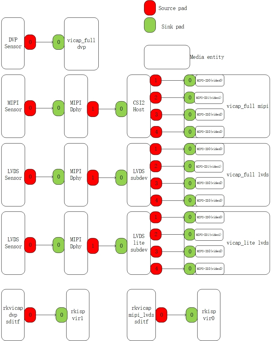
VICAP interface topology — original English figure, PDF page 15
6. RK3588 VI structure
7. Hardware Block
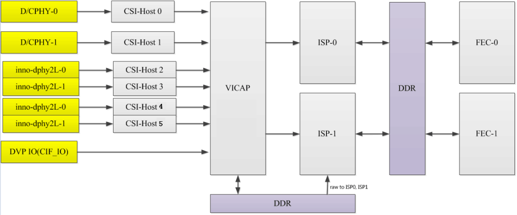
RK3588 VI hardware blocks — original English figure, PDF page 16
7.1 Multi-sensor support
A single hardware ISP supports up to four multiplexes, and the supported resolutions for ISP multiplexing are as follows:
2-way multiplexing: The maximum resolution is 3840x2160, and DTS corresponds to the configuration of 2-way rkisp_vir devices.
3-way or 4-way multiplexing: The maximum resolution is 2560x1536, and DTS corresponds to the configuration of 3 or 4-way rkisp_vir devices.
The hardware supports the acquisition of up to 7 sensors: 6MIPI + 1DVP, and the multi-sensor software path is as follows:
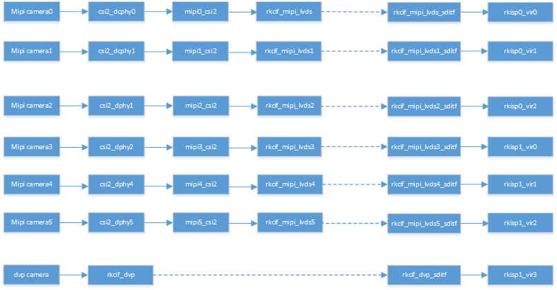
RK3588 multi-sensor paths — original English figure, PDF page 16
Block diagram description:
1. The RK3588 supports two DCPHYs with node names of csi2_dcphy0/csi2_dcphy1. Each dcphy hardware supports RX/TX at the same time, and RX is used for camera inputs. Support DPHY/CPHY protocol multiplexing; It should be noted that TX/RX of the same dcphy can only use DPHY at the same time or CPHY at the same time. Other DCPHY parameters can be found in the RK3588 data sheet. 2. RK3588 supports 2 DPY hardware, here we call it dphy0_hw/dphy1_hw, both DPHY hardware can work in Full Mode and Split Mode modes. 1. dphy0_hw 1. Full Mode: The node name is csi2_dphy0, and up to 4 lanes are supported. 2. Split Mode: Split into 2 PHYs, which are csi2_dphy1 (using 0/1 lane) and csi2_dphy2 (using 2/3 LANE), each PHY supports up to 2 lanes. 3. When dphy0_hw uses full mode, the link needs to be configured according to the csi2_dphy1 link, but the node name csi2_dphy1 needs to be modified to csi2_dphy0, and the software is distinguished by the sequence number of PHY to distinguish the mode used by PHY. 2. dphy1_hw 1. Full Mode: The node name uses csi2_dphy3, and supports up to 4 lanes. 2. Split Mode: Split into 2 PHYs, which are csi2_dphy4 (using 0/1 lane) and csi2_dphy5 (using 2/3 LANE), each PHY supports up to 2 lanes. 3. When dphy1_hw uses full mode, the link needs to be configured according to the csi2_dphy4 link, but the node name csi2_dphy4 need to be modified to csi2_dphy3, and the software is to distinguish the mode used by the PHY sequence number. 3. To use the above MIPI PHY node, you need to configure the corresponding physical node. (csi2_dcphy0_hw/csi2_dcphy1_hw/csi2_dphy0_hw/csi2_dphy1_hw) 4. Each MIPI PHY requires a CSI2 module to parse the MIPI protocol, and the node names are mipi0_csi2~mipi5_csi2. 5. All camera data in RK3588 needs to be linked to the ISP through ViCap. RK3588 only supports one VICAP hardware, this VICAP supports simultaneous input of 6 MIPI PHYs, and one DVP data, so we divide VICAP into 7 nodes such as rkcif_mipi_lvds~rkcif_mipi_lvds5, rkcif_dvp, etc., and the binding relationship of each node needs to be configured in strict accordance with the node serial number of the block diagram. 6. The link relationship between each VICAP node and the ISP indicates the link relationship by corresponding to the virtual XXX_sditf. 7. The RK3588 supports 2 ISP hardware, each ISP device can virtualize multiple virtual nodes, and the software reads each image data from the DDR in turn into the ISP for processing. For multi-camera scenarios, it is recommended to distribute the data stream evenly between the two ISPs. 8. Pass-through and readback modes: 1. Pass-through: means that the data is collected by VICAP, sent directly to the ISP for processing, and is not stored in DDR. It should be noted that when HDR pass-through, only short frames are true pass-through, long frames need to exist DDR, and ISP reads from DDR. 2. Read back: It means that the data is collected to the DDR through VICAP, and after the application obtains the data, it pushes the buffer address to the ISP, and the ISP obtains the image data from the DDR. 3. When configuring DTS again, if only one virtual node is configured, passthrough mode is used by default for an ISP hardware, and readback mode is used by default if multiple virtual nodes are configured.
7.2 Dual ISP synthesis supports 8K resolution
VICAP collects sensor 8K data, then sends the left and right images to two ISPs for processing, and then outputs them to DDR, the process is as follows:
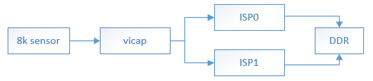
Dual-ISP 8K synthesis — original English figure, PDF page 18
When the resolution is greater than 16M (4672x3504), two ISPs need to be used at the same time to process one image, and only single camera is supported.
1. From the rk3588s.dtsi file, you can find the three definitions of rkisp0, rkisp1, and rkisp_unite, when the resolution to be processed is greater than 16M, you need to close the rkisp0 and rkisp1 nodes, and enable the rkisp_unite, while modifying the corresponding iommu node.
2. Using rkisp_unite nodes can also virtualize multiple nodes, at this time, regardless of the resolution, the same image is cropped into two pictures, left and right, sent 2 ISPs for processing, and then synthesized into an output.
3. DTS Configuration Reference 待链接
7.3 8 mesh MIPI sensor support
RK3588 hardware supports up to 6 mipi sensors, which can be expanded by RK1608 splicing, RK1608 supports 4 MIPI inputs (1, 2, 4lane), two MIPI outputs (1, 2, 4lane), through RK1608 splicing 3 + original 5 MIPI can achieve 8 MIPI sensor inputs, the hardware connection is as follows:
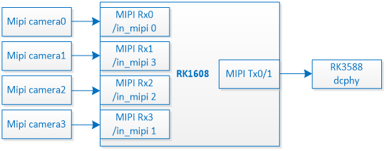
RK1608 eight-MIPI-sensor connection — original English figure, PDF page 18
Software, you need to enable the RK1608 driver in the kernel’s defconfig:
  CONFIG_VIDEO_ROCKCHIP_PREISP=y
  CONFIG_VIDEO_PREISP_DUMMY_SENSOR=y
On the dts link, RK1608 abstracts the RK1608 dphy node and enters it as a virtual preisp_dmy sensor. RK1608 dphy, like ordinary sensors, is connected to RK3588 dcphy to form an RK1608->dcphy->csi->cif lvds link. The sensor physically hung in the RK1608 is directly hung in the rkcif_mipi_lvdsx_sditf, rkcif_mipi_lvdsx_sditf_vir1, rkcif_mipi_lvdsx_sditf_vir2, and rkcif_mipi_lvdsx_sditf_vir3 port0 in the dts as the input of the SDITF device.
The output of SDITF is consistent with the original path, and is the corresponding ISP node. The DTS link is shown as follows:
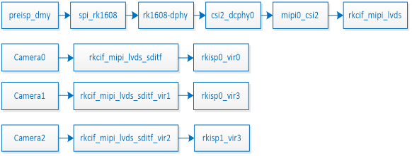
RK1608 DTS link topology — original English figure, PDF page 19
The dts configuration of RK1608 is mainly on the rk1608-dpy device node, which mainly includes input and output channels and resolution, as follows:
  #define LINK_FREQ               700000000
      mipidphy0: mipidphy0 {
      compatible =  "rockchip,rk1608-dphy";
          status = "okay";
          //rockchip,grf = <&grf>;
          id = <0>;  //RK1608 internal ID (0-2, spliced sequentially by ID)
          cam_nums = <1>;
          in_mipi = <1>;         //Input MIPI channel of the first sensor (0-3)
          out_mipi = <0>;        //Output MIPI channel (0-1)
          link-freqs = /bits/ 64 <LINK_FREQ>; //MIPI rate
          sensor_i2c_bus = <5>;     //The 8-mesh pattern is invalid
          sensor_i2c_addr = <0x1a>; //The 8-mesh pattern is invalid
          sensor-name = "IMX464";
          rockchip,camera-module-index = <9>; //Same as ordinary sensor
          rockchip,camera-module-facing = "back";
          rockchip,camera-module-name = "TongJu";
          rockchip,camera-module-lens-name = "CHT842-MD";
          /* virtual-sensor mode */
          virtual-sub-sensor-config-0 {  //Configuration information for the second
  sensor
              id = <1>;  //RK1608 internal ID (0-2, spliced by ID)
              in_mipi = <2>;
              out_mipi = <1>;
          };
          virtual-sub-sensor-config-1 { //Configuration information for the third
  sensor
              id = <2>;  //RK1608 internal ID (0-2, spliced by ID)
              in_mipi = <3>;
              out_mipi = <1>;
          };
          /* multi-sensor mode end */
          format-config-0 {
              data_type = <0x2b>;
              mipi_lane = <2>;     //The number of lanes connected to the sensor
              mipi_lane_out = <4>; //The number of lanes output by RK1608
              field = <1>;      //The following is the same as the normal sensor
  configuration
              colorspace = <8>;
              code = <MEDIA_BUS_FMT_SRGGB10_1X10>;
              width = <2712>;  //Sensor output resolution
              height= <1538>;
              hactive = <2712>; //RK1608 output resolution, the same width, height
  is n*sensor
              vactive = <4614>;
              htotal = <3616>; //After increasing the width and height of blank,
  30% of the blank is generally required
              vtotal = <4710>;
              inch0-info = <2712 1538 0x2b 0x2b 1>; //Sensor output resolution
              outch0-info = <2712 4614 0x2b 0x2b 1>; //RK1608 output resolution
              hcrop = <2560>; //Single resolution after cropping
              vcrop = <1520>;
          };
          ...
The DTS configuration reference of the sensor is as follows:
  &rkcif_mipi_lvds_sditf {
      #address-cells = <1>;
      #size-cells = <0>;
      status = "okay";
      rockchip,combine-index = <0>; //Order in RK1608 stitching diagram
      ports {
          #address-cells = <1>;
          #size-cells = <0>;
          port@0 {
              reg = <0>;
              #address-cells = <1>;
              #size-cells = <0>;
              mipi_lvds_sditf_in: endpoint@1 {
                  reg = <1>;
                  remote-endpoint = <&imx464_out7>;
                  data-lanes = <1 2>;
              };
          };
          port@1 {
              reg = <1>;
              #address-cells = <1>;
              #size-cells = <0>;
              mipi_lvds_sditf: endpoint@0 {
                  reg = <0>;
                  remote-endpoint = <&isp0_vir0>;
              };
          };
      };
  };
8. CIS (CMOS image sensor) driver
8.1 CIS Device Registration (DTS)
8.1.1 MIPI interface
For the RV1126 and RV1106 platforms, there are two separate and complete standard physical MIPI CSI2 DPYs, corresponding to the csi_dphy0 and csi_dphy1 on the DTS (see RV1126.DTSI), with the following characteristics:
Data lanes are up to 4 lanes;
Maximum speed 2.5Gbps/lane;
For the RK356X platform, there is only one standard physical mipi csi2 dphy, which can operate in two modes: full mode and split mode, split into three logical dphys csi2_dphy0/csi2_dphy1/csi2_dphy2 (see rk3568.dtsi), with the following characteristics:
Full mode
Only use csi2_dphy0, csi2_dphy0 and csi2_dphy1/csi2_dphy2 mutually exclusive, not at the same time;
Data lanes up to 4 lanes;
Maximum speed 2.5Gbps/lane;
Split mode
Use only csi2_dphy1 and csi2_dphy2, mutually exclusive with csi2_dphy0, not at the same time;
csi2_dphy1 and csi2_dphy2 can be used at the same time;
The maximum data lanes of csi2_dphy1 and csi2_dphy2 are 2 lanes;
csi2_dphy1 lane0/lane1 corresponding to physical DPY;
csi2_dphy2 Lane2/LANE3 corresponding to physical DPY;
Maximum rate 2.5Gbps/lane
For specific DTS use cases, see the following examples.
8.1.1.1 Link ISP
8.1.1.1.1 RV1126/RV1106
The following is an example of RV1126 ISP and OS04A10.
Link relationship: sensor->csi_dphy->isp->ispp
arch/arm/boot/dts/rv1126-evb-v10.dtsi
Configuration Essentials
Data-lanes must indicate the specific number of lanes used, otherwise they cannot be recognized as mipi types;
  cam_ircut0: cam_ircut {
      status = "okay";
      compatible = "rockchip,ircut";
      ircut-open-gpios = <&gpio2 RK_PA7 GPIO_ACTIVE_HIGH>;
      ircut-close-gpios = <&gpio2 RK_PA6 GPIO_ACTIVE_HIGH>;
      rockchip,camera-module-index = <1>;
      rockchip,camera-module-facing = "front";
  };
  os04a10: os04a10@36 {
      compatible = "ovti,os04a10";// It needs to match the matching string in the
  driver
      reg = <0x36>;// sensor I2C device address, 7 bits
      clocks = <&cru CLK_MIPICSI_OUT>;// Sensor clickin configuration
      clock-names = "xvclk";
      power-domains = <&power RV1126_PD_VI>;
      pinctrl-names = "rockchip,camera_default";
      pinctrl-0 = <&mipi_csi_clk0>;// PINCTL settings
      //power supply
      avdd-supply = <&vcc_avdd>;
      dovdd-supply = <&vcc_dovdd>;
      dvdd-supply = <&vcc_dvdd>;
      // Power pin assignment and active level
      pwdn-gpios = <&gpio1 RK_PD4 GPIO_ACTIVE_HIGH>;
      // Module number, which should not be repeated
      rockchip,camera-module-index = <1>;
      // Module orientation, with "back" and "front"
      rockchip,camera-module-facing = "front";
      // Module name
      rockchip,camera-module-name = "CMK-OT1607-FV1";
      // Lens name
      rockchip,camera-module-lens-name = "M12-4IR-4MP-F16";
      //IR CUT equipment
      ir-cut = <&cam_ircut0>;
      port {
          ucam_out0: endpoint {
              // The port name on the mipi dphy side
              remote-endpoint = <&mipi_in_ucam0>;
              // MIPI lanes number, 1 lane is <1>,
              4lane is <1 2 3 4 >
              data-lanes = <1 2 3 4>;
          };
      };
   };
  &csi_dphy0 {
      status = "okay";
      ports {
          #address-cells = <1>;
          #size-cells = <0>;
          port@0 {
              reg = <0>;
              #address-cells = <1>;
              #size-cells = <0>;
              mipi_in_ucam0: endpoint@1 {
                  reg = <1>;
                  // The port name on the sensor side
                  remote-endpoint = <&ucam_out0>;
                  // MIPI lanes number, 1 lane is <1>, 4lane is
  <1 2 3 4 >,data-lanes = <1 2 3 4>;
              };
          };
          port@1 {
              reg = <1>;
              #address-cells = <1>;
              #size-cells = <0>;
              csidphy0_out: endpoint@0 {
                  reg = <0>;
                  // The port name on the ISP side
                  remote-endpoint = <&isp_in>;
              };
          };
      };
  };
  &rkisp {
      status = "okay";
  };
  &rkisp_vir0 {
      status = "okay";
      ports {
          #address-cells = <1>;
          #size-cells = <0>;
          port@0 {
              reg = <0>;
              #address-cells = <1>;
              #size-cells = <0>;
              isp_in: endpoint@0 {
                  reg = <0>;
                  // The port name on the mipi dphy side
                  remote-endpoint = <&csidphy0_out>;
              };
          };
          port@1 {
              reg = <1>;
              #address-cells = <1>;
              #size-cells = <0>;
              isp0_out: endpoint@1 {
                  reg = <1>;
                  // ISP port name, ISP output to ISP
                  remote-endpoint = <&ispp0_in>;
              };
          };
      };
  };
  &rkispp {
      status = "okay";
  };
  &rkispp_vir0 {
      status = "okay";
      port {
          #address-cells = <1>;
          #size-cells = <0>;
          Ispp0_in: endpoint@0 {
              reg = <0>;
              // ISP port name, ISPP input
              remote-endpoint = <&isp0_out>;
          };
      };
  };
8.1.1.1.2 RK356X
The following is an example of RK3566 ISP and GC8034 4LANE:
Link relationship: sensor->csi2_dphy0->isp Configuration Essentials
Data-lanes need to be configured
Requires csi2_dphy_hw node to be enabled
   /* full mode: lane0-3 */
      gc8034: gc8034@37 {
          // It needs to match the matching string in the driver
          compatible = "galaxycore,gc8034";
          status = "okay";
          // sensor I2C device address, 7 bits
          reg = <0x37>;
          // Sensor mclk source configuration
          clocks = <&cru CLK_CIF_OUT>;
          clock-names = "xvclk";
          //The sensor dependent power domain is enabled
          power-domains = <&power RK3568_PD_VI>;
          //Sensor McLk pinctl settings
          pinctrl-names = "default";
          pinctrl-0 = <&cif_clk>;
          // Reset pin assignment and active level
          reset-gpios = <&gpio3 RK_PA6 GPIO_ACTIVE_LOW>;
          // Powerdown pin assignment and active level
          pwdn-gpios = <&gpio4 RK_PB2 GPIO_ACTIVE_LOW>;
          // Module number, which should not be repeated
          rockchip,camera-module-index = <0>;
          // Module orientation, with "back" and "front"
          rockchip,camera-module-facing = "back";
          // Module name
          rockchip,camera-module-name = "RK-CMK-8M-2-v1";
          // Lens name
          rockchip,camera-module-lens-name = "CK8401";
          port {
              gc8034_out: endpoint {
                  // The port name of the CSI2 dphy end
                  remote-endpoint = <&dphy0_in>;
                  // CSI2 dphy lane number, 1lane is <1>,
                  4lane is <1 2 3 4>, data-lanes = <1 2 3 4>;
              };
          };
      };
      &csi2_dphy_hw {
         status = "okay";
      };
      &csi2_dphy0 {
          //csi2_dphy0 is not used at the same time as
          csi2_dphy1/csi2_dphy2, mutually exclusive
          status = "okay";
          /*
           * dphy0 only used for full mode,
           * full mode and split mode are mutually exclusive
           */
          ports {
              #address-cells = <1>;
              #size-cells = <0>;
              port@0 {
                  reg = <0>;
                  #address-cells = <1>;
                  #size-cells = <0>;
                  dphy0_in: endpoint@1 {
                      reg = <1>;
                      // The port name on the sensor side
                      remote-endpoint = <&gc8034_out>;
                      // CSI2 dphy lanes, 1 lane is <1 >, 4 lanes is <1 2 3 4 >,
  which needs to be consistent with the sensor side
                          data-lanes = <1 2 3 4>;
                  };
              };
              port@1 {
                  reg = <1>;
                  #address-cells = <1>;
                  #size-cells = <0>;
                  dphy0_out: endpoint@1 {
                      reg = <1>;
                      // The port name on the ISP side
                      remote-endpoint = <&isp0_in>;
                  };
              };
          };
      };
  &rkisp {
      status = "okay";
  };
  &rkisp_mmu {
      status = "okay";
  };
  &rkisp_vir0 {
      status = "okay";
      port {
          #address-cells = <1>;
          #size-cells = <0>;
          isp0_in: endpoint@0 {
              reg = <0>;
              // The port name of the CSI2 dphy side
              remote-endpoint = <&dphy0_out>;
          };
      };
  };
8.1.1.2 Link VICAP
8.1.1.2.1 RV1126/RV1109
Take MIPI OS04A10 4 Lanes Link VICAP as an example:
Link relationship: sensor->csi dphy->mipi csi host->vicap Configuration Points:
Data-lanes must indicate the specific number of lanes used, otherwise they cannot be recognized as MIPI types;
dphy needs to be linked to the CSI Host node.
  os04a10: os04a10@36 {
          // It needs to match the matching string in the driver
          compatible = "ovti,os04a10";
          // sensor I2C device address, 7 bits
          reg = <0x36>;
          // Sensor mclk source configuration
          clocks = <&cru CLK_MIPICSI_OUT>;
          clock-names = "xvclk";
          //The sensor dependent power domain is enabled
          power-domains = <&power RV1126_PD_VI>;
          avdd-supply = <&vcc_avdd>;
          dovdd-supply = <&vcc_dovdd>;
          dvdd-supply = <&vcc_dvdd>;
          //Sensor McLk pinctl settings
          pinctrl-names = "rockchip,camera_default";
          pinctrl-0 = <&mipicsi_clk0>;
          // Powerdown pin assignment and active level
          pwdn-gpios = <&gpio1 RK_PD4 GPIO_ACTIVE_HIGH>;
          // Module number, which should not be repeated
          rockchip,camera-module-index = <1>;
          // Module orientation, with "back" and "front"
          rockchip,camera-module-facing = "front";
          // Module name
          rockchip,camera-module-name = "CMK-OT1607-FV1";
          // Lens name
          rockchip,camera-module-lens-name = "M12-40IRC-4MP-F16";
          // Ircut name
          ir-cut = <&cam_ircut0>;
          port {
              ucam_out0: endpoint {
                  // The port name of the CSI2 dphy end
                  remote-endpoint = <&mipi_in_ucam0>;
                  // CSI2 dphy lanes number, 1lane is <1>, 4lane is <1 2 3 4 >
                  data-lanes = <1 2 3 4>;
              };
          };
      };
  &csi_dphy0 {
      //csi2_dphy0 is not used at the same time as csi2_dphy1/csi2_dphy2, mutually exclusive
      status = "okay";
      ports {
          #address-cells = <1>;
          #size-cells = <0>;
          port@0 {
              reg = <0>;
              #address-cells = <1>;
              #size-cells = <0>;
              mipi_in_ucam0: endpoint@1 {
                  reg = <1>;
                  // The port name on the sensor side
                  remote-endpoint = <&ucam_out0>;
                  // CSI2 dphy lanes, 1 lane is <1 >, 4 lanes is <1 2 3 4 >, which
  needs to be consistent with the sensor side
                  data-lanes = <1 2 3 4>;
              };
          };
          port@1 {
              reg = <1>;
              #address-cells = <1>;
              #size-cells = <0>;
              csidphy0_out: endpoint@0 {
                  reg = <0>;
                  // The port name of the CSI2 host
                  remote-endpoint = <&mipi_csi2_input>;
              };
          };
      };
  };
  &mipi_csi2 {
      status = "okay";
      ports {
          #address-cells = <1>;
          #size-cells = <0>;
          port@0 {
              reg = <0>;
              #address-cells = <1>;
              #size-cells = <0>;
              mipi_csi2_input: endpoint@1 {
                  reg = <1>;
                  // The port name of the CSI2 host
                  remote-endpoint = <&csidphy0_out>;
                  // CSI2 host lanes, 1 lane is <1>,
                  4lane is <1 2 3 4 >, which needs to be
                  consistent with the sensor side
                  data-lanes = <1 2 3 4>;
              };
          };
          port@1 {
              reg = <1>;
              #address-cells = <1>;
              #size-cells = <0>;
              mipi_csi2_output: endpoint@0 {
                  reg = <0>;
                  // The port name on the vicap side
                  remote-endpoint = <&cif_mipi_in>;
                  // CSI2 host lanes, 1 lane is <1>,
                  4lane is <1 2 3 4 >, which needs to be
                  consistent with the sensor side
                  data-lanes = <1 2 3 4>;
              };
          };
      };
  };
  &rkcif_mipi_lvds {
      status = "okay";
      port {
          /* MIPI CSI-2 endpoint */
          cif_mipi_in: endpoint {
              // The port name of the CSI2 host
              remote-endpoint = <&mipi_csi2_output>;
              // The number of lanes on the vicap side,
              1 lane is <1 >, 4lane is < 1 2 3 4 >,
              which needs to be consistent with the sensor side
              data-lanes = <1 2 3 4>;
          };
      };
  };
  &rkcif_mipi_lvds_sditf {
      status = "okay";
      port {
          /* sditf endpoint */
          mipi_lvds_sditf: endpoint {
              //ISP virtual device port name
              remote-endpoint = <&isp_in>;
              //The number of lanes of MIPI CSI2 dphy,
              consistent with the sensor
              data-lanes = <1 2 3 4>;
          };
      };
  };
  &rkisp {
      status = "okay";
  };
  &rkisp_vir0 {
      status = "okay";
      ports {
          port@0 {
              reg = <0>;
              #address-cells = <1>;
              #size-cells = <0>;
              isp_in: endpoint@0 {
                  reg = <0>;
                  //The endpoint name of the Vicap SDITF
                  remote-endpoint = <&mipi_lvds_sditf>;
              };
          };
      };
  };
8.1.1.2.2 RK356X
Take the example of lane2/lane3 of GC5025 2lane link rk3566 EVB2 mipi CSI2 dphy:
Link relationship: sensor->csi2 dphy->mipi CSI host->vicap Configuration Essentials
Data-lanes must indicate the specific number of lanes used, otherwise they cannot be recognized as MIPI types;
dphy needs to be linked to the CSI Host node;
The CSI2 dphy HW node needs to be enabled.
  /* split mode: lane:2/3 */
  gc5025: gc5025@37 {
          status = "okay";
          // It needs to match the matching string in the driver
          compatible = "galaxycore,gc5025";
          // sensor I2C device address, 7 bits
          reg = <0x37>;
          // Sensor mclk source configuration
          clocks = <&pmucru CLK_WIFI>;
          clock-names = "xvclk";
          //Sensor McLk pinctl settings
          pinctrl-names = "default";
          pinctrl-0 = <&refclk_pins>;
          // Reset pin assignment and active level
          reset-gpios = <&gpio3 RK_PA5 GPIO_ACTIVE_LOW>;
          // Powerdown pin assignment and active level
          pwdn-gpios = <&gpio3 RK_PB0 GPIO_ACTIVE_LOW>;
          // The sensor dependent power domain is enabled
          power-domains = <&power RK3568_PD_VI>;
          /*power-gpios = <&gpio0 RK_PC1 GPIO_ACTIVE_HIGH>;*/
          // Module number, which should not be repeated
          rockchip,camera-module-index = <1>;
          // Module orientation, with "back" and "front"
          rockchip,camera-module-facing = "front";
          // Module name
          rockchip,camera-module-name = "TongJu";
          // Lens name
          rockchip,camera-module-lens-name = "CHT842-MD";
          port {
              gc5025_out: endpoint {
                  // The port name of the CSI2 dphy end
                  remote-endpoint = <&dphy2_in>;
                  // CSI2 dphy lanes number, 2lanes are <1 2>, 4lanes are <1 2 3 4
  >
                  data-lanes = <1 2>;
              };
          };
  };
   &csi2_dphy_hw {
           status = "okay";
   };
  &csi2_dphy2 {
      //csi2_dphy2 is not used at the same time as csi2_dphy0, mutually exclusive;
  Can be used in parallel with csi2_dphy1
      status = "okay";
      /*
       * dphy2 only used for split mode,
       * can be used  concurrently  with dphy1
       * full mode and split mode are mutually exclusive
       */
      ports {
          #address-cells = <1>;
          #size-cells = <0>;
          port@0 {
              reg = <0>;
              #address-cells = <1>;
              #size-cells = <0>;
              dphy2_in: endpoint@1 {
                  reg = <1>;
                  // The port name on the sensor side
                  remote-endpoint = <&gc5025_out>;
                  // CSI2 dphy lanes, 2lane is <1 2>, 4lane is <1 2 3 4 >, which
  needs to be consistent with the sensor side
                  data-lanes = <1 2>;
              };
          };
          port@1 {
              reg = <1>;
              #address-cells = <1>;
              #size-cells = <0>;
              dphy2_out: endpoint@1 {
                  reg = <1>;
                  // The port name of the CSI2 host
                  remote-endpoint = <&mipi_csi2_input>;
              };
          };
      };
  };
  &mipi_csi2 {
      status = "okay";
      ports {
          #address-cells = <1>;
          #size-cells = <0>;
          port@0 {
              reg = <0>;
              #address-cells = <1>;
              #size-cells = <0>;
              mipi_csi2_input: endpoint@1 {
                  reg = <1>;
                  // The port name on the CSI2 dphy side
                  remote-endpoint = <&dphy2_out>;
                  // CSI2 host lanes, 2 lanes are <1 2>, 4lanes are <1 2 3 4 >,
  which need to be consistent with the sensor side
                  data-lanes = <1 2>;
              };
          };
          port@1 {
              reg = <1>;
              #address-cells = <1>;
              #size-cells = <0>;
              mipi_csi2_output: endpoint@0 {
                  reg = <0>;
                  // The port name on the vicap side
                  remote-endpoint = <&cif_mipi_in>;
                  // CSI2 host lanes, 1 lane is <1>, 4lane is <1 2 3 4 >, which
  needs to be consistent with the sensor side
                  data-lanes = <1 2>;
              };
          };
      };
  };
  &rkcif_mipi_lvds {
      status = "okay";
      port {
          cif_mipi_in: endpoint {
              // The port name of the CSI2 host
              remote-endpoint = <&mipi_csi2_output>;
              // The number of lanes on the vicap side, 2lane is <1 2>, 4lane is <1
  2 3 4 >, which needs to be consistent with the sensor side
              data-lanes = <1 2>;
          };
      };
  };
  &rkcif_mipi_lvds_sditf {
      status = "okay";
      port {
          /* MIPI CSI-2 endpoint */
          mipi_lvds_sditf: endpoint {
              //ISP virtual device port name
              remote-endpoint = <&isp_in>;
              //The number of lanes of MIPI CSI2 dphy, consistent with the sensor
              data-lanes = <1 2>;
          };
      };
  };
  &rkisp {
      status = "okay";
  };
  &rkisp_vir0 {
      status = "okay";
      ports {
          port@0 {
              reg = <0>;
              #address-cells = <1>;
              #size-cells = <0>;
              isp_in: endpoint@0 {
                  reg = <0>;
                  //The endpoint name of Vicap Mipi SDITF
                  remote-endpoint = <&mipi_lvds_sditf>;
              };
          };
      };
  };
8.1.1.2.3 RK3588
Take IMX464 connected to DPY1 as an example
Data-lanes must indicate the specific number of lanes used, otherwise they cannot be recognized as mipi types;
dphy needs to be linked to the CSI Host node, csi2_dphy3 corresponds to the mipi4_csi2 used;
csi2_dphy3 are just logical nodes and need to rely on physical nodes csi2_dphy1_hw.
rkcif_mipi_lvds4 is one of the logical nodes of vicap, and the physical node rkcif and corresponding iommu need to be configured.
rkcif_mipi_lvds4_sditf is a virtual child node, which is a rkcif_mipi_lvds4 virtual node that is used to link ISPs.
The sensor driver generally realizes AVDD/DVDD/DOVDD three power supply operation, if the power supply similar to the RAK809 allocated can be directly configured on the sensor node, if the LDO and other external power supplies, the enabling pin is controlled by GPIO, you can refer to the vcc_mipicsi1 configured as a power node, can be powered up and down by reference counting, suitable for multiple devices using the same power supply. It is recommended that the DVD power supply is supplied separately when multi-camera, AVDD/DOVDD can be shared, and when the DVD is shared, if the power is relatively large, there may be an instantaneous shortage of supply, and the power supply will collapse, affecting the image quality, or even not drawing.
      / {
          vcc_mipicsi1: vcc-mipicsi1-regulator {
              compatible = "regulator-fixed";
              gpio = <&gpio4 RK_PA6 GPIO_ACTIVE_HIGH>;
              pinctrl-names = "default";
              pinctrl-0 = <&mipicsi1_pwr>;
              regulator-name = "vcc_mipicsi1";
              enable-active-high;
          };
      };
      &csi2_dphy1_hw {
          status = "okay";
      };
      &csi2_dphy3 {
          status = "okay";
          ports {
              #address-cells = <1>;
              #size-cells = <0>;
              port@0 {
                  reg = <0>;
                  #address-cells = <1>;
                  #size-cells = <0>;
                  mipi_in_ucam: endpoint@1 {
                      reg = <1>;
                      remote-endpoint = <&imx464_out>;
                      data-lanes = <1 2 3 4>;
                  };
              };
              port@1 {
                  reg = <1>;
                  #address-cells = <1>;
                  #size-cells = <0>;
                  csidphy3_out: endpoint@0 {
                      reg = <0>;
                      remote-endpoint = <&mipi4_csi2_input>;
                  };
              };
          };
      };
      &i2c4 {
          status = "okay";
          pinctrl-0 = <&i2c4m3_xfer>;
          imx464: imx464@36 {
              compatible = "sony,imx464";
              status = "okay";
              reg = <0x36>;
              clocks = <&cru CLK_MIPI_CAMARAOUT_M4>;
              clock-names = "xvclk";
              pinctrl-names = "default";
              pinctrl-0 = <&mipim0_camera4_clk>;
              avdd-supply = <&vcc_mipicsi1>;
              reset-gpios = <&gpio1 RK_PD6 GPIO_ACTIVE_HIGH>;
              pwdn-gpios = <&gpio3 RK_PC1 GPIO_ACTIVE_HIGH>;
              rockchip,camera-module-index = <0>;
              rockchip,camera-module-facing = "back";
              rockchip,camera-module-name = "CMK-OT1980-PX1";
              rockchip,camera-module-lens-name = "SHG102";
              port {
                  imx464_out: endpoint {
                      remote-endpoint = <&mipi_in_ucam>;
                      data-lanes = <1 2 3 4>;
                  };
              };
          };
      };
      &mipi4_csi2 {
          status = "okay";
          ports {
              #address-cells = <1>;
              #size-cells = <0>;
              port@0 {
                  reg = <0>;
                  #address-cells = <1>;
                  #size-cells = <0>;
                  mipi4_csi2_input: endpoint@1 {
                      reg = <1>;
                      remote-endpoint = <&csidphy3_out>;
                  };
              };
              port@1 {
                  reg = <1>;
                  #address-cells = <1>;
                  #size-cells = <0>;
                  mipi4_csi2_output: endpoint@0 {
                      reg = <0>;
                      remote-endpoint = <&cif_mipi_in4>;
                  };
              };
          };
      };
      &pinctrl {
          cam {
              mipicsi1_pwr: mipicsi1-pwr {
                  rockchip,pins =
                      /* camera power en */
                      <4 RK_PA6 RK_FUNC_GPIO &pcfg_pull_none>;
              };
          };
      };
      &rkcif {
          status = "okay";
      };
      &rkcif_mipi_lvds4 {
          status = "okay";
          port {
              cif_mipi_in4: endpoint {
                  remote-endpoint = <&mipi4_csi2_output>;
              };
          };
      };
      &rkcif_mipi_lvds4_sditf {
          status = "okay";
          port {
              mipi4_lvds_sditf: endpoint {
                  remote-endpoint = <&isp0_vir0>;
              };
          };
      };
      &rkcif_mmu {
          status = "okay";
      };
      #if 1
      &rkisp0 {
          status = "okay";
          /* the max input w h and fps of mulit sensor */
          //max-input = <2688 1520 30>;多摄sensor分辨率不一样,需要配置
      };
      &isp0_mmu {
          status = "okay";
      };
      #else //sensor分辨率大于16M(4672x3504)需要2个isp合成处理
      /* dual isp case need width 32 align, height 8 align */
      &rkisp_unite_mmu {
          status = "okay";
      };
      &rkisp_unite {
             status = "okay";
      };
      &rkisp0_vir0 {
             status = "okay";
             rockchip,hw = <&rkisp_unite>;
      };
      #endif
      &rkisp0_vir0 {
          status = "okay";
          port {
              #address-cells = <1>;
              #size-cells = <0>;
              isp0_vir0: endpoint@0 {
                  reg = <0>;
                  remote-endpoint = <&mipi4_lvds_sditf>;
              };
          };
      };
8.1.1.2.4 RV1106
DTS configuration refer to arch/arm/boot/dts/rv1106-evb-cam.dtsi
8.1.1.2.5 ***RK3562
DTS configuration refer to arch/arm64/boot/dts/rockchip/rk3562-evb1-cam.dtsi
8.1.2 LVDS interface
8.1.2.1 Link VICAP
8.1.2.1.1 RV1126/RV1109
Taking IMX327 4lane as an example, the link relationship is as follows:
Link relationship: sensor->csi dphy->vicap Configuration Essentials
dphy does not need to link the CSI Host node, otherwise it will not receive data;
Data-lanes must indicate the specific number of lanes used, otherwise data will not be received;
bus-type must be configured as 3, otherwise it cannot be recognized as an LVDS interface, resulting in link establishment failure;
  imx327: imx327@1a {
          // It needs to match the matching string in the driver
          compatible = "sony,imx327";
          // sensor I2C device address, 7 bits
          reg = <0x1a>;
          // Sensor mclk source configuration
          clocks = <&cru CLK_MIPICSI_OUT>;
          clock-names = "xvclk";
          //The sensor dependent power domain is enabled
          power-domains = <&power RV1126_PD_VI>;
          avdd-supply = <&vcc_avdd>;
          dovdd-supply = <&vcc_dovdd>;
          dvdd-supply = <&vcc_dvdd>;
          //Sensor McLk pinctl settings
          pinctrl-names = "default";
          pinctrl-0 = <&mipicsi_clk0>;
          // Powerdown pin assignment and active level
          pwdn-gpios = <&gpio3 RK_PA6 GPIO_ACTIVE_HIGH>;
          // Reset pin assignment and active level
          reset-gpios = <&gpio1 RK_PD5 GPIO_ACTIVE_HIGH>;
          // Module number, which should not be repeated
          rockchip,camera-module-index = <1>;
          // Module orientation, with "back" and "front"
          rockchip,camera-module-facing = "front";
          // Module name
          rockchip,camera-module-name = "CMK-OT1607-FV1";
          // Lens name
          rockchip,camera-module-lens-name = "M12-4IR-4MP-F16";
          // Ircut name
          ir-cut = <&cam_ircut0>;
          port {
              ucam_out0: endpoint {
                  // The port name of the CSI2 dphy end
                  remote-endpoint = <&mipi_in_ucam0>;
                  //CSI2 dphy lvds number of lanes, 1 lane is <1>, 4lane is <4 >,
  must be specified
                  data-lanes = <4>;
                  //The type of LVDS interface, which must be specified
                  bus-type = <3>;
              };
          };
  };
  &csi_dphy0 {
      //csi2_dphy0 is not used at the same time as csi2_dphy1/csi2_dphy2, mutually exclusive
      status = "okay";
      ports {
          #address-cells = <1>;
          #size-cells = <0>;
          port@0 {
              reg = <0>;
              #address-cells = <1>;
              #size-cells = <0>;
              mipi_in_ucam0: endpoint@1 {
                  reg = <1>;
                  // The port name on the sensor side
                  remote-endpoint = <&ucam_out0>;
                  //CSI2 dphy lvds number of lanes, 1 lane is <1>, 4lane is <4 >,
  must be specified
                  data-lanes = <4>;
                  //The type of LVDS interface, which must be specified
                  bus-type = <3>;
              };
          };
          port@1 {
              reg = <1>;
              #address-cells = <1>;
              #size-cells = <0>;
              csidphy0_out: endpoint@0 {
                  reg = <0>;
                  // The port name of the vicap lite side
                  remote-endpoint = <&cif_lite_lvds_in>;
                  // CSI2 dphy lvds number of lanes, 1 lane is <1>, 4lane is <4 >,
  must be specified
                  data-lanes = <4>;
                  // The type of LVDS interface, which must be specified
                  bus-type = <3>;
              };
          };
      };
  };
  &rkcif_lite_mipi_lvds {
      status = "okay";
      port {
          /* lvds endpoint */
          cif_lite_lvds_in: endpoint {
              // The port name of the CSI2 dphy end
              remote-endpoint = <&csidphy0_out>;
              // CSI2 dphy lvds number of lanes, 1 lane is <1>, 4lane is <4 >, must
  be specified
              data-lanes = <4>;
              //The type of LVDS interface, which must be specified
              bus-type = <3>;
          };
      };
  };
  &rkcif_lite_sditf {
      status = "okay";
      port {
          /* lvds endpoint */
          lite_sditf: endpoint {
              //ISP virtual device port name
              remote-endpoint = <&isp_in>;
              //CSI2 dphy has the number of lanes, which is the same as the sensor
              data-lanes = <4>;
          };
      };
  };
  &rkisp {
      status = "okay";
  };
  &isp0_mmu {
      status = "okay";
  };
  &rkisp_vir0 {
      status = "okay";
      ports {
          port@0 {
              reg = <0>;
              #address-cells = <1>;
              #size-cells = <0>;
              isp_in: endpoint@0 {
                  reg = <0>;
                  //The endpoint name of the lite vicap lvds sditf
                  remote-endpoint = <&lite_sditf>;
              };
          };
      };
  };
If you need to use dual ISP processing, you can modify it as follows:
  &rkisp {
      status = "disabled";
  };
  &isp0_mmu {
      status = "disabled";
  };
  &rkisp_unite {
      status = "okay";
  };
  &rkisp_unite_mmu {
      status = "okay";
  };
  &rkisp0_vir0 {
      status = "okay";
      /* hw is referenced as a unite node*/
      rockchip,hw = <&rkisp_unite>;
      port {
          #address-cells = <1>;
          #size-cells = <0>;
          isp0_vir0: endpoint@0 {
              reg = <0>;
              remote-endpoint = <&mipi4_lvds_sditf>;
          };
      };
  };
8.1.3 DVP interface
8.1.3.1 Link VICAP
On the RV1126/RV1109/RK356X/RK3588 platforms, the dts configuration of each related interface of DVP is the same.
8.1.3.1.1 BT601
Taking AR0230 BT601 as an example, the link relationship is as follows:
Link relationship: sensor->vicap Configuration Essentials
hsync-active/vsync-active must be configured for the v4l2 framework to register and identify the BT601 interface asynchronously, if not configured, it will be recognized as the BT656 interface;
pclk-sample/bus-width optional;
The valid polarity of the current sensor’s hsync-acitve/vsync-active/pclk-ative must be indicated by flag in the sensor-driven g_mbus_config interface, otherwise the data will not be received;
Pinctrl needs to reference pairs to make the corresponding IOMUX for BT601-related GPIOs, otherwise it will cause data to not be received;
The sample code for the g_mbus_config interface is as follows:
  static int ar0230_g_mbus_config(struct v4l2_subdev *sd,
                  struct v4l2_mbus_config *config)
  {
      config->type = V4L2_MBUS_PARALLEL;
      config->flags = V4L2_MBUS_HSYNC_ACTIVE_HIGH |
              V4L2_MBUS_VSYNC_ACTIVE_HIGH |
              V4L2_MBUS_PCLK_SAMPLE_FALLING;
      return 0;
  }
An example DTS configuration is as follows:
  ar0230: ar0230@10 {
          // It needs to match the matching string in the driver
          compatible = "aptina,ar0230";
          // sensor I2C device address, 7 bits
          reg = <0x10>;
          // Sensor mclk source configuration
          clocks = <&cru CLK_CIF_OUT>;
          clock-names = "xvclk";
          //The sensor dependent power domain is enabled
          avdd-supply = <&vcc_avdd>;
          dovdd-supply = <&vcc_dovdd>;
          dvdd-supply = <&vcc_dvdd>;
          power-domains = <&power RV1126_PD_VI>;
          // Powerdown pin assignment and active level
          pwdn-gpios = <&gpio2 RK_PA6 GPIO_ACTIVE_HIGH>;
          /*reset-gpios = <&gpio2 RK_PC5 GPIO_ACTIVE_HIGH>;*/
          //Configure the DVP-related data pins and clock pins
          pinctrl-names = "default";
          pinctrl-0 = <&cifm0_dvp_ctl>;
          // Module number, which should not be repeated
          rockchip,camera-module-index = <0>;
          // Module orientation, with "back" and "front"
          rockchip,camera-module-facing = "back";
          // Module name
          rockchip,camera-module-name = "CMK-OT0836-PT2";
          // Lens name
          rockchip,camera-module-lens-name = "YT-2929";
          port {
              cam_para_out1: endpoint {
                  remote-endpoint = <&cif_para_in>;
              };
          };
  };
  &rkcif_dvp {
      status = "okay";
      port {
          /* Parallel bus endpoint */
          cif_para_in: endpoint {
              //The name of the sensor endpoint
              remote-endpoint = <&cam_para_out1>;
              //Relevant configuration parameters on the sensor side
              bus-width = <12>;
              hsync-active = <1>;
              vsync-active = <1>;
              pclk-sample = <0>;
          };
      };
  };
  &rkcif_dvp_sditf {
      status = "okay";
      port {
          /* parallel endpoint */
          dvp_sditf: endpoint {
              //ISP virtual device port name
              remote-endpoint = <&isp_in>;
              //Relevant configuration parameters on the sensor side
              bus-width = <12>;
              hsync-active = <1>;
              vsync-active = <1>;
              pclk-sample = <0>;
          };
      };
  };
  &rkisp {
      status = "okay";
  };
  &rkisp_vir0 {
      status = "okay";
      ports {
          port@0 {
              reg = <0>;
              #address-cells = <1>;
              #size-cells = <0>;
              isp_in: endpoint@0 {
                  reg = <0>;
                  //The endpoint name of the DVD SDITF
                  remote-endpoint = <&dvp_sditf>;
              };
          };
      };
  };
8.1.3.1.2 BT656/BT1120
The BT656/BT1120 DTS usage is consistent.
Taking the Ava FPGA BT1120 as an example, the link relationship is as follows:
链接关系: sensor->vicap
配置要点
hsync-active/vsync-active do not configure, otherwise the v4l2 framework will recognize it as BT601 when registering asynchronously;
pclk-sample/bus-width optional;
The effective polarity of the current sensor’s pclk-ative must be indicated by the flag variable in the sensor- driven g_mbus_config interface, otherwise the data will not be received;
The querystd interface in the v4l2_subdev_video_ops must be implemented, indicating that the current interface is an ATSC interface, otherwise the data will not be received;
Must implement RKMODULE_GET_BT656_MBUS_INFO, BT656/BT1120 are called this ioctl, interface compatible, implementation reference drivers/media/i2c/nvp6158_drv/nvp6158_v4l2.c
Pinctrl needs to reference pairs to make IOMUX for BT656/BT1120-related GPIOs, otherwise data cannot be received.
The sample code for the g_mbus_config interface is as follows:
  static int avafpga_g_mbus_config(struct v4l2_subdev *sd,
                  struct v4l2_mbus_config *config)
  {
      config->type = V4L2_MBUS_BT656;
      config->flags = V4L2_MBUS_PCLK_SAMPLE_RISING;
      return 0;
  }
An example of the querystd interface is as follows:
  static int avafpga_querystd(struct v4l2_subdev *sd, v4l2_std_id *std)
  {
      *std = V4L2_STD_ATSC;
      return 0;
  }
An example DTS configuration is as follows:
  avafpga: avafpga@70 {
      // It needs to match the matching string in the driver
      compatible = "ava,fpga";
      // sensor I2C device address, 7 bits
      reg = <0x10>;
      // Sensor mclk source configuration
      clocks = <&cru CLK_CIF_OUT>;
      clock-names = "xvclk";
      //The sensor dependent power domain is enabled
      avdd-supply = <&vcc_avdd>;
      dovdd-supply = <&vcc_dovdd>;
      dvdd-supply = <&vcc_dvdd>;
      // Powerdown pin assignment and active level
      power-domains = <&power RV1126_PD_VI>;
      pwdn-gpios = <&gpio2 RK_PA6 GPIO_ACTIVE_HIGH>;
      /*reset-gpios = <&gpio2 RK_PC5 GPIO_ACTIVE_HIGH>;*/
      //Configure the DVP-related data pins and clock pins
      pinctrl-names = "default";
      pinctrl-0 = <&cifm0_dvp_ctl>;
      // Module number, which should not be repeated
      rockchip,camera-module-index = <0>;
      // Module orientation, with "back" and "front"
      rockchip,camera-module-facing = "back";
      // Module name
      rockchip,camera-module-name = "CMK-OT0836-PT2";
      // Lens name
      rockchip,camera-module-lens-name = "YT-2929";
      port {
          cam_para_out2: endpoint {
              remote-endpoint = <&cif_para_in>;
          };
      };
  };
  &rkcif_dvp {
      status = "okay";
      port {
          /* Parallel bus endpoint */
          cif_para_in: endpoint {
              //The name of the sensor endpoint
              remote-endpoint = <&cam_para_out2>;
              //Sensor-side related configuration parameters, optional
              bus-width = <16>;
              pclk-sample = <1>;
          };
      };
  };
  &rkcif_dvp_sditf {
      status = "okay";
      port {
          /* parallel endpoint */
          dvp_sditf: endpoint {
              //ISP virtual device port name
              remote-endpoint = <&isp_in>;
              bus-width = <16>;
              pclk-sample = <1>;
          };
      };
  };
  &rkisp {
      status = "okay";
  };
  &rkisp_vir0 {
      status = "okay";
      ports {
          port@0 {
              reg = <0>;
              #address-cells = <1>;
              #size-cells = <0>;
              isp_in: endpoint@0 {
                  reg = <0>;
                  //The endpoint name of the DVD SDITF
                  remote-endpoint = <&dvp_sditf>;
              };
          };
      };
  };
8.1.3.1.3 RV1106 DVP DTS Notes
Refer to the previous configuration description, basically unchanged, pay attention to MCLK and other hardware resources according to the actual hardware link configuration.
The RV1106 supports PINCTRLs for both DVPs, and the correct PINCTRL needs to be referenced in the DTS based on the hardware usage. M0:
Support BT1120, 16bit data Support BT656, 8bit data Support BT601, 8/10/12bit data This set of pins exists and mipi dphy pin multiplexing, mipi dphy working state to be configured in TTL mode, so rkcif_dvp node needs to reference mipi dphy node, refer to the following:
  &rkcif_dvp {
      status = "okay";
      rockchip,dphy_hw = <&csi2_dphy_hw>;
          ......
};
M1: Support BT656, 8bit data Support BT601, 8/10 data Can be used at the same time as MIPI.
Note: At present, the DVD data of the RK platform is highly aligned, and you must read the RK hardware design reference guide in detail when designing the hardware to prevent the hardware from being not designed as required and cannot be collected.
8.1.4 Multi-sensor registration
A single hardware ISP processes multiplexed multiple raw sensor data by virtualizing multiple devices.
For RV1109/RV1126/RK356X VICAP to collect DVP RAW data can only be stored as non-compact, ISP processing RAW is based on compact storage by default, for the precautions of DVP RAW data into ISP processing, please refer to How to Configure ISP/VICAP RAW Storage Format.待链接
8.1.4.1 RV1126/RV1109
The link relationship, isp0->ispp0 and isp1->ispp1 is the fixed configuration rv1126.dtsi
RV1109/RV1126 ISP/ISPP, up to 4-way multiplexing when bandwidth permits, can be added by rkisp_vir0~rkisp_vir4/rkispp_vir0~rkispp_vir4 in RV1126.DTSI
MIPI into ISP or CIF into ISP is optional.
RV1109/RV1126 supports 2 PHY interfaces, each PHY can be multiplexed as MIPI/LVDS, and supports up to 4LANE.
RV1109/RV1126 supports one DVP interface and supports BT601/BT656/BT1120.
ISP supports MIPI or DVP input: MIPI/DVP can only choose 1 of 2 and cannot work at the same time.
VICAP supports MIPI/LVDS/DVP: MIPI/LVDS is a multiplexing relationship and cannot be used at the same time, and DVP can be used at the same time as the former.
Vicap Lite only supports LVDS.
Through the understanding of the above hardware configuration, RV1109/RV1126 currently supports up to 3 RAW SENSOR input ISP processing.
8.1.4.1.1 Dual-entry ISP processing sensor0(mipi)->csi_dphy0->csi2->vicap->isp0->ispp0 sensor1(mipi)->csi_dphy1->isp1->ispp1
Example reference: arch/arm/boot/dts/rv1109-evb-ddr3-v12-facial-gate.dts gc2053->csi_dphy0->csi2->vicap->isp1->ispp1 ov2718->csi_dphy1->isp0->ispp0 For different resolutions, it is important to configure the following
&rkispp {
         status = "okay";
         /* the max input w h and fps of mulit sensor */
         max-input = <2688 1520 30>;// Maximum width and height and frame rate for different sensors
};
8.1.4.1.2 Three-entry ISP processing sensor0(mipi)->csi_dphy0->csi2->vicap->isp0->ispp0 sensor1(mipi)->csi_dphy1->isp1->ispp1 sensor2(DVP)->vicap->isp2->ispp2
or
sensor0(mipi)->csi_dphy0->csi2->vicap->isp0->ispp0 sensor1(lvds)->csi_dphy1->vicap lite->isp1->ispp1 sensor2(DVP)->vicap->isp2->ispp2
Example reference:
bf2253-0(mipi)->dphy0->csi2->vicap(mipi)->isp0->ispp0 bf2253-1(mipi)->dphy1->isp1->ispp1 gc1054(dvp)->vicap(dvp)->isp2->ispp2
  &i2c1 {
      status = "okay";
       clock-frequency = <400000>;
      gc1054: gc1054@21 {
                 compatible = "galaxycore,gc1054";
              reg = <0x21>;
                 clocks = <&cru CLK_CIF_OUT>;
              clock-names = "xvclk";
              power-domains = <&power RV1126_PD_VI>;
              pwdn-gpios  = <&gpio3 RK_PA5 GPIO_ACTIVE_HIGH>;
              reset-gpios = <&gpio3 RK_PA6 GPIO_ACTIVE_LOW>;
              rockchip,grf = <&grf>;
              pinctrl-names = "default";
              pinctrl-0 = <&cifm0_dvp_ctl>;
              rockchip,camera-module-index = <0>;
              rockchip,camera-module-facing = "back";
              rockchip,camera-module-name = "GC1054_B";
              rockchip,camera-module-lens-name = "GC1054_LEN";
                 port {
                      cam_para_out1: endpoint {
                      remote-endpoint = <&cif_para_in>;
                          bus-width = <10>;
                          hsync-active = <1>;
                          vsync-active = <1>;
              };
          };
      };
      bf2253_isp0: bf2253_isp0@6d {
            compatible = "ovti,bf2253_isp0";
            reg = <0x6d>;
            clocks = <&cru CLK_MIPICSI_OUT>;
            clock-names = "xvclk";
            power-domains = <&power RV1126_PD_VI>;
            pinctrl-names = "rockchip,camera_default";
            pinctrl-0   = <&mipicsi_clk0>;
            power-gpios = <&gpio3 RK_PA6 GPIO_ACTIVE_HIGH>;
            pwdn-gpios  = <&gpio1 RK_PD4 GPIO_ACTIVE_LOW>;
            reset-gpios = <&gpio1 RK_PD5 GPIO_ACTIVE_HIGH>;
            avdd-supply  = <&vcc_3v3>;
            dovdd-supply = <&vcc_1v8>;
            dvdd-supply  = <&vcc_1v8>;
            rockchip,camera-module-index = <1>;
            rockchip,camera-module-facing = "front";
            rockchip,camera-module-name = "LA6110PA";
            rockchip,camera-module-lens-name = "YM6011P";
            port {
                cam_out1: endpoint {
                      remote-endpoint = <&mipi_in_ucam>;
                      data-lanes = <1>;
                  };
            };
       };
  };
  &i2c3 {
      status = "okay";
      clock-frequency = <400000>;
      pinctrl-names = "default";
      pinctrl-0 = <&i2c3m2_xfer>;
      bf2253_isp1: bf2253_isp1@6d {
            compatible = "ovti,bf2253_isp1";
            reg = <0x6d>;
            clocks = <&cru CLK_MIPICSI_OUT>;
            clock-names = "xvclk";
            power-domains = <&power RV1126_PD_VI>;
            pinctrl-names = "rockchip,camera_default";
            //pinctrl-names = "rockchip,camera_sleep";
            pinctrl-0 = <&mipicsi_clk1>;
            power-gpios = <&gpio3 RK_PA6 GPIO_ACTIVE_HIGH>;
            pwdn-gpios  = <&gpio3 RK_PA4 GPIO_ACTIVE_LOW>;
            reset-gpios = <&gpio2 RK_PA0 GPIO_ACTIVE_HIGH>;
            avdd-supply  = <&vcc_3v3>;
            dovdd-supply = <&vcc_1v8>;
            dvdd-supply  = <&vcc_1v8>;
            rockchip,camera-module-index = <2>;
            rockchip,camera-module-facing = "front";
            rockchip,camera-module-name = "LA6110PA";
            rockchip,camera-module-lens-name = "YM6011P";
            port {
                 cam_out0: endpoint {
                     remote-endpoint = <&csi_dphy1_input>;
                     data-lanes = <1>;
                 };
            };
       };
  };
  &csi_dphy0 {
      status = "okay";
      ports {
          port@0 {
              mipi_in_ucam: endpoint@1 {
                  remote-endpoint = <&cam_out1>;
                  data-lanes = <1>;
              };
          };
          port@1 {
              csi_dphy0_out: endpoint@0 {
                  remote-endpoint = <&mipi_csi2_input>;
                  data-lanes = <1>;
              };
          };
      };
  };
  &csi_dphy1 {
      status = "okay";
      ports {
          port@0 {
              csi_dphy1_input: endpoint@1 {
                  remote-endpoint = <&cam_out0>;
                  data-lanes = <1>;
              };
          };
          port@1 {
              csi_dphy1_output: endpoint@0 {
                  remote-endpoint = <&isp_in1>;
                  data-lanes = <1>;
              };
          };
      };
  };
  &mipi_csi2 {
      status = "okay";
      ports {
          port@0 {
              mipi_csi2_input: endpoint@1 {
                  remote-endpoint = <&csi_dphy0_out>;
                  data-lanes = <1>;
              };
          };
          port@1 {
              mipi_csi2_output: endpoint@0 {
                  remote-endpoint = <&cif_mipi_in>;
                  data-lanes = <1>;
              };
          };
      };
  };
  &rkcif_mipi_lvds {
      status = "okay";
      port {
          cif_mipi_in: endpoint {
              remote-endpoint = <&mipi_csi2_output>;
              data-lanes = <1>;
          };
      };
  };
  &rkcif_mipi_lvds_sditf {
      status = "okay";
      port {
          lvds_sditf: endpoint {
              remote-endpoint = <&isp_in0>;
              data-lanes = <1>;
          };
      };
  };
  &rkcif_dvp {
          status = "okay";
          //iommus = <&rkcif_mmu>;
          ///delete-property/ memory-region;
          port {
                  /* Parallel bus endpoint */
                  cif_para_in: endpoint {
                          remote-endpoint = <&cam_para_out1>;
                          bus-width = <8>;
                          hsync-active = <1>;
                          vsync-active = <1>;
                  };
          };
  };
  &rkcif_dvp_sditf {
          status = "okay";
          port {
                  /* Parallel bus endpoint */
          dvp_sditf: endpoint {
                          remote-endpoint = <&isp_in2>;
                  };
          };
  };
  &rkisp_vir0 {
      status = "okay";
      ports {
          port@0 {
              reg = <0>;
              #address-cells = <1>;
              #size-cells = <0>;
              isp_in0: endpoint@0 {
                  reg = <0>;
                  remote-endpoint = <&lvds_sditf>;
              };
          };
      };
  };
  &rkisp_vir1 {
      status = "okay";
      ports {
          port@0 {
              reg = <0>;
              #address-cells = <1>;
              #size-cells = <0>;
              isp_in1: endpoint@0 {
                  reg = <0>;
                  remote-endpoint = <&csi_dphy1_output>;
              };
          };
      };
  };
  &rkisp_vir2 {
      status = "okay";
      ports {
          port@0 {
              reg = <0>;
              #address-cells = <1>;
              #size-cells = <0>;
              isp_in2: endpoint@0 {
                  reg = <0>;
                  remote-endpoint = <&dvp_sditf>;
              };
          };
      };
  };
  &rkispp_vir0 {
      status = "okay";
  };
  &rkispp_vir1 {
      status = "okay";
  };
  &rkispp_vir2 {
          status = "okay";
  };
  &rkcif {
          status = "okay";
  };
  rkisp: rkisp@ffb50000 {
      status = "okay";
  };
  &rkispp {
      status = "okay";
      max-input = <1600 1200 30>;
      memory-region = <&isp_reserved>;
      /* the max input w h and fps of mulit sensor */
  };
   rkcif_mmu: iommu@ffae0800{
      status = "disabled";
  };
   rkisp_mmu: iommu@ffb51a00 {
      status = "disabled";
  };
  &rkispp_mmu {
      status = "disabled";
  };
8.1.4.2 RK3566/RK3568
RK356X ISP, up to 4 multiplexed when bandwidth allows, can be added by rkisp_vir0~rkisp_vir4 in RK3568.DTSI
MIPI into ISP or CIF into ISP is optional.
The RK356X supports 1 4-lane PHY interface, which can be divided into 2 2-lane PHYs. The rk356x supports one DVD interface and supports BT601/BT656/BT1120 ISP supports MIPI or DVP input: MIPI/DVP can only choose 1 of 2 and cannot work at the same time. VICAP supports MIPI/DVP: MIPI and DVP can be used at the same time. Through the understanding of the above hardware configuration, the RK356X currently supports up to 3 RAW SENSORS into ISP processing.
8.1.4.2.1 Dual Intake ISP Processing:
Reference examples:
ov5695->dphy1->isp_vir0 gc5025->dphy2->csi2->vicap->isp_vir1
  ov5695: ov5695@36 {
          status = "okay";
          ...
          port {
              ov5695_out: endpoint {
                  remote-endpoint = <&dphy1_in>;
                  data-lanes = <1 2>;
              };
          };
  };
  gc5025: gc5025@37 {
          status = "okay";
          ...
          port {
              gc5025_out: endpoint {
                  remote-endpoint = <&dphy2_in>;
                  data-lanes = <1 2>;
              };
          };
  };
   &csi2_dphy_hw {
           status = "okay";
   };
  &csi2_dphy1 {
      status = "okay";
      ports {
          #address-cells = <1>;
          #size-cells = <0>;
          port@0 {
              reg = <0>;
              #address-cells = <1>;
              #size-cells = <0>;
              dphy1_in: endpoint@1 {
                  reg = <1>;
                  remote-endpoint = <&ov5695_out>;
                  data-lanes = <1 2>;
              };
          };
          port@1 {
              reg = <1>;
              #address-cells = <1>;
              #size-cells = <0>;
              dphy1_out: endpoint@1 {
                  reg = <1>;
                  remote-endpoint = <&isp0_in>;
              };
          };
      };
  };
  &csi2_dphy2 {
      status = "okay";
      ports {
          #address-cells = <1>;
          #size-cells = <0>;
          port@0 {
              reg = <0>;
              #address-cells = <1>;
              #size-cells = <0>;
              dphy2_in: endpoint@1 {
                  reg = <1>;
                  remote-endpoint = <&gc5025_out>;
                  data-lanes = <1 2>;
              };
          };
          port@1 {
              reg = <1>;
              #address-cells = <1>;
              #size-cells = <0>;
              dphy2_out: endpoint@1 {
                  reg = <1>;
                  remote-endpoint = <&mipi_csi2_input>;
              };
          };
      };
  };
  &mipi_csi2 {
      status = "okay";
      ports {
          #address-cells = <1>;
          #size-cells = <0>;
          port@0 {
              reg = <0>;
              #address-cells = <1>;
              #size-cells = <0>;
              mipi_csi2_input: endpoint@1 {
                  reg = <1>;
                  remote-endpoint = <&dphy2_out>;
                  data-lanes = <1 2>;
              };
          };
          port@1 {
              reg = <1>;
              #address-cells = <1>;
              #size-cells = <0>;
              mipi_csi2_output: endpoint@0 {
                  reg = <0>;
                  remote-endpoint = <&cif_mipi_in>;
                  data-lanes = <1 2>;
              };
          };
      };
  };
  &rkcif_mipi_lvds {
      status = "okay";
      port {
          cif_mipi_in: endpoint {
              remote-endpoint = <&mipi_csi2_output>;
              data-lanes = <1 2>;
          };
      };
  };
  &rkcif_mipi_lvds_sditf {
      status = "okay";
      port {
          mipi_lvds_sditf: endpoint {
              remote-endpoint = <&isp1_in>;
              data-lanes = <1 2>;
          };
      };
  };
  &rkisp {
      status = "okay";
      /* the max input w h and fps of mulit sensor */
      max-input = <2592 1944 30>;
  };
  &rkisp_vir0 {
      status = "okay";
      ports {
          port@0 {
              reg = <0>;
              #address-cells = <1>;
              #size-cells = <0>;
              isp0_in: endpoint@0 {
                  reg = <0>;
                  remote-endpoint = <&dphy1_out>;
              };
          };
      };
  };
  &rkisp_vir1 {
      status = "okay";
      ports {
          port@0 {
              reg = <0>;
              #address-cells = <1>;
              #size-cells = <0>;
              isp1_in: endpoint@0 {
                  reg = <0>;
                  remote-endpoint = <&mipi_lvds_sditf>;
              };
          };
      };
  };
8.1.4.2.2 Three-shot ISP Processing:
Reference examples:
gc2053(mipi)->dphy1->isp0 sc1330(dvp)->vicap(dvp)->isp1 ov5695(mipi)->dphy2->csi2->vicap(mipi)->isp2
  &i2c2 {
      status = "okay";
      pinctrl-0 = <&i2c2m1_xfer>;
      /* split mode: lane0/1 */
      gc2053: gc2053@37 {
          status = "okay";
          compatible = "galaxycore,gc2053";
          reg = <0x37>;
          clocks = <&cru CLK_CAM0_OUT>;
          clock-names = "xvclk";
          /* Set pinctl of xvclk in &pinctl */
          power-domains = <&power RK3568_PD_VI>;
          reset-gpios = <&gpio4 RK_PB1 GPIO_ACTIVE_LOW>;
          pwdn-gpios = <&gpio3 RK_PD0 GPIO_ACTIVE_LOW>;
          /*power-gpios = <&gpio0 RK_PC1 GPIO_ACTIVE_HIGH>;*/
          rockchip,camera-module-index = <0>;
          rockchip,camera-module-facing = "front";
          rockchip,camera-module-name = "rgbd";
          rockchip,camera-module-lens-name = "Optics";
          port {
              gc2053_out: endpoint {
                  remote-endpoint = <&dphy1_in>;
                  data-lanes = <1 2>;
              };
          };
      };
  };
  &i2c3 {
      status = "okay";
      pinctrl-0 = <&i2c3m0_xfer>;
      sc1330: sc1330@32 {
          status = "okay";
          compatible = "smartsens,sc1330";
          reg = <0x32>;
          clocks = <&cru CLK_CIF_OUT>;
          clock-names = "xvclk";
          power-domains = <&power RK3568_PD_VI>;
          pinctrl-names = "default";
          /* conflict with gmac1m1_rgmii_pins & cif_clk*/
          pinctrl-0 = <&cif_clk &cif_dvp_clk &cif_dvp_bus10>;
          /*avdd-supply = <&vcc2v8_dvp>;*/
          /*dovdd-supply = <&vcc1v8_dvp>;*/
          /*dvdd-supply = <&vcc1v8_dvp>;*/
          reset-gpios = <&gpio4 RK_PA6 GPIO_ACTIVE_LOW>;
          pwdn-gpios = <&gpio3 RK_PC7 GPIO_ACTIVE_LOW>;
          rockchip,camera-module-index = <2>;
          rockchip,camera-module-facing = "back";
          rockchip,camera-module-name = "default";
          rockchip,camera-module-lens-name = "default";
          port {
              sc1330_out: endpoint {
                  remote-endpoint = <&dvp_in_bcam>;
              };
          };
      };
  };
  &i2c4 {
      status = "okay";
      pinctrl-0 = <&i2c4m0_xfer>;
      clock-frequency = <1000000>;
      /* split mode: lane:2/3 */
      ov5695: ov5695@36 {
                  status = "okay";
                  compatible = "ovti,ov5695";
                  reg = <0x36>;
                  clocks = <&cru CLK_CAM0_OUT>;
                  clock-names = "xvclk";
                  power-domains = <&power RK3568_PD_VI>;
                  pinctrl-names = "default";
                  pinctrl-0 = <&cif_clk>;
                  reset-gpios = <&gpio3 RK_PB0 GPIO_ACTIVE_HIGH>;
                  pwdn-gpios = <&gpio4 RK_PC6 GPIO_ACTIVE_HIGH>;
                  rockchip,camera-module-index = <1>;
                  rockchip,camera-module-facing = "front";
                  rockchip,camera-module-name = "TongJu";
                  rockchip,camera-module-lens-name = "CHT842-MD";
                  port {
                          ov5695_out: endpoint {
                                  remote-endpoint = <&dphy2_in>;
                                  data-lanes = <1 2>;
                          };
                  };
      };
  };
  &csi2_dphy_hw {
      status = "okay";
  };
  &csi2_dphy1 {
      status = "okay";
      /*
       * dphy1 only used for split mode,
       * can be used  concurrently  with dphy2
       * full mode and split mode are mutually exclusive
       */
      ports {
          #address-cells = <1>;
          #size-cells = <0>;
          port@0 {
              reg = <0>;
              #address-cells = <1>;
              #size-cells = <0>;
              dphy1_in: endpoint@1 {
                  reg = <1>;
                  remote-endpoint = <&gc2053_out>;
                  data-lanes = <1 2>;
              };
          };
          port@1 {
              reg = <1>;
              #address-cells = <1>;
              #size-cells = <0>;
              dphy1_out: endpoint@1 {
                  reg = <1>;
                  remote-endpoint = <&isp0_in>;
              };
          };
      };
  };
  &csi2_dphy2 {
      status = "okay";
      /*
       * dphy2 only used for split mode,
       * can be used  concurrently  with dphy1
       * full mode and split mode are mutually exclusive
       */
      ports {
          #address-cells = <1>;
          #size-cells = <0>;
          port@0 {
              reg = <0>;
              #address-cells = <1>;
              #size-cells = <0>;
              dphy2_in: endpoint@1 {
                  reg = <1>;
                  remote-endpoint = <&ov5695_out>;
                  data-lanes = <1 2>;
              };
          };
          port@1 {
              reg = <1>;
              #address-cells = <1>;
              #size-cells = <0>;
              dphy2_out: endpoint@1 {
                  reg = <1>;
                  remote-endpoint = <&mipi_csi2_input>;
              };
          };
      };
  };
  &mipi_csi2 {
      status = "okay";
      ports {
          #address-cells = <1>;
          #size-cells = <0>;
          port@0 {
              reg = <0>;
              #address-cells = <1>;
              #size-cells = <0>;
              mipi_csi2_input: endpoint@1 {
                  reg = <1>;
                  remote-endpoint = <&dphy2_out>;
                  data-lanes = <1 2>;
              };
          };
          port@1 {
              reg = <1>;
              #address-cells = <1>;
              #size-cells = <0>;
              mipi_csi2_output: endpoint@0 {
                  reg = <0>;
                  remote-endpoint = <&cif_mipi_in>;
                  data-lanes = <1 2>;
              };
          };
      };
  };
  &rkcif {
      status = "okay";
  };
  &rkcif_mmu {
      status = "okay";
  };
  &rkcif_mipi_lvds {
      status = "okay";
      /* csi2 link to rkcif, using rkcif to capture stream */
      port {
          cif_mipi_in: endpoint {
              remote-endpoint = <&mipi_csi2_output>;
              data-lanes = <1 2>;
          };
      };
  };
  &rkcif_mipi_lvds_sditf {
      status = "okay";
      port {
          mipi_lvds_sditf: endpoint {
              remote-endpoint = <&isp2_in>;
          };
      };
  };
  &rkcif_dvp {
      status = "okay";
      port {
          dvp_in_bcam: endpoint {
              remote-endpoint = <&sc1330_out>;
              bus-width = <10>;
              vsync-active = <0>;
              hsync-active = <1>;
          };
      };
  };
  &rkcif_dvp_sditf {
      status = "okay";
      /* parallel endpoint */
      port {
          dvp_sditf: endpoint {
              remote-endpoint = <&isp1_in>;
              bus-width = <10>;
              pclk-sample = <1>;
          };
      };
  };
  &rkisp {
      status = "okay";
      /* the max input w h and fps of mulit sensor */
      max-input = <1920 1080 30>;
  };
  &rkisp_mmu {
      status = "okay";
  };
  &rkisp_vir0 {
      status = "okay";
      port {
          #address-cells = <1>;
          #size-cells = <0>;
          isp0_in: endpoint@0 {
              reg = <0>;
              remote-endpoint = <&dphy1_out>;
          };
      };
  };
  &rkisp_vir1 {
      status = "okay";
      port {
          #address-cells = <1>;
          #size-cells = <0>;
          isp1_in: endpoint@0 {
              reg = <0>;
              remote-endpoint = <&dvp_sditf>;
          };
      };
  };
  &rkisp_vir2 {
      status = "okay";
      port {
          #address-cells = <1>;
          #size-cells = <0>;
          isp2_in: endpoint@0 {
              reg = <0>;
              remote-endpoint = <&mipi_lvds_sditf>;
          };
      };
  };
8.1.4.3 RK3588
1. Refer to RK3588 Multisensor Support instructions待链接
2. Refer to arch/arm64/boot/dts/rockchip/rk3588-evb1-cam-6x.dtsi
3. For dual ISP unite mode
1)Support dual camera, maximum resolution 7424x2160
2)Support 3/4 camera, maximum resolution 4864x1536
The DTS configuration is described in the above unite mode single-camera configuration description, and then configured as follows: ISP nodes
&rkisp0_vir1 {
     status = "okay";
     rockchip,hw = <&rkisp_unite>;
   //Other omissions
};
&rkisp0_vir2 {
     status = "okay";
     rockchip,hw = <&rkisp_unite>;
   //Other omissions
};
8.1.4.4 RV1106
dts reference arch/arm/boot/dts/rv1106-evb-dual-cam.dtsi
Hardware ISP support dual camera, the maximum resolution is 1080p, if it is larger than this resolution, it needs to be processed by a single frame 2 readback, the disadvantages consume more ISP throughput, bandwidth increases, and the output frame rate is low.
8.1.4.5 RK3562
dts reference arch/arm64/boot/dts/rockchip/rk3562-evb2-ddr4-v10-dual-camera.dts
dual camera, the maximum resolution is 3840x2160
three camera, the maximum resolution is 3840x2160 2688x1536 and 2688x1536
four camera, the maximum resolution is 2688x1536
8.2 CIS driver description
Camera sensor uses I2C to interact with the main control, and the sensor driver is currently implemented in accordance with the I2C device driver mode, and the sensor driver also uses the V4l2 subdev method to realize the interaction with the host driver.
8.2.1 A brief description of the data type
8.2.1.1 struct i2c_driver
[Description]
Define I2C device driver information
[Definition]
  struct i2c_driver {
      ……
      /* Standard driver model interfaces */
      int (*probe)(struct i2c_client *, const struct i2c_device_id *);
      int (*remove)(struct i2c_client *);
      ……
      struct device_driver driver;
      const struct i2c_device_id *id_table;
      ……
  };
[Key Member]
| Member name | description |
|---|---|
| @driver | The Device driver model driver mainly contains the driver name and the of_match_table that matches the DTS registered device. The .probe function is called when the compatible field in the of_match_table matches the compatible field of the DTS file |
| @id_table | List of I2C devices supported by this driver If the kernel does not use of_match_table and dts registered devices for matching, the kernel uses that table for matching |
| @probe | Callback for device binding |
| @remove | Callback for device unbinding |
[Example]
  #if IS_ENABLED(CONFIG_OF)
  static const struct of_device_id os04a10_of_match[] = {
      { .compatible = "ovti,os04a10" },
      {},
  };
  MODULE_DEVICE_TABLE(of, os04a10_of_match);
  #endif
  static const struct i2c_device_id os04a10_match_id[] = {
      { "ovti,os04a10", 0 },
      { },
  };
  static struct i2c_driver os04a10_i2c_driver = {
      .driver = {
          .name = OS04A10_NAME,
          .pm = &os04a10_pm_ops,
          .of_match_table = of_match_ptr(os04a10_of_match),
      },
      .probe        = &os04a10_probe,
      .remove        = &os04a10_remove,
      .id_table    = os04a10_match_id,
  };
  static int __init sensor_mod_init(void)
  {
      return i2c_add_driver(&os04a10_i2c_driver);
  }
  static void __exit sensor_mod_exit(void)
  {
      i2c_del_driver(&os04a10_i2c_driver);
  }
  device_initcall_sync(sensor_mod_init);
  module_exit(sensor_mod_exit);
8.2.1.2 struct v4l2_subdev_ops
[Description]
Define ops callbacks for subdevs.
[Definition]
  struct v4l2_subdev_ops {
      const struct v4l2_subdev_core_ops    *core;
      ……
      const struct v4l2_subdev_video_ops    *video;
      ……
      const struct v4l2_subdev_pad_ops    *pad;
  };
[Key Member]
| Member name | description |
|---|---|
| .core | Define core ops callbacks for subdevs |
| .video | Callbacks used when v4l device was opened in video mode. |
| .pad | v4l2-subdev pad level operations |
[Example]
  static const struct v4l2_subdev_ops os04a10_subdev_ops = {
      .core    = &os04a10_core_ops,
      .video    = &os04a10_video_ops,
      .pad    = &os04a10_pad_ops,
  };
8.2.1.3 struct v4l2_subdev_core_ops
[Description]
Define core ops callbacks for subdevs.
[Definition]
  struct v4l2_subdev_core_ops {
      ……
      int (*s_power)(struct v4l2_subdev *sd, int on);
      long (*ioctl)(struct v4l2_subdev *sd, unsigned int cmd, void *arg);
  #ifdef CONFIG_COMPAT
      long (*compat_ioctl32)(struct v4l2_subdev *sd, unsigned int cmd,
          unsigned long arg);
  #endif
      ……
  };
[Key Member]
| Member name | description |
|---|---|
| .s_power | puts subdevice in power saving mode (on == 0) or normal operation mode (on == 1). |
| .ioctl | called at the end of ioctl() syscall handler at the V4L2 core.used to provide support for private ioctls used on the driver. |
| .compat_ioctl32 | called when a 32 bits application uses a 64 bits Kernel, in order to fix data passed from/to userspace.in order to fix data passed from/to userspace. |
[Example]
  static const struct v4l2_subdev_core_ops os04a10_core_ops = {
      .s_power = os04a10_s_power,
      .ioctl = os04a10_ioctl,
  #ifdef CONFIG_COMPAT
      .compat_ioctl32 = os04a10_compat_ioctl32,
  #endif
  };
Currently, the following private IOCTL is used to query module information and set up OTP information.
| Private ioctl | description |
|---|---|
| RKMODULE_GET_MODULE_INFO | For module information, refer to struct rkmodule_inf; |
| RKMODULE_AWB_CFG | The compensation function of the switch sensor to AWB; If the module does not flash the golden awb value, you can set this setting; Refer to struct rkmodule_awb_cfg; |
| RKMODULE_LSC_CFG | Switch sensor compensation function for LSC; Detailed refer tostruct rkmodule_lsc_cfg; |
| PREISP_CMD_SET_HDRAE_EXP | HDR exposure settings are detailed refer tostruct preisp_hdrae_exp_s |
| RKMODULE_SET_HDR_CFG | Setting HDR mode can switch between normal and HDR mode, and you need to refer to the configuration information of the driver adaptation normal and HDR 2 groups for detailed refer tostruct rkmodule_hdr_cfg |
| RKMODULE_GET_HDR_CFG | Get a detailed reference to the current HDR mode struct rkmodule_hdr_cfg |
| RKMODULE_SET_CONVERSION_GAIN | Set the conversion gain of linear mode, such as IMX347, OS04A10 sensor with conversion gain function, such as the sensor does not support conversion gain, can not be implemented |
8.2.1.4 struct v4l2_subdev_video_ops
[Description]
Callbacks used when v4l device was opened in video mode.
[Definition]
  struct v4l2_subdev_video_ops {
      ……
      int (*s_stream)(struct v4l2_subdev *sd, int enable);
      ……
      int (*g_frame_interval)(struct v4l2_subdev *sd,
                  struct v4l2_subdev_frame_interval *interval);
      int (*g_mbus_config)(struct v4l2_subdev *sd,
                 struct v4l2_mbus_config *cfg);
   ……
  };
[Key Member]
| Member name | description |
|---|---|
| .g_frame_interval | callback for VIDIOC_SUBDEV_G_FRAME_INTERVAL ioctl handler code |
| .s_stream | used to notify the driver that a video stream will start or has stopped |
| .g_mbus_config | get supported mediabus configurations |
[Example]
  static const struct v4l2_subdev_video_ops os04a10_video_ops = {
      .s_stream = os04a10_s_stream,
      .g_frame_interval = os04a10_g_frame_interval,
      .g_mbus_config = os04a10_g_mbus_config,
  };
8.2.1.5 struct v4l2_subdev_pad_ops
[Description]
v4l2-subdev pad level operations
[Definition]
  struct v4l2_subdev_pad_ops {
      ……
      int (*enum_mbus_code)(struct v4l2_subdev *sd,
                 struct v4l2_subdev_pad_config *cfg,
                 struct v4l2_subdev_mbus_code_enum *code);
      int (*enum_frame_size)(struct v4l2_subdev *sd,
                  struct v4l2_subdev_pad_config *cfg,
                  struct v4l2_subdev_frame_size_enum *fse);
      int (*get_fmt)(struct v4l2_subdev *sd,
                  struct v4l2_subdev_pad_config *cfg,
                  struct v4l2_subdev_format *format);
      int (*set_fmt)(struct v4l2_subdev *sd,
                  struct v4l2_subdev_pad_config *cfg,
                  struct v4l2_subdev_format *format);
      int (*enum_frame_interval)(struct v4l2_subdev *sd,
                  struct v4l2_subdev_pad_config *cfg,
                  struct v4l2_subdev_frame_interval_enum *fie);
      int (*get_selection)(struct v4l2_subdev *sd,
                  struct v4l2_subdev_pad_config *cfg,
                  struct v4l2_subdev_selection *sel);
      ……
  };
[Key Member]
| Member name | description |
|---|---|
| . enum_mbus_code | callback for VIDIOC_SUBDEV_ENUM_MBUS_CODE ioctl handler code. |
| . enum_frame_size | callback for VIDIOC_SUBDEV_ENUM_FRAME_SIZE ioctl handler code. |
| .s_fmt | callback for VIDIOC_SUBDEV_S_FMT ioctl handler code. |
| .g_fmt | callback for VIDIOC_SUBDEV_G_FMT ioctl handler code |
| .enum_frame_interval | callback for VIDIOC_SUBDEV_ENUM_FRAME_INTERVAL() ioctl handler code. |
| .get_selection | callback for VIDIOC_SUBDEV_G_SELECTION() ioctl handler code. |
[Example]
  static const struct v4l2_subdev_pad_ops os04a10_pad_ops = {
      .enum_mbus_code = os04a10_enum_mbus_code,
      .enum_frame_size = os04a10_enum_frame_sizes,
      .enum_frame_interval = os04a10_enum_frame_interval,
      .get_fmt = os04a10_get_fmt,
      .set_fmt = os04a10_set_fmt,
  };
8.2.1.6 struct v4l2_ctrl_ops
[Description]
The control operations that the driver has to provide.
[Definition]
  struct v4l2_ctrl_ops {
      int (*s_ctrl)(struct v4l2_ctrl *ctrl);
  };
[Key Member]
| Member name | description |
|---|---|
| .s_ctrl | actually set the new control value. |
[Example]
  static const struct v4l2_ctrl_ops os04a10_ctrl_ops = {
      .s_ctrl = os04a10_set_ctrl,
  };
The RKISP driver requires the use of the user controls function provided by the framework, and the cameras sensor driver must implement the following control functions,refer to:CIS驱动V4L2-controls列表1待链接
8.2.1.7 struct xxxx_mode
[Description]
The Sensor can support information in each mode.
This structure is often seen in sensor drivers, although it is not required by the V4L2 standard. As functionality increases, the structure can add variables according to demand.
[Definition]
  struct xxxx_mode {
      u32 bus_fmt;
      u32 width;
      u32 height;
      struct v4l2_fract max_fps;
      u32 hts_def;
      u32 vts_def;
      u32 exp_def;
      const struct regval *reg_list;
      u32 hdr_mode;
      u32 vc[PAD_MAX];
  };
[Key Member]
| Member name | description |
|---|---|
| .bus_fmt | Sensor output format, refer toMEDIA_BUS_FMT 表 待链接 |
| .width | The effective image width needs to be consistent with the width output currently configured by the sensor |
| .height | The effective image height needs to be consistent with the HEIGHT output currently configured by the sensor |
| .max_fps | Image FPS, denominator/numerator is fps |
| hts_def | The default HTS is effective image width + HBLANK |
| vts_def | The default VTS is valid image height + VBLANK |
| exp_def | Default exposure time |
| *reg_list | List of registers |
| .hdr_mode | Sensor working mode, support linear mode, two-frame composite HDR, three-frame synthetic HDR |
| .vc[PAD_MAX] | Configure the MIPI VC channel |
[Example]
   enum os04a10_max_pad {
      PAD0, /* link to isp */
      PAD1, /* link to csi rawwr0 | hdr x2:L x3:M */
      PAD2, /* link to csi rawwr1 | hdr    x3:L */
      PAD3, /* link to csi rawwr2 | hdr x2:M x3:S */
      PAD_MAX,
  };
  static const struct os04a10_mode supported_modes[] = {
      {
          .bus_fmt = MEDIA_BUS_FMT_SBGGR12_1X12,
          .width = 2688,
          .height = 1520,
          .max_fps = {
              .numerator = 10000,
              .denominator = 300372,
          },
          .exp_def = 0x0240,
          .hts_def = 0x05c4 * 2,
          .vts_def = 0x0984,
          .reg_list = os04a10_linear12bit_2688x1520_regs,
          .hdr_mode = NO_HDR,
          .vc[PAD0] = V4L2_MBUS_CSI2_CHANNEL_0,
      }, {
          .bus_fmt = MEDIA_BUS_FMT_SBGGR12_1X12,
          .width = 2688,
          .height = 1520,
          .max_fps = {
              .numerator = 10000,
              .denominator = 225000,
          },
          .exp_def = 0x0240,
          .hts_def = 0x05c4 * 2,
          .vts_def = 0x0658,
          .reg_list = os04a10_hdr12bit_2688x1520_regs,
          .hdr_mode = HDR_X2,
          .vc[PAD0] = V4L2_MBUS_CSI2_CHANNEL_1,
          .vc[PAD1] = V4L2_MBUS_CSI2_CHANNEL_0,//L->csi wr0
          .vc[PAD2] = V4L2_MBUS_CSI2_CHANNEL_1,
          .vc[PAD3] = V4L2_MBUS_CSI2_CHANNEL_1,//M->csi wr2
      },
  };
8.2.1.8 struct v4l2_mbus_framefmt
[Description]
frame format on the media bus
[Definition]
  struct v4l2_mbus_framefmt {
      __u32            width;
      __u32            height;
      __u32            code;
      __u32            field;
      __u32            colorspace;
      __u16            ycbcr_enc;
      __u16            quantization;
      __u16            xfer_func;
      __u16            reserved[11];
  };
[Key Member]
| Member name | description |
|---|---|
| width | Frame width |
| height | Frame height |
| code | Refer toMEDIA_BUS_FMT 表 |
| field | V4L2_FIELD_NONE: Frame output mode V4L2_FIELD_INTERLACED: Field output mode |
[Example]
8.2.1.9 struct rkmodule_base_inf
[Description]
The basic information of the module, the upper layer uses this information to match with IQ
[Definition]
  struct rkmodule_base_inf {
      char sensor[RKMODULE_NAME_LEN];
      char module[RKMODULE_NAME_LEN];
      char lens[RKMODULE_NAME_LEN];
  } __attribute__ ((packed));
[Key Member]
| Member name | description |
|---|---|
| sensor | The name of the sensor, obtained from the sensor driver |
| module | The module name is obtained from the DTS configuration, and the module information shall prevail |
| lens | The lens name, obtained from the DTS configuration, is subject to the module data |
[Example]
8.2.1.10 struct rkmodule_fac_inf
[Description]
Module OTP factory information
[Definition]
  struct rkmodule_fac_inf {
      __u32 flag;
      char module[RKMODULE_NAME_LEN];
      char lens[RKMODULE_NAME_LEN];
      __u32 year;
      __u32 month;
      __u32 day;
  } __attribute__ ((packed));
[Key Member]
| Member name | description |
|---|---|
| flag | The identity of whether the group information is valid |
| module | Module name, get the number from the OTP, and get the module name from the number |
| lens | Lens name, get the number from the OTP, and get the lens name from the number |
| year | Year of production, such as 12 for 2012 |
| month | Production month |
| day | Production date |
[Example]
8.2.1.11 struct rkmodule_awb_inf
[Description]
Module OTP awb measurement information
[Definition]
  struct rkmodule_awb_inf {
      __u32 flag;
      __u32 r_value;
      __u32 b_value;
      __u32 gr_value;
      __u32 gb_value;
      __u32 golden_r_value;
      __u32 golden_b_value;
      __u32 golden_gr_value;
      __u32 golden_gb_value;
  } __attribute__ ((packed));
[Key Member]
| Member name | description |
|---|---|
| flag | The identity of whether the group information is valid |
| r_value | AWB R measurement information for the current module |
| b_value | AWB B measurement information for the current module |
| gr_value | AWB GR measurement information for the current module |
| gb_value | AWB GB measurement information for the current module |
| golden_r_value | The AWB R measurement information of a typical module, if not burned, is set to 0 |
| golden_b_value | The AWB B measurement information of a typical module, if not burned, is set to 0 |
| golden_gr_value | The AWB GR measurement information of a typical module, if not burned, is set to 0 |
| golden_gb_value | The AWB GB measurement information of a typical module, if not burned, is set to 0 |
[Example]
8.2.1.12 struct rkmodule_lsc_inf
[Description]
Module OTP lsc measurement information
[Definition]
  struct rkmodule_lsc_inf {
      __u32 flag;
      __u16 lsc_w;
      __u16 lsc_h;
      __u16 decimal_bits;
      __u16 lsc_r[RKMODULE_LSCDATA_LEN];
      __u16 lsc_b[RKMODULE_LSCDATA_LEN];
      __u16 lsc_gr[RKMODULE_LSCDATA_LEN];
      __u16 lsc_gb[RKMODULE_LSCDATA_LEN];
  } __attribute__ ((packed));
[Key Member]
| Member name | description |
|---|---|
| flag | The identity of whether the group information is valid |
| lsc_w | The actual width of the LSC table |
| lsc_h | LSC table actual height |
| decimal_bits | The number of decimal places in the LSC measurement information is set to 0 if it cannot be obtained |
| lsc_r | LSC R assay information |
| lsc_b | LSC B assay information |
| lsc_gr | LSC GR assay information |
| lsc_gb | LSC GB assay information |
[Example]
8.2.1.13 struct rkmodule_af_inf
[Description]
Module OTP af measurement information
[Definition]
  struct rkmodule_af_inf {
      __u32 flag; // The identity of whether the group information is valid
      __u32 vcm_start; // VCM start-up current
      __u32 vcm_end; // VCM terminates the current
      __u32 vcm_dir; // VCM determination direction
  } __attribute__ ((packed));
[Key Member]
| Member name | description |
|---|---|
| flag | The identity of whether the group information is valid |
| vcm_start | VCM start-up current |
| vcm_end | VCM terminates the current |
| vcm_dir | VCM determination direction |
[Example]
8.2.1.14 struct rkmodule_inf
[Description]
Module information
[Definition]
  struct rkmodule_inf {
      struct rkmodule_base_inf base;
      struct rkmodule_fac_inf fac;
      struct rkmodule_awb_inf awb;
      struct rkmodule_lsc_inf lsc;
      struct rkmodule_af_inf af;
  } __attribute__ ((packed));
[Key Member]
| Member name | description |
|---|---|
| base | Basic module information |
| fac | Module OTP factory information |
| awb | Module OTP awb measurement information |
| lsc | Module OTP lsc measurement information |
| af | Module OTP af measurement information |
[Example]
8.2.1.15 struct rkmodule_awb_cfg
[Description]
Module OTP awb configuration information
[Definition]
  struct rkmodule_awb_cfg {
      __u32 enable;
      __u32 golden_r_value;
      __u32 golden_b_value;
      __u32 golden_gr_value;
      __u32 golden_gb_value;
  } __attribute__ ((packed));
[Key Member]
| Member name | description |
|---|---|
| enable | Identifies whether AWB correction is enabled |
| golden_r_value | AWB R measurement information for a typical module |
| golden_b_value | AWB B determination information for a typical module |
| golden_gr_value | Information on AWB GR determination of a typical module |
| golden_gb_value | AWB GB measurement information for typical modules |
[Example]
8.2.1.16 struct rkmodule_lsc_cfg
[Description]
[Definition]
[Key Member]
[Example]
[Description]
[Definition]
[Key Member]
[Example]
9. Chip version different
| SOC | VI IP | VI Interface | Bayer CIS max resolution | Feature |
|---|---|---|---|---|
| RV1109 | ISP20 ( ISP + ISPP): 1 VICAP Full: 1 VICAP Lite: 1 | MIPI DPHY: 2 x 4Lanes 2.5Gbps/Lane LVDS: 2 x 4Lanes 1.0Gbps/Lane DVP: BT601 / BT656 / BT1120 pclk: 150MHz | 3072x2048 | Upto 3 frames HDR |
| RK3566 | ISP21 Lite: 1 VICAP Full: 1 | MIPI DPHY: 2 x 2Lanes or 1 x 4Lanes 2.5Gbps/Lane DVP: BT601 / BT656 / BT1120 pclk: 150MHz | 4096x3072 | No HDR |
| RK3568 | ISP21:1 VICAP Full: 1 | MIPI DPHY: 2 x 2Lanes or 1 x 4Lanes 2.5Gbps/Lane DVP: BT601 / BT656 / BT1120 pclk: 150MHz | 4096x3072 | Upto 2 frames HDR |
| RV1126 | ISP20 ( ISP + ISPP): 1 VICAP Full: 1 VICAP Lite: 1 | MIPI DPHY: 2 x 4Lanes 2.5Gbps/Lane LVDS: 2 x 4Lanes 1.0Gbps/Lane DVP: BT601 / BT656 / BT1120 pclk: 150MHz | 4416x3312 | Upto 3 frames HDR |
10. CIS (cmos image sensor) driver
10.1 CIS Device Registration (DTS)
10.1.1 Single registration
10.1.1.1 MIPI interface
For the RV1126 and RV1106 platforms, there are two independent and complete standard physical mipi csi2 dphys, corresponding to csi_dphy0 and csi_dphy1 on dts (see RV1126.dtsi), the characteristics are as follows:
The maximum data lane is 4 lanes;
The maximum rate is 2.5Gbps/lane;
For the RK356X platform, there is only one standard physical mipi csi2 dphy, which can work in two modes: full mode and split mode, which can be split into three logical dphys (see rk3568.dtsi): csi2_dphy0/csi2_dphy1/csi2_dphy2 (see rk3568.dtsi). The features are as follows:
Full mode
Only use csi2_dphy0, csi2_dphy0 and csi2_dphy1/csi2_dphy2 are mutually exclusive and cannot be used at the same time;
The maximum data lane is 4 lanes;
The maximum rate is 2.5Gbps/lane;
Split mode
Only use csi2_dphy1 and csi2_dphy2, mutually exclusive with csi2_dphy0, and cannot be used at the same time;
csi2_dphy1 and csi2_dphy2 can be used at the same time;
The maximum data lane of csi2_dphy1 and csi2_dphy2 is 2 lanes;
csi2_dphy1 corresponds to lane0/lane1 of the physical dphy;
csi2_dphy2 corresponds to lane2/lane3 of physical dphy;
Maximum rate 2.5Gbps/lane
For specific dts use cases, see the following examples.
10.1.1.1.1 Link to ISP
RV1126/RV1106 platform
Take RV1126 isp and os04a10 as examples below.
Link relationship: sensor->csi_dphy->isp->ispp
arch/arm/boot/dts/RV1126-evb-v10.dtsi
Configuration points
data-lanes must specify the number of lanes used, otherwise it will not be recognized as mipi type;
  cam_ircut0: cam_ircut {
      status = "okay";
      compatible = "rockchip,ircut";
      ircut-open-gpios = <&gpio2 RK_PA7 GPIO_ACTIVE_HIGH>;
      ircut-close-gpios = <&gpio2 RK_PA6 GPIO_ACTIVE_HIGH>;
      rockchip,camera-module-index = <1>;
      rockchip,camera-module-facing = "front";
  };
  os04a10: os04a10@36 {
      // Need to be consistent with the matching string in the driver
      compatible = "ovti,os04a10";
      reg = <0x36>;// sensor I2CDevice address, 7 bits
      clocks = <&cru CLK_MIPICSI_OUT>;// sensor clickinConfiguration
      clock-names = "xvclk";
      power-domains = <&power RV1126_PD_VI>;
      pinctrl-names = "rockchip,camera_default";
      pinctrl-0 = <&mipi_csi_clk0>;// pinctl Set up
      //power supply
      avdd-supply = <&vcc_avdd>;
      dovdd-supply = <&vcc_dovdd>;
      dvdd-supply = <&vcc_dvdd>;
      // power Pin assignment and effective level
      pwdn-gpios = <&gpio1 RK_PD4 GPIO_ACTIVE_HIGH>;
      // Module number, this number should not be repeated
      rockchip,camera-module-index = <1>;
      // Module orientation which are "back" and "front"
      rockchip,camera-module-facing = "front";
      // name of moudle
      rockchip,camera-module-name = "CMK-OT1607-FV1";
      // lens name
      rockchip,camera-module-lens-name = "M12-4IR-4MP-F16";
      //ir cut device
      ir-cut = <&cam_ircut0>;
      port {
          ucam_out0: endpoint {
              // mipi dphy port
              remote-endpoint = <&mipi_in_ucam0>;
              // number of mipi lane,1lane is <1>, 4lanei s <1 2 3 4>
              data-lanes = <1 2 3 4>;
          };
      };
   };
  &csi_dphy0 {
      status = "okay";
      ports {
          #address-cells = <1>;
          #size-cells = <0>;
          port@0 {
              reg = <0>;
              #address-cells = <1>;
              #size-cells = <0>;
              mipi_in_ucam0: endpoint@1 {
                  reg = <1>;
                  // The port name of the sensor
                  remote-endpoint = <&ucam_out0>;
                  // mipi lane number,1lane is <1>, 4lane is <1 2 3 4>
                  data-lanes = <1 2 3 4>;
              };
          };
          port@1 {
              reg = <1>;
              #address-cells = <1>;
              #size-cells = <0>;
              csidphy0_out: endpoint@0 {
                  reg = <0>;
                  // name of isp port
                  remote-endpoint = <&isp_in>;
              };
          };
      };
  };
  &rkisp {
      status = "okay";
  };
  &rkisp_vir0 {
      status = "okay";
      ports {
          #address-cells = <1>;
          #size-cells = <0>;
          port@0 {
              reg = <0>;
              #address-cells = <1>;
              #size-cells = <0>;
              isp_in: endpoint@0 {
                  reg = <0>;
                  // name of mipi dphy port
                  remote-endpoint = <&csidphy0_out>;
              };
          };
          port@1 {
              reg = <1>;
              #address-cells = <1>;
              #size-cells = <0>;
              isp0_out: endpoint@1 {
                  reg = <1>;
                  // ispp port name, isp output to ispp
                  remote-endpoint = <&ispp0_in>;
              };
          };
      };
  };
  &rkispp {
      status = "okay";
  };
  &rkispp_vir0 {
      status = "okay";
      port {
          #address-cells = <1>;
          #size-cells = <0>;
          Ispp0_in: endpoint@0 {
              reg = <0>;
              // isp port name, ispp input
              remote-endpoint = <&isp0_out>;
          };
      };
  };
RK356X platform
Let’s take rk3566 isp and gc8034 4lane as examples for description:
Link relationship: sensor->csi2_dphy0->isp Configuration points
Need to configure data-lanes
Need to enable csi2_dphy_hw node
      /* full mode: lane0-3 */
      gc8034: gc8034@37 {
          //Need to be consistent with the matching string in the driver
          compatible = "galaxycore,gc8034";
          status = "okay";
          // sensor I2C device address, 7 bits
          reg = <0x37>;
          // sensor mclk Source configuration
          clocks = <&cru CLK_CIF_OUT>;
          clock-names = "xvclk";
          //sensor Related power domain enable
          power-domains = <&power RK3568_PD_VI>;
          //sensor mclk pinctl set up
          pinctrl-names = "default";
          pinctrl-0 = <&cif_clk>;
          // resetPin assignment and effective level
          reset-gpios = <&gpio3 RK_PA6 GPIO_ACTIVE_LOW>;
          // powerdownPin assignment and effective level
          pwdn-gpios = <&gpio4 RK_PB2 GPIO_ACTIVE_LOW>;
          // Module number, this number should not be repeated
          rockchip,camera-module-index = <0>;
          // Module orientation, there are "back" and "front"
          rockchip,camera-module-facing = "back";
          // moudle name
          rockchip,camera-module-name = "RK-CMK-8M-2-v1";
          // lens name
          rockchip,camera-module-lens-name = "CK8401";
          port {
              gc8034_out: endpoint {
                  // csi2 dphy port name
                  remote-endpoint = <&dphy0_in>;
                  // csi2 dphy lane number,1lane is <1>, 4lane is <1 2 3 4>
                  data-lanes = <1 2 3 4>;
              };
          };
      };
      &csi2_dphy_hw {
         status = "okay";
      };
      &csi2_dphy0 {
          //csi2_dphy0 is not used simultaneously with csi2_dphy1/csi2_dphy2, mutually exclusive
          status = "okay";
          /*
           * dphy0 only used for full mode,
           * full mode and split mode are mutually exclusive
           */
          ports {
              #address-cells = <1>;
              #size-cells = <0>;
              port@0 {
                  reg = <0>;
                  #address-cells = <1>;
                  #size-cells = <0>;
                  dphy0_in: endpoint@1 {
                      reg = <1>;
                      // The port name of the sensor
                      remote-endpoint = <&gc8034_out>;
                      // csi2 dphy lane number
                      data-lanes = <1 2 3 4>;
                  };
              };
              port@1 {
                  reg = <1>;
                  #address-cells = <1>;
                  #size-cells = <0>;
                  dphy0_out: endpoint@1 {
                      reg = <1>;
                      // The port name of the isp
                      remote-endpoint = <&isp0_in>;
                  };
              };
          };
      };
  &rkisp {
      status = "okay";
  };
  &rkisp_mmu {
      status = "okay";
  };
  &rkisp_vir0 {
      status = "okay";
      port {
          #address-cells = <1>;
          #size-cells = <0>;
          isp0_in: endpoint@0 {
              reg = <0>;
              // The port name of csi2 dphy
              remote-endpoint = <&dphy0_out>;
          };
      };
  };
10.1.1.1.2 Link to VICAP
RV1126/RV1109 platform
Take mipi os04a10 4lane link vicap as an example:
Link relationship: sensor->csi dphy->mipi csi host->vicap Configuration points:
data-lanes must specify the number of lanes used, otherwise it will not be recognized as mipi type;
dphy needs to be linked to the csi host node.
  os04a10: os04a10@36 {
          // Need to be consistent with the matching string in the driver
          compatible = "ovti,os04a10";
          // sensor I2C device address, 7 bits
          reg = <0x36>;
          // sensor mclkSource configuration
          clocks = <&cru CLK_MIPICSI_OUT>;
          clock-names = "xvclk";
          //sensor Related power domain enable
          power-domains = <&power RV1126_PD_VI>;
          avdd-supply = <&vcc_avdd>;
          dovdd-supply = <&vcc_dovdd>;
          dvdd-supply = <&vcc_dvdd>;
          //sensor mclk pinctlset up
          pinctrl-names = "rockchip,camera_default";
          pinctrl-0 = <&mipicsi_clk0>;
          // powerdownPin assignment and effective level
          pwdn-gpios = <&gpio1 RK_PD4 GPIO_ACTIVE_HIGH>;
          // Module number, this number should not be repeated
          rockchip,camera-module-index = <1>;
          // Module orientation, there are "back" and "front"
          rockchip,camera-module-facing = "front";
          // module name
          rockchip,camera-module-name = "CMK-OT1607-FV1";
          // lens name
          rockchip,camera-module-lens-name = "M12-40IRC-4MP-F16";
          // ircut name
          ir-cut = <&cam_ircut0>;
          port {
              ucam_out0: endpoint {
                  // csi2 dphy port name
                  remote-endpoint = <&mipi_in_ucam0>;
                  // csi2 dphy lane number,1lane is <1>, 4lane is  <1 2 3 4>
                  data-lanes = <1 2 3 4>;
              };
          };
      };
  &csi_dphy0 {
      //csi2_dphy0 is not simultaneous use with csi2_dphy1/csi2_dphy2 , mutually exclusive
      status = "okay";
      ports {
          #address-cells = <1>;
          #size-cells = <0>;
          port@0 {
              reg = <0>;
              #address-cells = <1>;
              #size-cells = <0>;
              mipi_in_ucam0: endpoint@1 {
                  reg = <1>;
                  // The port name of the sensor
                  remote-endpoint = <&ucam_out0>;
                  // csi2 dphy lane number
                  data-lanes = <1 2 3 4>;
              };
          };
          port@1 {
              reg = <1>;
              #address-cells = <1>;
              #size-cells = <0>;
              csidphy0_out: endpoint@0 {
                  reg = <0>;
                  // csi2 host port name
                  remote-endpoint = <&mipi_csi2_input>;
              };
          };
      };
  };
  &mipi_csi2 {
      status = "okay";
      ports {
          #address-cells = <1>;
          #size-cells = <0>;
          port@0 {
              reg = <0>;
              #address-cells = <1>;
              #size-cells = <0>;
              mipi_csi2_input: endpoint@1 {
                  reg = <1>;
                  // csi2 dphy port name
                  remote-endpoint = <&csidphy0_out>;
                  // csi2 host lane number
                  data-lanes = <1 2 3 4>;
              };
          };
          port@1 {
              reg = <1>;
              #address-cells = <1>;
              #size-cells = <0>;
              mipi_csi2_output: endpoint@0 {
                  reg = <0>;
                  // Port name on the vicap side
                  remote-endpoint = <&cif_mipi_in>;
                  // csi2 host lane number
                  data-lanes = <1 2 3 4>;
              };
          };
      };
  };
  &rkcif_mipi_lvds {
      status = "okay";
      port {
          /* MIPI CSI-2 endpoint */
          cif_mipi_in: endpoint {
              // csi2 hostport name
              remote-endpoint = <&mipi_csi2_output>;
              // vicap lane number
              data-lanes = <1 2 3 4>;
          };
      };
  };
  &rkcif_mipi_lvds_sditf {
      status = "okay";
      port {
          /* sditf endpoint */
          mipi_lvds_sditf: endpoint {
              //isp Virtual device port name
              remote-endpoint = <&isp_in>;
              //mipi csi2 dphy lane number, consistent with sensor
              data-lanes = <1 2 3 4>;
          };
      };
  };
  &rkisp {
      status = "okay";
  };
  &rkisp_vir0 {
      status = "okay";
      ports {
          port@0 {
              reg = <0>;
              #address-cells = <1>;
              #size-cells = <0>;
              isp_in: endpoint@0 {
                  reg = <0>;
                  //Endpoint name of vicap sditf
                  remote-endpoint = <&mipi_lvds_sditf>;
              };
          };
      };
  };
RK356X platform
Take gc5025 2lane linking lane2/lane3 of rk3566 evb2 mipi csi2 dphy as an example:
Link relationship: sensor->csi2 dphy->mipi csi host->vicap Configuration points
data-lanes must specify the number of lanes used, otherwise it will not be recognized as mipi type;
dphy needs to be linked to the csi host node;
Need to enable csi2 dphy hw node.
  /* split mode: lane:2/3 */
  gc5025: gc5025@37 {
          status = "okay";
          // Need to be consistent with the matching string in the driver
          compatible = "galaxycore,gc5025";
          // sensor I2C device address, 7 bits
          reg = <0x37>;
          // sensor mclkSource configuration
          clocks = <&pmucru CLK_WIFI>;
          clock-names = "xvclk";
          //sensor mclk pinctlset up
          pinctrl-names = "default";
          pinctrl-0 = <&refclk_pins>;
          // resetPin assignment and effective level
          reset-gpios = <&gpio3 RK_PA5 GPIO_ACTIVE_LOW>;
          // powerdownPin assignment and effective level
          pwdn-gpios = <&gpio3 RK_PB0 GPIO_ACTIVE_LOW>;
          //sensor Related power domain enable
          power-domains = <&power RK3568_PD_VI>;
          /*power-gpios = <&gpio0 RK_PC1 GPIO_ACTIVE_HIGH>;*/
          // Module number, this number should not be repeated
          rockchip,camera-module-index = <1>;
          // Module orientation, there are "back" and "front"
          rockchip,camera-module-facing = "front";
          // module name
          rockchip,camera-module-name = "TongJu";
          // lens name
          rockchip,camera-module-lens-name = "CHT842-MD";
          port {
              gc5025_out: endpoint {
                  // csi2 dphy port name
                  remote-endpoint = <&dphy2_in>;
                  // csi2 dphy lane name,2lane is <1 2>, 4lane is <1 2 3 4>
                  data-lanes = <1 2>;
              };
          };
  };
   &csi2_dphy_hw {
          status = "okay";
   };
  &csi2_dphy2 {
      //csi2_dphy0 is not used simultaneously with csi2_dphy1/csi2_dphy2, mutually
  exclusivee;can be used in parallel with csi2_dphy1
      status = "okay";
      /*
       * dphy2 only used for split mode,
       * can be used  concurrently  with dphy1
       * full mode and split mode are mutually exclusive
       */
      ports {
          #address-cells = <1>;
          #size-cells = <0>;
          port@0 {
              reg = <0>;
              #address-cells = <1>;
              #size-cells = <0>;
              dphy2_in: endpoint@1 {
                  reg = <1>;
                  // The port name of the sensor
                  remote-endpoint = <&gc5025_out>;
                  // csi2 dphy lane name
                  data-lanes = <1 2>;
              };
          };
          port@1 {
              reg = <1>;
              #address-cells = <1>;
              #size-cells = <0>;
              dphy2_out: endpoint@1 {
                  reg = <1>;
                  // csi2 host port name
                  remote-endpoint = <&mipi_csi2_input>;
              };
          };
      };
  };
  &mipi_csi2 {
      status = "okay";
      ports {
          #address-cells = <1>;
          #size-cells = <0>;
          port@0 {
              reg = <0>;
              #address-cells = <1>;
              #size-cells = <0>;
              mipi_csi2_input: endpoint@1 {
                  reg = <1>;
                  // csi2 dphy port name
                  remote-endpoint = <&dphy2_out>;
                  // csi2 host lane number
                  data-lanes = <1 2>;
              };
          };
          port@1 {
              reg = <1>;
              #address-cells = <1>;
              #size-cells = <0>;
              mipi_csi2_output: endpoint@0 {
                  reg = <0>;
                  // vicapport name
                  remote-endpoint = <&cif_mipi_in>;
                  // csi2 host lane number
                  data-lanes = <1 2>;
              };
          };
      };
  };
  &rkcif_mipi_lvds {
      status = "okay";
      port {
          cif_mipi_in: endpoint {
              // csi2 hostport name
              remote-endpoint = <&mipi_csi2_output>;
              // vicap lane number
              data-lanes = <1 2>;
          };
      };
  };
  &rkcif_mipi_lvds_sditf {
      status = "okay";
      port {
          /* MIPI CSI-2 endpoint */
          mipi_lvds_sditf: endpoint {
              //isp Virtual device port name
              remote-endpoint = <&isp_in>;
              //mipi csi2 dphy lane number,consistent with sensor
              data-lanes = <1 2>;
          };
      };
  };
  &rkisp {
      status = "okay";
  };
  &rkisp_vir0 {
      status = "okay";
      ports {
          port@0 {
              reg = <0>;
              #address-cells = <1>;
              #size-cells = <0>;
              isp_in: endpoint@0 {
                  reg = <0>;
                  //vicap mipi sditf port name
                  remote-endpoint = <&mipi_lvds_sditf>;
              };
          };
      };
  };
10.1.1.2 LVDS interface
10.1.1.2.1 Link to VICAP
RV1126/RV1109 platform
Take imx327 4lane as an example, the link relationship is as follows:
Link relationship: sensor->csi dphy->vicap Configuration points
dphy does not need to link to the CSI host node, otherwise it will cause no data to be received;
data-lanes must specify the specific number of lanes used, otherwise it will cause no data to be received;
The bus-type must be configured to 3, otherwise it will not be recognized as an LVDS interface, resulting in link establishment failure;
  imx327: imx327@1a {
          // Need to be consistent with the matching string in the driver
          compatible = "sony,imx327";
          // sensor I2C device address, 7 bits
          reg = <0x1a>;
          // sensor mclkSource configuration
          clocks = <&cru CLK_MIPICSI_OUT>;
          clock-names = "xvclk";
          //sensor Related power domain enable
          power-domains = <&power RV1126_PD_VI>;
          avdd-supply = <&vcc_avdd>;
          dovdd-supply = <&vcc_dovdd>;
          dvdd-supply = <&vcc_dvdd>;
          //sensor mclk pinctlset up
          pinctrl-names = "default";
          pinctrl-0 = <&mipicsi_clk0>;
          // powerdownPin assignment and effective level
          pwdn-gpios = <&gpio3 RK_PA6 GPIO_ACTIVE_HIGH>;
          // resetPin assignment and effective level
          reset-gpios = <&gpio1 RK_PD5 GPIO_ACTIVE_HIGH>;
          // Module number, this number should not be repeated
          rockchip,camera-module-index = <1>;
          // Module orientation, there are "back" and "front"
          rockchip,camera-module-facing = "front";
          // module name
          rockchip,camera-module-name = "CMK-OT1607-FV1";
          // lens name
          rockchip,camera-module-lens-name = "M12-4IR-4MP-F16";
          // ircut name
          ir-cut = <&cam_ircut0>;
          port {
              ucam_out0: endpoint {
                  // csi2 dphy port name
                  remote-endpoint = <&mipi_in_ucam0>;
                  // lvds lane number,1lane is <1>, 4lane is <4>,must be specified
                  data-lanes = <4>;
                  // Type of lvds interface, must be specified
                  bus-type = <3>;
              };
          };
  };
  &csi_dphy0 {
      //csi2_dphy0 is not simultaneous use with csi2_dphy1/csi2_dphy2, mutually exclusive
      status = "okay";
      ports {
          #address-cells = <1>;
          #size-cells = <0>;
          port@0 {
              reg = <0>;
              #address-cells = <1>;
              #size-cells = <0>;
              mipi_in_ucam0: endpoint@1 {
                  reg = <1>;
                  // The port name of the sensor
                  remote-endpoint = <&ucam_out0>;
                  // lvds lane number,1lane is <1>, 4lane is <4>,must be specified
                  data-lanes = <4>;
                  // Type of lvds interface, must be specified
                  bus-type = <3>;
              };
          };
          port@1 {
              reg = <1>;
              #address-cells = <1>;
              #size-cells = <0>;
              csidphy0_out: endpoint@0 {
                  reg = <0>;
                  // vicap liteport name
                  remote-endpoint = <&cif_lite_lvds_in>;
                  // lvds lane number,1lane is <1>, 4lane is <4>,must be specified
                  data-lanes = <4>;
                  // Type of lvds interface, must be specified
                  bus-type = <3>;
              };
          };
      };
  };
  &rkcif_lite_mipi_lvds {
      status = "okay";
      port {
          /* lvds endpoint */
          cif_lite_lvds_in: endpoint {
              // csi2 dphy port name
              remote-endpoint = <&csidphy0_out>;
              //csi2 dphy lvds lane name,1lane is <1>, 4lane is <4>,must be specified
              data-lanes = <4>;
              //Type of lvds interface, must be specified
              bus-type = <3>;
          };
      };
  };
  &rkcif_lite_sditf {
      status = "okay";
      port {
          /* lvds endpoint */
          lite_sditf: endpoint {
              //isp Virtual device port name
              remote-endpoint = <&isp_in>;
              //csi2 dphy lane number, consistent with sensor
              data-lanes = <4>;
          };
      };
  };
  &rkisp {
      status = "okay";
  };
  &rkisp_vir0 {
      status = "okay";
      ports {
          port@0 {
              reg = <0>;
              #address-cells = <1>;
              #size-cells = <0>;
              isp_in: endpoint@0 {
                  reg = <0>;
                  //lite vicap lvds sditf port name
                  remote-endpoint = <&lite_sditf>;
              };
          };
      };
  };
10.1.1.3 DVP interface
10.1.1.3.1 Link to VICAP
On the RV1126/RV1106/RK356X platform, the dts configuration of each related interface of DVP is the same.
BT601
Take ar0230 BT601 as an example, the link relationship is as follows:
Link relationship: sensor->vicap Configuration points
hsync-active/vsync-active must be configured for asynchronous registration of the v4l2 framework to identify the BT601 interface, if not configured, it will be identified as the BT656 interface;
pclk-sample/bus-width is optional;
In the g_mbus_config interface of the sensor driver, the valid polarity of the hsync-acitve/vsync-active/pclk- ative of the current sensor must be indicated by the flag, otherwise the data will not be received;
pinctrl needs to be quoted in order to do corresponding iomux for BT601 related gpio, otherwise it will lead to failure to receive data;
The sample code of the g_mbus_config interface is as follows:
  static int ar0230_g_mbus_config(struct v4l2_subdev *sd,
                  struct v4l2_mbus_config *config)
  {
      config->type = V4L2_MBUS_PARALLEL;
      config->flags = V4L2_MBUS_HSYNC_ACTIVE_HIGH |
              V4L2_MBUS_VSYNC_ACTIVE_HIGH |
              V4L2_MBUS_PCLK_SAMPLE_FALLING;
      return 0;
  }
The DTS configuration example is as follows:
  ar0230: ar0230@10 {
          // Need to be consistent with the matching string in the driver
          compatible = "aptina,ar0230";
          // sensor I2C device address, 7 bits
          reg = <0x10>;
          // sensor mclkSource configuration
          clocks = <&cru CLK_CIF_OUT>;
          clock-names = "xvclk";
          //sensor Related power domain enable
          avdd-supply = <&vcc_avdd>;
          dovdd-supply = <&vcc_dovdd>;
          dvdd-supply = <&vcc_dvdd>;
          power-domains = <&power RV1126_PD_VI>;
          // powerdownPin assignment and effective level
          pwdn-gpios = <&gpio2 RK_PA6 GPIO_ACTIVE_HIGH>;
          /*reset-gpios = <&gpio2 RK_PC5 GPIO_ACTIVE_HIGH>;*/
          //Configure dvp related data pins and clock pins
          pinctrl-names = "default";
          pinctrl-0 = <&cifm0_dvp_ctl>;
          // Module number, this number should not be repeated
          rockchip,camera-module-index = <0>;
          // Module orientation, there are "back" and "front"
          rockchip,camera-module-facing = "back";
          // module name
          rockchip,camera-module-name = "CMK-OT0836-PT2";
          // lens name
          rockchip,camera-module-lens-name = "YT-2929";
          port {
              cam_para_out1: endpoint {
                  remote-endpoint = <&cif_para_in>;
              };
          };
  };
  &rkcif_dvp {
      status = "okay";
      port {
          /* Parallel bus endpoint */
          cif_para_in: endpoint {
              //sensor port endpoint name
              remote-endpoint = <&cam_para_out1>;
              //Sensor configuration parameters
              bus-width = <12>;
              hsync-active = <1>;
              vsync-active = <1>;
              pclk-sample = <0>;
          };
      };
  };
  &rkcif_dvp_sditf {
      status = "okay";
      port {
          /* parallel endpoint */
          dvp_sditf: endpoint {
              //isp Virtual device port name
              remote-endpoint = <&isp_in>;
              //Sensor configuration parameters
              bus-width = <12>;
              hsync-active = <1>;
              vsync-active = <1>;
              pclk-sample = <0>;
          };
      };
  };
  &rkisp {
      status = "okay";
  };
  &rkisp_vir0 {
      status = "okay";
      ports {
          port@0 {
              reg = <0>;
              #address-cells = <1>;
              #size-cells = <0>;
              isp_in: endpoint@0 {
                  reg = <0>;
                  //dvp sditf port name
                  remote-endpoint = <&dvp_sditf>;
              };
          };
      };
  };
BT656/BT1120
The dts usage of BT656/BT1120 is the same.
Take ava fpga bt1120 as an example, the link relationship is as follows:
Link relationship: sensor->vicap Configuration points
Do not configure hsync-active/vsync-active, otherwise the v4l2 framework will recognize it as BT601 during asynchronous registration;
pclk-sample/bus-width is optional;
In the g_mbus_config interface of the sensor driver, the valid polarity of the pclk-ative of the current sensor must be indicated by the flag, otherwise the data will not be received;
The querystd interface in v4l2_subdev_video_ops must be implemented, indicating that the current interface is an ATSC interface, otherwise the data will not be received;
pinctrl needs to be quoted in order to do corresponding iomux for bt656/bt1120 related gpio, otherwise it will result in failure to receive data.
The sample code of the g_mbus_config interface is as follows:
  static int avafpga_g_mbus_config(struct v4l2_subdev *sd,
                  struct v4l2_mbus_config *config)
  {
      config->type = V4L2_MBUS_BT656;
      config->flags = V4L2_MBUS_PCLK_SAMPLE_RISING;
      return 0;
  }
An example of the querystd interface is as follows:
  static int avafpga_querystd(struct v4l2_subdev *sd, v4l2_std_id *std)
  {
      *std = V4L2_STD_ATSC;
      return 0;
  }
The dts configuration example is as follows:
  avafpga: avafpga@70 {
      // Need to be consistent with the matching string in the driver
      compatible = "ava,fpga";
      // sensor I2C device address, 7 bits
      reg = <0x10>;
      // sensor mclkSource configuration
      clocks = <&cru CLK_CIF_OUT>;
      clock-names = "xvclk";
      //sensor Related power domain enable
      avdd-supply = <&vcc_avdd>;
      dovdd-supply = <&vcc_dovdd>;
      dvdd-supply = <&vcc_dvdd>;
      // powerdownPin assignment and effective level
      power-domains = <&power RV1126_PD_VI>;
      pwdn-gpios = <&gpio2 RK_PA6 GPIO_ACTIVE_HIGH>;
      /*reset-gpios = <&gpio2 RK_PC5 GPIO_ACTIVE_HIGH>;*/
      //Configure dvp related data pins and clock pins
      pinctrl-names = "default";
      pinctrl-0 = <&cifm0_dvp_ctl>;
      // Module number, this number should not be repeated
      rockchip,camera-module-index = <0>;
      // Module orientation, there are "back" and "front"
      rockchip,camera-module-facing = "back";
      // module name
      rockchip,camera-module-name = "CMK-OT0836-PT2";
      // lens name
      rockchip,camera-module-lens-name = "YT-2929";
      port {
          cam_para_out2: endpoint {
              remote-endpoint = <&cif_para_in>;
          };
      };
  };
  &rkcif_dvp {
      status = "okay";
      port {
          /* Parallel bus endpoint */
          cif_para_in: endpoint {
              //sensor port endpoint name
              remote-endpoint = <&cam_para_out2>;
              //Sensor configuration parameters,Optional
              bus-width = <16>;
              pclk-sample = <1>;
          };
      };
  };
  &rkcif_dvp_sditf {
      status = "okay";
      port {
          /* parallel endpoint */
          dvp_sditf: endpoint {
              //isp Virtual device port name
              remote-endpoint = <&isp_in>;
              bus-width = <16>;
              pclk-sample = <1>;
          };
      };
  };
  &rkisp {
      status = "okay";
  };
  &rkisp_vir0 {
      status = "okay";
      ports {
          port@0 {
              reg = <0>;
              #address-cells = <1>;
              #size-cells = <0>;
              isp_in: endpoint@0 {
                  reg = <0>;
                  //dvp sditf port name
                  remote-endpoint = <&dvp_sditf>;
              };
          };
      };
  };
10.1.2 Multi-sensor registration
A single hardware isp virtualizes multiple devices and processes multiple raw sensor data in time division multiplexing.
For rv1109/rv1126/rk356x vicap to collect dvp raw data can only be stored in non-compact storage, ISP processing raw by default is stored in compact storage, for the precautions of dvp raw data processing in isp, please refer to How to configure ISP/VICAP RAW storage format.
10.1.3 RV1126/RV1109
Link relationship, isp0->ispp0 and isp1->ispp1 are fixed configuration RV1126.dtsi
rv1109/rv1126 isp/ispp, up to 4 channels can be multiplexed if the bandwidth allows, you can add rkisp_vir0~rkisp_vir4/rkispp_vir0~rkispp_vir4 to rv1126.dtsi by yourself.
Mipi into isp or cif into isp is optional.
rv1109/rv1126 supports 2 phy interfaces, each phy can be reused as mipi/lvds, and supports up to 4 lanes rv1109/rv1126 supports 1 dvp interface, supports BT601/BT656/BT1120 ISP: supports mipi or dvp input, mipi/dvp cannot work at the same time Vicap: supports mipi/lvds/dvp, mipi/lvds is multiplexed, cannot be used at the same time, dvp can be used at the same time as the former. vicap lite: only supports lvds Through the understanding of the above hardware configuration, rv1109/rv1126 currently supports up to 3 raw sensors into the isp processing
10.1.3.1 Double camera into isp processing
sensor0(mipi)->csi_dphy0->csi2->vicap->isp0->ispp0 sensor1(mipi)->csi_dphy1->isp1->ispp1
Example reference arch/arm/boot/dts/RV1109-evb-ddr3-v12-facial-gate.dts gc2053->csi_dphy0->csi2->cif->isp1->ispp1 ov2718->csi_dphy1->isp0->ispp0 The following configuration is very important for different resolutions
&rkispp {
     status = "okay";
     /* the max input w h and fps of mulit sensor */
     max-input = <2688 1520 30>;//Take the maximum width and height and frame rate of different sensors
};
10.1.3.2 Three camera into isp processing
sensor0(mipi)->csi_dphy0->csi2->vicap->isp0->ispp0 sensor1(mipi)->csi_dphy1->isp1->ispp1 sensor2(DVP)->vicap->isp2->ispp2
or
sensor0(mipi)->csi_dphy0->csi2->vicap->isp0->ispp0 sensor1(lvds)->csi_dphy1->vicap lite->isp1->ispp1 sensor2(DVP)->vicap->isp2->ispp2
E.g: bf2253-0(mipi)->dphy0->csi2->vicap(mipi)->isp0->ispp0 bf2253-1(mipi)->dphy1->isp1->ispp1 gc1054(dvp)->vicap(dvp)->isp2->ispp2
  &i2c1 {
      status = "okay";
      clock-frequency = <400000>;
      gc1054: gc1054@21 {
              compatible = "galaxycore,gc1054";
              reg = <0x21>;
              clocks = <&cru CLK_CIF_OUT>;
              clock-names = "xvclk";
              power-domains = <&power RV1126_PD_VI>;
              pwdn-gpios  = <&gpio3 RK_PA5 GPIO_ACTIVE_HIGH>;
              reset-gpios = <&gpio3 RK_PA6 GPIO_ACTIVE_LOW>;
              rockchip,grf = <&grf>;
              pinctrl-names = "default";
              pinctrl-0 = <&cifm0_dvp_ctl>;
              rockchip,camera-module-index = <0>;
              rockchip,camera-module-facing = "back";
              rockchip,camera-module-name = "GC1054_B";
              rockchip,camera-module-lens-name = "GC1054_LEN";
              port {
                      cam_para_out1: endpoint {
                      remote-endpoint = <&cif_para_in>;
                          bus-width = <10>;
                          hsync-active = <1>;
                          vsync-active = <1>;
              };
          };
      };
      bf2253_isp0: bf2253_isp0@6d {
            compatible = "ovti,bf2253_isp0";
            reg = <0x6d>;
            clocks = <&cru CLK_MIPICSI_OUT>;
            clock-names = "xvclk";
            power-domains = <&power RV1126_PD_VI>;
            pinctrl-names = "rockchip,camera_default";
            pinctrl-0   = <&mipicsi_clk0>;
            power-gpios = <&gpio3 RK_PA6 GPIO_ACTIVE_HIGH>;
            pwdn-gpios  = <&gpio1 RK_PD4 GPIO_ACTIVE_LOW>;
            reset-gpios = <&gpio1 RK_PD5 GPIO_ACTIVE_HIGH>;
            avdd-supply  = <&vcc_3v3>;
            dovdd-supply = <&vcc_1v8>;
            dvdd-supply  = <&vcc_1v8>;
            rockchip,camera-module-index = <1>;
            rockchip,camera-module-facing = "front";
            rockchip,camera-module-name = "LA6110PA";
            rockchip,camera-module-lens-name = "YM6011P";
            port {
                cam_out1: endpoint {
                      remote-endpoint = <&mipi_in_ucam>;
                      data-lanes = <1>;
                  };
            };
       };
  };
  &i2c3 {
      status = "okay";
      clock-frequency = <400000>;
      pinctrl-names = "default";
      pinctrl-0 = <&i2c3m2_xfer>;
      bf2253_isp1: bf2253_isp1@6d {
            compatible = "ovti,bf2253_isp1";
            reg = <0x6d>;
            clocks = <&cru CLK_MIPICSI_OUT>;
            clock-names = "xvclk";
            power-domains = <&power RV1126_PD_VI>;
            pinctrl-names = "rockchip,camera_default";
            //pinctrl-names = "rockchip,camera_sleep";
            pinctrl-0 = <&mipicsi_clk1>;
            power-gpios = <&gpio3 RK_PA6 GPIO_ACTIVE_HIGH>;
            pwdn-gpios  = <&gpio3 RK_PA4 GPIO_ACTIVE_LOW>;
            reset-gpios = <&gpio2 RK_PA0 GPIO_ACTIVE_HIGH>;
            avdd-supply  = <&vcc_3v3>;
            dovdd-supply = <&vcc_1v8>;
            dvdd-supply  = <&vcc_1v8>;
            rockchip,camera-module-index = <2>;
            rockchip,camera-module-facing = "front";
            rockchip,camera-module-name = "LA6110PA";
            rockchip,camera-module-lens-name = "YM6011P";
            port {
                 cam_out0: endpoint {
                     remote-endpoint = <&csi_dphy1_input>;
                     data-lanes = <1>;
                 };
            };
       };
  };
  &csi_dphy0 {
      status = "okay";
      ports {
          port@0 {
              mipi_in_ucam: endpoint@1 {
                  remote-endpoint = <&cam_out1>;
                  data-lanes = <1>;
              };
          };
          port@1 {
              csi_dphy0_out: endpoint@0 {
                  remote-endpoint = <&mipi_csi2_input>;
                  data-lanes = <1>;
              };
          };
      };
  };
  &csi_dphy1 {
      status = "okay";
      ports {
          port@0 {
              csi_dphy1_input: endpoint@1 {
                  remote-endpoint = <&cam_out0>;
                  data-lanes = <1>;
              };
          };
          port@1 {
              csi_dphy1_output: endpoint@0 {
                  remote-endpoint = <&isp_in1>;
                  data-lanes = <1>;
              };
          };
      };
  };
  &mipi_csi2 {
      status = "okay";
      ports {
          port@0 {
              mipi_csi2_input: endpoint@1 {
                  remote-endpoint = <&csi_dphy0_out>;
                  data-lanes = <1>;
              };
          };
          port@1 {
              mipi_csi2_output: endpoint@0 {
                  remote-endpoint = <&cif_mipi_in>;
                  data-lanes = <1>;
              };
          };
      };
  };
  &rkcif_mipi_lvds {
      status = "okay";
      port {
          cif_mipi_in: endpoint {
              remote-endpoint = <&mipi_csi2_output>;
              data-lanes = <1>;
          };
      };
  };
  &rkcif_mipi_lvds_sditf {
      status = "okay";
      port {
          lvds_sditf: endpoint {
              remote-endpoint = <&isp_in0>;
              data-lanes = <1>;
          };
      };
  };
  &rkcif_dvp {
          status = "okay";
          //iommus = <&rkcif_mmu>;
          ///delete-property/ memory-region;
          port {
                  /* Parallel bus endpoint */
                  cif_para_in: endpoint {
                          remote-endpoint = <&cam_para_out1>;
                          bus-width = <8>;
                          hsync-active = <1>;
                          vsync-active = <1>;
                  };
          };
  };
  &rkcif_dvp_sditf {
          status = "okay";
          port {
                  /* Parallel bus endpoint */
          dvp_sditf: endpoint {
                          remote-endpoint = <&isp_in2>;
                  };
          };
  };
  &rkisp_vir0 {
      status = "okay";
      ports {
          port@0 {
              reg = <0>;
              #address-cells = <1>;
              #size-cells = <0>;
              isp_in0: endpoint@0 {
                  reg = <0>;
                  remote-endpoint = <&lvds_sditf>;
              };
          };
      };
  };
  &rkisp_vir1 {
      status = "okay";
      ports {
          port@0 {
              reg = <0>;
              #address-cells = <1>;
              #size-cells = <0>;
              isp_in1: endpoint@0 {
                  reg = <0>;
                  remote-endpoint = <&csi_dphy1_output>;
              };
          };
      };
  };
  &rkisp_vir2 {
      status = "okay";
      ports {
          port@0 {
              reg = <0>;
              #address-cells = <1>;
              #size-cells = <0>;
              isp_in2: endpoint@0 {
                  reg = <0>;
                  remote-endpoint = <&dvp_sditf>;
              };
          };
      };
  };
  &rkispp_vir0 {
      status = "okay";
  };
  &rkispp_vir1 {
      status = "okay";
  };
  &rkispp_vir2 {
          status = "okay";
  };
  &rkcif {
          status = "okay";
  };
  rkisp: rkisp@ffb50000 {
      status = "okay";
  };
  &rkispp {
      status = "okay";
      max-input = <1600 1200 30>;
      memory-region = <&isp_reserved>;
      /* the max input w h and fps of mulit sensor */
  };
   rkcif_mmu: iommu@ffae0800{
      status = "disabled";
  };
   rkisp_mmu: iommu@ffb51a00 {
      status = "disabled";
  };
  &rkispp_mmu {
      status = "disabled";
  };
10.1.4 RK3566/RK3568
rk356x isp, up to 4 channels can be multiplexed if the bandwidth allows, you can add rkisp_vir0~rkisp_vir4 in rk3568.dtsi by yourself.
Mipi into isp or cif into isp is optional.
rk356x supports 1 4lane phy interface, this phy can be divided into 2 2lane phy rk356x supports 1 dvp interface, supports BT601/BT656/BT1120 ISP supports mipi or dvp input: mipi/dvp can only choose 1 from 2 and cannot work at the same time vicap supports mipi/dvp: mipi and dvp can be used at the same time Through the understanding of the above hardware configuration, rk356x currently supports up to 3 raw sensors to enter isp processing
10.1.4.1 Double camera into isp processing:
E.g:
ov5695->dphy1->isp_vir0
gc5025->dphy2->csi2->vicap->isp_vir1
  ov5695: ov5695@36 {
          status = "okay";
          ...
          port {
              ov5695_out: endpoint {
                  remote-endpoint = <&dphy1_in>;
                  data-lanes = <1 2>;
              };
          };
  };
  gc5025: gc5025@37 {
          status = "okay";
          ...
          port {
              gc5025_out: endpoint {
                  remote-endpoint = <&dphy2_in>;
                  data-lanes = <1 2>;
              };
          };
  };
   &csi2_dphy_hw {
          status = "okay";
   };
  &csi2_dphy1 {
      status = "okay";
      ports {
          #address-cells = <1>;
          #size-cells = <0>;
          port@0 {
              reg = <0>;
              #address-cells = <1>;
              #size-cells = <0>;
              dphy1_in: endpoint@1 {
                  reg = <1>;
                  remote-endpoint = <&ov5695_out>;
                  data-lanes = <1 2>;
              };
          };
          port@1 {
              reg = <1>;
              #address-cells = <1>;
              #size-cells = <0>;
              dphy1_out: endpoint@1 {
                  reg = <1>;
                  remote-endpoint = <&isp0_in>;
              };
          };
      };
  };
  &csi2_dphy2 {
      status = "okay";
      ports {
          #address-cells = <1>;
          #size-cells = <0>;
          port@0 {
              reg = <0>;
              #address-cells = <1>;
              #size-cells = <0>;
              dphy2_in: endpoint@1 {
                  reg = <1>;
                  remote-endpoint = <&gc5025_out>;
                  data-lanes = <1 2>;
              };
          };
          port@1 {
              reg = <1>;
              #address-cells = <1>;
              #size-cells = <0>;
              dphy2_out: endpoint@1 {
                  reg = <1>;
                  remote-endpoint = <&mipi_csi2_input>;
              };
          };
      };
  };
  &mipi_csi2 {
      status = "okay";
      ports {
          #address-cells = <1>;
          #size-cells = <0>;
          port@0 {
              reg = <0>;
              #address-cells = <1>;
              #size-cells = <0>;
              mipi_csi2_input: endpoint@1 {
                  reg = <1>;
                  remote-endpoint = <&dphy2_out>;
                  data-lanes = <1 2>;
              };
          };
          port@1 {
              reg = <1>;
              #address-cells = <1>;
              #size-cells = <0>;
              mipi_csi2_output: endpoint@0 {
                  reg = <0>;
                  remote-endpoint = <&cif_mipi_in>;
                  data-lanes = <1 2>;
              };
          };
      };
  };
  &rkcif_mipi_lvds {
      status = "okay";
      port {
          cif_mipi_in: endpoint {
              remote-endpoint = <&mipi_csi2_output>;
              data-lanes = <1 2>;
          };
      };
  };
  &rkcif_mipi_lvds_sditf {
      status = "okay";
      port {
          mipi_lvds_sditf: endpoint {
              remote-endpoint = <&isp1_in>;
              data-lanes = <1 2>;
          };
      };
  };
  &rkisp {
      status = "okay";
      /* the max input w h and fps of mulit sensor */
      max-input = <2592 1944 30>;
  };
  &rkisp_vir0 {
      status = "okay";
      ports {
          port@0 {
              reg = <0>;
              #address-cells = <1>;
              #size-cells = <0>;
              isp0_in: endpoint@0 {
                  reg = <0>;
                  remote-endpoint = <&dphy1_out>;
              };
          };
      };
  };
  &rkisp_vir1 {
      status = "okay";
      ports {
          port@0 {
              reg = <0>;
              #address-cells = <1>;
              #size-cells = <0>;
              isp1_in: endpoint@0 {
                  reg = <0>;
                  remote-endpoint = <&mipi_lvds_sditf>;
              };
          };
      };
  };
10.1.4.2 Three camera into isp processing
E.g: gc2053(mipi)->dphy1->isp0 sc1330(dvp)->vicap(dvp)->isp1 ov5695(mipi)->dphy2->csi2->vicap(mipi)->isp2
  &i2c2 {
      status = "okay";
      pinctrl-0 = <&i2c2m1_xfer>;
      /* split mode: lane0/1 */
      gc2053: gc2053@37 {
          status = "okay";
          compatible = "galaxycore,gc2053";
          reg = <0x37>;
          clocks = <&cru CLK_CAM0_OUT>;
          clock-names = "xvclk";
          /* Set pinctl of xvclk in &pinctl */
          power-domains = <&power RK3568_PD_VI>;
          reset-gpios = <&gpio4 RK_PB1 GPIO_ACTIVE_LOW>;
          pwdn-gpios = <&gpio3 RK_PD0 GPIO_ACTIVE_LOW>;
          /*power-gpios = <&gpio0 RK_PC1 GPIO_ACTIVE_HIGH>;*/
          rockchip,camera-module-index = <0>;
          rockchip,camera-module-facing = "front";
          rockchip,camera-module-name = "rgbd";
          rockchip,camera-module-lens-name = "Optics";
          port {
              gc2053_out: endpoint {
                  remote-endpoint = <&dphy1_in>;
                  data-lanes = <1 2>;
              };
          };
      };
  };
  &i2c3 {
      status = "okay";
      pinctrl-0 = <&i2c3m0_xfer>;
      sc1330: sc1330@32 {
          status = "okay";
          compatible = "smartsens,sc1330";
          reg = <0x32>;
          clocks = <&cru CLK_CIF_OUT>;
          clock-names = "xvclk";
          power-domains = <&power RK3568_PD_VI>;
          pinctrl-names = "default";
          /* conflict with gmac1m1_rgmii_pins & cif_clk*/
          pinctrl-0 = <&cif_clk &cif_dvp_clk &cif_dvp_bus10>;
          /*avdd-supply = <&vcc2v8_dvp>;*/
          /*dovdd-supply = <&vcc1v8_dvp>;*/
          /*dvdd-supply = <&vcc1v8_dvp>;*/
          reset-gpios = <&gpio4 RK_PA6 GPIO_ACTIVE_LOW>;
          pwdn-gpios = <&gpio3 RK_PC7 GPIO_ACTIVE_LOW>;
          rockchip,camera-module-index = <2>;
          rockchip,camera-module-facing = "back";
          rockchip,camera-module-name = "default";
          rockchip,camera-module-lens-name = "default";
          port {
              sc1330_out: endpoint {
                  remote-endpoint = <&dvp_in_bcam>;
              };
          };
      };
  };
  &i2c4 {
      status = "okay";
      pinctrl-0 = <&i2c4m0_xfer>;
      clock-frequency = <1000000>;
      /* split mode: lane:2/3 */
      ov5695: ov5695@36 {
                  status = "okay";
                  compatible = "ovti,ov5695";
                  reg = <0x36>;
                  clocks = <&cru CLK_CAM0_OUT>;
                  clock-names = "xvclk";
                  power-domains = <&power RK3568_PD_VI>;
                  pinctrl-names = "default";
                  pinctrl-0 = <&cif_clk>;
                  reset-gpios = <&gpio3 RK_PB0 GPIO_ACTIVE_HIGH>;
                  pwdn-gpios = <&gpio4 RK_PC6 GPIO_ACTIVE_HIGH>;
                  rockchip,camera-module-index = <1>;
                  rockchip,camera-module-facing = "front";
                  rockchip,camera-module-name = "TongJu";
                  rockchip,camera-module-lens-name = "CHT842-MD";
                  port {
                          ov5695_out: endpoint {
                                  remote-endpoint = <&dphy2_in>;
                                  data-lanes = <1 2>;
                          };
                  };
      };
  };
  &csi2_dphy_hw {
      status = "okay";
  };
  &csi2_dphy1 {
      status = "okay";
      /*
       * dphy1 only used for split mode,
       * can be used  concurrently  with dphy2
       * full mode and split mode are mutually exclusive
       */
      ports {
          #address-cells = <1>;
          #size-cells = <0>;
          port@0 {
              reg = <0>;
              #address-cells = <1>;
              #size-cells = <0>;
              dphy1_in: endpoint@1 {
                  reg = <1>;
                  remote-endpoint = <&gc2053_out>;
                  data-lanes = <1 2>;
              };
          };
          port@1 {
              reg = <1>;
              #address-cells = <1>;
              #size-cells = <0>;
              dphy1_out: endpoint@1 {
                  reg = <1>;
                  remote-endpoint = <&isp0_in>;
              };
          };
      };
  };
  &csi2_dphy2 {
      status = "okay";
      /*
       * dphy2 only used for split mode,
       * can be used  concurrently  with dphy1
       * full mode and split mode are mutually exclusive
       */
      ports {
          #address-cells = <1>;
          #size-cells = <0>;
          port@0 {
              reg = <0>;
              #address-cells = <1>;
              #size-cells = <0>;
              dphy2_in: endpoint@1 {
                  reg = <1>;
                  remote-endpoint = <&ov5695_out>;
                  data-lanes = <1 2>;
              };
          };
          port@1 {
              reg = <1>;
              #address-cells = <1>;
              #size-cells = <0>;
              dphy2_out: endpoint@1 {
                  reg = <1>;
                  remote-endpoint = <&mipi_csi2_input>;
              };
          };
      };
  };
  &mipi_csi2 {
      status = "okay";
      ports {
          #address-cells = <1>;
          #size-cells = <0>;
          port@0 {
              reg = <0>;
              #address-cells = <1>;
              #size-cells = <0>;
              mipi_csi2_input: endpoint@1 {
                  reg = <1>;
                  remote-endpoint = <&dphy2_out>;
                  data-lanes = <1 2>;
              };
          };
          port@1 {
              reg = <1>;
              #address-cells = <1>;
              #size-cells = <0>;
              mipi_csi2_output: endpoint@0 {
                  reg = <0>;
                  remote-endpoint = <&cif_mipi_in>;
                  data-lanes = <1 2>;
              };
          };
      };
  };
  &rkcif {
      status = "okay";
  };
  &rkcif_mmu {
      status = "okay";
  };
  &rkcif_mipi_lvds {
      status = "okay";
      /* csi2 link to rkcif, using rkcif to capture stream */
      port {
          cif_mipi_in: endpoint {
              remote-endpoint = <&mipi_csi2_output>;
              data-lanes = <1 2>;
          };
      };
  };
  &rkcif_mipi_lvds_sditf {
      status = "okay";
      port {
          mipi_lvds_sditf: endpoint {
              remote-endpoint = <&isp2_in>;
          };
      };
  };
  &rkcif_dvp {
      status = "okay";
      port {
          dvp_in_bcam: endpoint {
              remote-endpoint = <&sc1330_out>;
              bus-width = <10>;
              vsync-active = <0>;
              hsync-active = <1>;
          };
      };
  };
  &rkcif_dvp_sditf {
      status = "okay";
      /* parallel endpoint */
      port {
          dvp_sditf: endpoint {
              remote-endpoint = <&isp1_in>;
              bus-width = <10>;
              pclk-sample = <1>;
          };
      };
  };
  &rkisp {
      status = "okay";
      /* the max input w h and fps of mulit sensor */
      max-input = <1920 1080 30>;
  };
  &rkisp_mmu {
      status = "okay";
  };
  &rkisp_vir0 {
      status = "okay";
      port {
          #address-cells = <1>;
          #size-cells = <0>;
          isp0_in: endpoint@0 {
              reg = <0>;
              remote-endpoint = <&dphy1_out>;
          };
      };
  };
  &rkisp_vir1 {
      status = "okay";
      port {
          #address-cells = <1>;
          #size-cells = <0>;
          isp1_in: endpoint@0 {
              reg = <0>;
              remote-endpoint = <&dvp_sditf>;
          };
      };
  };
  &rkisp_vir2 {
      status = "okay";
      port {
          #address-cells = <1>;
          #size-cells = <0>;
          isp2_in: endpoint@0 {
              reg = <0>;
              remote-endpoint = <&mipi_lvds_sditf>;
          };
      };
  };
10.2 CIS driver description
Camera Sensor uses I2C to interact with the host. The sensor driver is currently implemented in accordance with the I2C device driver. The sensor driver also uses the v4l2 subdev method to interact with the host driver.
10.2.1 Brief description of data type
10.2.1.1 struct i2c_driver
[Description]
Define i2c device driver information
[Definition]
  struct i2c_driver {
      ……
      /* Standard driver model interfaces */
      int (*probe)(struct i2c_client *, const struct i2c_device_id *);
      int (*remove)(struct i2c_client *);
      ……
      struct device_driver driver;
      const struct i2c_device_id *id_table;
      ……
  };
[Key Member]
| Member name | Description |
|---|---|
| @driver | Device driver model driver mainly contains the name of the driver and the of_match_table that matches the DTS registered device. When the compatible field in of_match_table matches the compatible field in the dts file, the .probe function will be called |
| @id_table | List of I2C devices supported by this driver If the kernel does not use of_match_table and dts registered devices for matching, the kernel uses this table for matching |
| @probe | Callback for device binding |
| @remove | Callback for device unbinding |
[Example]
  #if IS_ENABLED(CONFIG_OF)
  static const struct of_device_id os04a10_of_match[] = {
      { .compatible = "ovti,os04a10" },
      {},
  };
  MODULE_DEVICE_TABLE(of, os04a10_of_match);
  #endif
  static const struct i2c_device_id os04a10_match_id[] = {
      { "ovti,os04a10", 0 },
      { },
  };
  static struct i2c_driver os04a10_i2c_driver = {
      .driver = {
          .name = OS04A10_NAME,
          .pm = &os04a10_pm_ops,
          .of_match_table = of_match_ptr(os04a10_of_match),
      },
      .probe      = &os04a10_probe,
      .remove     = &os04a10_remove,
      .id_table   = os04a10_match_id,
  };
  static int __init sensor_mod_init(void)
  {
      return i2c_add_driver(&os04a10_i2c_driver);
  }
  static void __exit sensor_mod_exit(void)
  {
      i2c_del_driver(&os04a10_i2c_driver);
  }
  device_initcall_sync(sensor_mod_init);
  module_exit(sensor_mod_exit);
10.2.1.2 struct v4l2_subdev_ops
[Description]
Define ops callbacks for subdevs.
[definition]
  struct v4l2_subdev_ops {
      const struct v4l2_subdev_core_ops   *core;
      ……
      const struct v4l2_subdev_video_ops  *video;
      ……
      const struct v4l2_subdev_pad_ops    *pad;
  };
[Key Member]
| Member name | Description |
|---|---|
| .core | Define core ops callbacks for subdevs |
| .video | Callbacks used when v4l device was opened in video mode. |
| .pad | v4l2-subdev pad level operations |
[Example]
  static const struct v4l2_subdev_ops os04a10_subdev_ops = {
      .core   = &os04a10_core_ops,
      .video  = &os04a10_video_ops,
      .pad    = &os04a10_pad_ops,
  };
10.2.1.3 struct v4l2_subdev_core_ops
[Description]
Define core ops callbacks for subdevs.
[Definition]
  struct v4l2_subdev_core_ops {
      ……
      int (*s_power)(struct v4l2_subdev *sd, int on);
      long (*ioctl)(struct v4l2_subdev *sd, unsigned int cmd, void *arg);
  #ifdef CONFIG_COMPAT
      long (*compat_ioctl32)(struct v4l2_subdev *sd, unsigned int cmd,
          unsigned long arg);
  #endif
      ……
  };
[Key Member]
| Member name | Description |
|---|---|
| .s_power | puts subdevice in power saving mode (on == 0) or normal operation mode (on == 1). |
| .ioctl | called at the end of ioctl() syscall handler at the V4L2 core.used to provide support for private ioctls used on the driver. |
| .compat_ioctl32 | called when a 32 bits application uses a 64 bits Kernel, in order to fix data passed from/to userspace.in order to fix data passed from/to userspace. |
[Example]
  static const struct v4l2_subdev_core_ops os04a10_core_ops = {
      .s_power = os04a10_s_power,
      .ioctl = os04a10_ioctl,
  #ifdef CONFIG_COMPAT
      .compat_ioctl32 = os04a10_compat_ioctl32,
  #endif
  };
At present, the following private ioctl is used to realize the query of module information and the query setting of OTP information
| Private ioctl | description |
|---|---|
| RKMODULE_GET_MODULE_INFO | Get module information, refer to struct rkmodule_inf; |
| RKMODULE_AWB_CFG | Switch sensor’s compensation function for AWB; if the module does not burn the golden AWB value, you can set it here; for details, please refer to struct rkmodule awb_cfg; |
| RKMODULE_LSC_CFG | Switch sensor’s compensation function for LSC; refer to struct rkmodule_lsc_cfg; |
| PREISP_CMD_SET_HDRAE_EXP | HDR exposure setting detailed reference struct preisp_hdrae_exp_s |
| RKMODULE_SET_HDR_CFG | Set the HDR mode to switch between normal and HDR modes. Need to drive to adapt to normal and HDR 2 groups of configuration information, please refer to struct rkmodule_hdr_cfg for details |
| RKMODULE_GET_HDR_CFG | To get the current HDR mode, please refer to struct rkmodule_hdr_cfg for details |
| RKMODULE_SET_CONVERSION_GAIN | Set the conversion gain of linear mode, such as imx347, os04a10 sensor with conversion gain function, if the sensor does not support conversion gain, it may not be implemented |
10.2.1.4 struct v4l2_subdev_video_ops
[Description]
Callbacks used when v4l device was opened in video mode.
[Definition]
  struct v4l2_subdev_video_ops {
      ……
      int (*s_stream)(struct v4l2_subdev *sd, int enable);
      ……
      int (*g_frame_interval)(struct v4l2_subdev *sd,
                  struct v4l2_subdev_frame_interval *interval);
      int (*g_mbus_config)(struct v4l2_subdev *sd,
                 struct v4l2_mbus_config *cfg);
   ……
  };
[Key Member]
| Member name | Description |
|---|---|
| .g_frame_interval | callback for VIDIOC_SUBDEV_G_FRAME_INTERVAL ioctl handler code |
| .s_stream | used to notify the driver that a video stream will start or has stopped |
| .g_mbus_config | get supported mediabus configurations |
[Example]
  static const struct v4l2_subdev_video_ops os04a10_video_ops = {
      .s_stream = os04a10_s_stream,
      .g_frame_interval = os04a10_g_frame_interval,
      .g_mbus_config = os04a10_g_mbus_config,
  };
10.2.1.5 struct v4l2_subdev_pad_ops
[Description]
v4l2-subdev pad level operations
[Definition]
  struct v4l2_subdev_pad_ops {
      ……
      int (*enum_mbus_code)(struct v4l2_subdev *sd,
                 struct v4l2_subdev_pad_config *cfg,
                 struct v4l2_subdev_mbus_code_enum *code);
      int (*enum_frame_size)(struct v4l2_subdev *sd,
                  struct v4l2_subdev_pad_config *cfg,
                  struct v4l2_subdev_frame_size_enum *fse);
      int (*get_fmt)(struct v4l2_subdev *sd,
                  struct v4l2_subdev_pad_config *cfg,
                  struct v4l2_subdev_format *format);
      int (*set_fmt)(struct v4l2_subdev *sd,
                  struct v4l2_subdev_pad_config *cfg,
                  struct v4l2_subdev_format *format);
      int (*enum_frame_interval)(struct v4l2_subdev *sd,
                  struct v4l2_subdev_pad_config *cfg,
                  struct v4l2_subdev_frame_interval_enum *fie);
      int (*get_selection)(struct v4l2_subdev *sd,
                  struct v4l2_subdev_pad_config *cfg,
                  struct v4l2_subdev_selection *sel);
      ……
  };
[Key Member]
| Member name | Description |
|---|---|
| . enum_mbus_code | callback for VIDIOC_SUBDEV_ENUM_MBUS_CODE ioctl handler code. |
| . enum_frame_size | callback for VIDIOC_SUBDEV_ENUM_FRAME_SIZE ioctl handler code. |
| .s_fmt | callback for VIDIOC_SUBDEV_S_FMT ioctl handler code. |
| .g_fmt | callback for VIDIOC_SUBDEV_G_FMT ioctl handler code |
| .enum_frame_interval | callback for VIDIOC_SUBDEV_ENUM_FRAME_INTERVAL() ioctl handler code. |
| .get_selection | callback for VIDIOC_SUBDEV_G_SELECTION() ioctl handler code. |
[Example]
  static const struct v4l2_subdev_pad_ops os04a10_pad_ops = {
      .enum_mbus_code = os04a10_enum_mbus_code,
      .enum_frame_size = os04a10_enum_frame_sizes,
      .enum_frame_interval = os04a10_enum_frame_interval,
      .get_fmt = os04a10_get_fmt,
      .set_fmt = os04a10_set_fmt,
  };
10.2.1.6 struct v4l2_ctrl_ops
[Description]
The control operations that the driver has to provide.
[Definition]
  struct v4l2_ctrl_ops {
      int (*s_ctrl)(struct v4l2_ctrl *ctrl);
  };
[Key Member]
| Member name | Description |
|---|---|
| .s_ctrl | actually set the new control value. |
[Example]
  static const struct v4l2_ctrl_ops os04a10_ctrl_ops = {
      .s_ctrl = os04a10_set_ctrl,
  };
The RKISP driver requires the use of user controls provided by the framework. The cameras sensor driver must implement the following control functions, refer to CIS driver V4L2-controls list 1
10.2.1.7 struct xxxx_mode
[Description]
Sensor can support the information of each mode.
This structure can often be seen in the sensor driver, although it is not required by the v4l2 standard.
[Definition]
  struct xxxx_mode {
      u32 bus_fmt;
      u32 width;
      u32 height;
      struct v4l2_fract max_fps;
      u32 hts_def;
      u32 vts_def;
      u32 exp_def;
      const struct regval *reg_list;
      u32 hdr_mode;
      u32 vc[PAD_MAX];
  };
[Key Member]
| Member name | Description |
|---|---|
| .bus_fmt | Sensor output format, reference MEDIA_BUS_FMT table |
| .width | The effective image width, which needs to be consistent with the width output of the sensor currently configured |
| .height | The effective image height, which needs to be consistent with the height output of the sensor currently configured |
| .max_fps | Image FPS, denominator/numerator is fps |
| hts_def | Default HTS, which is the effective image width + HBLANK |
| vts_def | Default VTS, which is the effective image height + VBLANK |
| exp_def | Default exposure time |
| *reg_list | Register list |
| .hdr_mode | Sensor working mode, support linear mode, two-frame synthesis HDR, three-frame synthesis HDR |
| .vc[PAD_MAX] | Configure MIPI VC channel |
[Example]
   enum os04a10_max_pad {
      PAD0, /* link to isp */
      PAD1, /* link to csi rawwr0 | hdr x2:L x3:M */
      PAD2, /* link to csi rawwr1 | hdr    x3:L */
      PAD3, /* link to csi rawwr2 | hdr x2:M x3:S */
      PAD_MAX,
  };
  static const struct os04a10_mode supported_modes[] = {
      {
          .bus_fmt = MEDIA_BUS_FMT_SBGGR12_1X12,
          .width = 2688,
          .height = 1520,
          .max_fps = {
              .numerator = 10000,
              .denominator = 300372,
          },
          .exp_def = 0x0240,
          .hts_def = 0x05c4 * 2,
          .vts_def = 0x0984,
          .reg_list = os04a10_linear12bit_2688x1520_regs,
          .hdr_mode = NO_HDR,
          .vc[PAD0] = V4L2_MBUS_CSI2_CHANNEL_0,
      }, {
          .bus_fmt = MEDIA_BUS_FMT_SBGGR12_1X12,
          .width = 2688,
          .height = 1520,
          .max_fps = {
              .numerator = 10000,
              .denominator = 225000,
          },
          .exp_def = 0x0240,
          .hts_def = 0x05c4 * 2,
          .vts_def = 0x0658,
          .reg_list = os04a10_hdr12bit_2688x1520_regs,
          .hdr_mode = HDR_X2,
          .vc[PAD0] = V4L2_MBUS_CSI2_CHANNEL_1,
          .vc[PAD1] = V4L2_MBUS_CSI2_CHANNEL_0,//L->csi wr0
          .vc[PAD2] = V4L2_MBUS_CSI2_CHANNEL_1,
          .vc[PAD3] = V4L2_MBUS_CSI2_CHANNEL_1,//M->csi wr2
      },
  };
10.2.1.8 struct v4l2_mbus_framefmt
[Description]
frame format on the media bus
[Definition]
  struct v4l2_mbus_framefmt {
      __u32           width;
      __u32           height;
      __u32           code;
      __u32           field;
      __u32           colorspace;
      __u16           ycbcr_enc;
      __u16           quantization;
      __u16           xfer_func;
      __u16           reserved[11];
  };
[Key Member]
| Member name | Description |
|---|---|
| width | Frame width |
| height | Frame height |
| code | Reference to MEDIA_BUS_FMT table |
| field | V4L2_FIELD_NONE: Frame output mode V4L2_FIELD_INTERLACED: Field output mode |
[Example]
10.2.1.9 struct rkmodule_base_inf
[Description]
Basic module information, the upper layer uses this information to match with IQ
[Definition]
  struct rkmodule_base_inf {
      char sensor[RKMODULE_NAME_LEN];
      char module[RKMODULE_NAME_LEN];
      char lens[RKMODULE_NAME_LEN];
  } __attribute__ ((packed));
[Key Member]
| Member name | Description |
|---|---|
| sensor | sensor name, obtained from the sensor driver |
| module | module name, obtained from DTS configuration, subject to module data |
| lens | Lens name, obtained from DTS configuration, subject to module data |
[Example]
10.2.1.10 struct rkmodule_fac_inf
[Description]
Module OTP factory information
[Definition]
  struct rkmodule_fac_inf {
      __u32 flag;
      char module[RKMODULE_NAME_LEN];
      char lens[RKMODULE_NAME_LEN];
      __u32 year;
      __u32 month;
      __u32 day;
  } __attribute__ ((packed));
[Key Member]
| Member name | Description |
|---|---|
| flag | Whether the group information is valid or not |
| module | module name, get the number from OTP, get the module name from the number |
| lens | Lens name, get the number from OTP, get the lens name from the number |
| year | Year of production, such as 12 for 2012 |
| month | Production month |
| day | Production date |
[Example]
10.2.1.11 struct rkmodule_awb_inf
[Description]
Module OTP awb measurement information
[Definition]
  struct rkmodule_awb_inf {
      __u32 flag;
      __u32 r_value;
      __u32 b_value;
      __u32 gr_value;
      __u32 gb_value;
      __u32 golden_r_value;
      __u32 golden_b_value;
      __u32 golden_gr_value;
      __u32 golden_gb_value;
  } __attribute__ ((packed));
[Key Member]
| Member name | Description |
|---|---|
| flag | Whether the group information is valid or not |
| r_value | AWB R measurement information of the current module |
| b_value | AWB B measurement information of the current module |
| gr_value | AWB GR measurement information of the current module |
| gb_value | AWB GB measurement information of the current module |
| golden_r_value | AWB R measurement information of a typical module, if not programmed, set to 0 |
| golden_b_value | AWB B measurement information of a typical module, if not programmed, set to 0 |
| golden_gr_value | AWB GR measurement information of a typical module, if not programmed, set to 0 |
| golden_gb_value | AWB GB measurement information of a typical module, if not programmed, set to 0 |
[Example]
10.2.1.12 struct rkmodule_lsc_inf
[Description]
Module OTP lsc measurement information
[Definition]
  struct rkmodule_lsc_inf {
      __u32 flag;
      __u16 lsc_w;
      __u16 lsc_h;
      __u16 decimal_bits;
      __u16 lsc_r[RKMODULE_LSCDATA_LEN];
      __u16 lsc_b[RKMODULE_LSCDATA_LEN];
      __u16 lsc_gr[RKMODULE_LSCDATA_LEN];
      __u16 lsc_gb[RKMODULE_LSCDATA_LEN];
  } __attribute__ ((packed));
[Key Member]
| Member name | Description |
|---|---|
| flag | Whether the group information is valid or not |
| lsc_w | The actual width of the lsc table |
| lsc_h | lsc table actual height |
| decimal_bits | The number of decimal places of the lsc measurement information, if it is not available, set it to 0 |
| lsc_r | lsc r measurement information |
| lsc_b | lsc b measurement information |
| lsc_gr | lsc gr measurement information |
| lsc_gb | lsc gb measurement information |
[Example]
10.2.1.13 struct rkmodule_af_inf
[Description]
Module OTP af measurement information
[Definition]
  struct rkmodule_af_inf {
      __u32 flag; // Whether this group of information is a valid flag
      __u32 vcm_start; // vcm start current
      __u32 vcm_end; // vcm termination current
      __u32 vcm_dir; // vcm measurement direction
  } __attribute__ ((packed));
[Key Member]
| Member name | Description |
|---|---|
| flag | Whether the group information is valid or not |
| vcm_start | vcm start current |
| vcm_end | vcm end current |
| vcm_dir | vcm determination direction |
[Example]
10.2.1.14 struct rkmodule_inf
[Description]
Module information
[Definition]
  struct rkmodule_inf {
      struct rkmodule_base_inf base;
      struct rkmodule_fac_inf fac;
      struct rkmodule_awb_inf awb;
      struct rkmodule_lsc_inf lsc;
      struct rkmodule_af_inf af;
  } __attribute__ ((packed));
[Key Member]
| Member name | Description |
|---|---|
| base | Module basic information |
| fac | Module OTP Factory Information |
| awb | Module OTP awb measurement information |
| lsc | Module OTP lsc measurement information |
| af | Module OTP af measurement information |
[Example]
10.2.1.15 struct rkmodule_awb_cfg
[Description]
Module OTP awb configuration information
[Definition]
  struct rkmodule_awb_cfg {
      __u32 enable;
      __u32 golden_r_value;
      __u32 golden_b_value;
      __u32 golden_gr_value;
      __u32 golden_gb_value;
  } __attribute__ ((packed));
[Key Member]
| Member name | Description |
|---|---|
| enable | Identifies whether awb correction is enabled |
| golden_r_value | AWB R measurement information of a typical module |
| golden_b_value | AWB B measurement information of a typical module |
| golden_gr_value | AWB GR measurement information of a typical module |
| golden_gb_value | AWB GB measurement information of a typical module |
[Example]
10.2.1.16 struct rkmodule_lsc_cfg
[Description]
Module OTP lsc configuration information
[Definition]
  struct rkmodule_lsc_cfg {
      __u32 enable;
  } __attribute__ ((packed));
[Key Member]
| Member name | Description |
|---|---|
| enable | Identifies whether lsc correction is enabled |
[Example]
10.2.1.17 struct rkmodule_hdr_cfg
[Description]
hdr configuration information
[Definition]
  struct rkmodule_hdr_cfg {
      __u32 hdr_mode;
      struct rkmodule_hdr_esp esp;
  } __attribute__ ((packed));
  struct rkmodule_hdr_esp {
      enum hdr_esp_mode mode;
      union {
          struct {
              __u32 padnum;
              __u32 padpix;
          } lcnt;
          struct {
              __u32 efpix;
              __u32 obpix;
          } idcd;
      } val;
  };
[Key Member]
| Member name | Description |
|---|---|
| hdr_mode | NO_HDR=0 //normal mode HDR_X2=5 //hdr 2 frame mode HDR_X3=6 //hdr 3 frame mode |
| struct rkmodule_hdr_esp | hdr especial mode |
| enum hdr_esp_mode | HDR_NORMAL_VC=0 //Normal virtual channel mode HDR_LINE_CNT=1 //Line counter mode (AR0239) HDR_ID_CODE=2 //Identification code mode(IMX327) |
[Example]
10.2.1.18 struct preisp_hdrae_exp_s
[Description]
HDR exposure parameters
[Definition]
  struct preisp_hdrae_exp_s {
      unsigned int long_exp_reg;
      unsigned int long_gain_reg;
      unsigned int middle_exp_reg;
      unsigned int middle_gain_reg;
      unsigned int short_exp_reg;
      unsigned int short_gain_reg;
      unsigned int long_exp_val;
      unsigned int long_gain_val;
      unsigned int middle_exp_val;
      unsigned int middle_gain_val;
      unsigned int short_exp_val;
      unsigned int short_gain_val;
      unsigned char long_cg_mode;
      unsigned char middle_cg_mode;
      unsigned char short_cg_mode;
  };
[Key Member]
| Member name | Description |
|---|---|
| long_exp_reg | Long frame exposure register value |
| long_gain_reg | Long frame gain register value |
| middle_exp_reg | Middle frame exposure register value |
| middle_gain_reg; | Middle frame gain register value |
| short_exp_reg | Short frame exposure register value |
| short_gain_reg | Short frame gain register value |
| long_cg_mode | Long frame conversion gain, 0 LCG, 1 HCG |
| middle_cg_mode | middle frame conversion gain, 0 LCG, 1 HCG |
| short_cg_mode | Short frame conversion gain, 0 LCG, 1 HCG |
[Description]
In the preisp_hdrae_exp_s structure, you only need to pay attention to several parameters described by [key members]. The formula for converting exposure and gain values into registers is in iq xml. Please refer to the iq xml format description for specific conversion. The conversion gain requires the Sensor itself to support this function. If senosr not support conversion gain, you don’t need to pay attention to the conversion parameter, For HDR2X, you should set the passed mid-frame and short-frame parameters into the exposure parameter register corresponding to the two frames of the sensor output.
[Example]
10.2.2 API brief description
10.2.2.1 xxxx_set_fmt
[description]
Set the sensor output format.
[grammar]
  static int xxxx_set_fmt(struct v4l2_subdev *sd,
                          struct v4l2_subdev_pad_config *cfg,
                          struct v4l2_subdev_format *fmt)
[parameter]
| Parameter name | Description | Input and output |
|---|---|---|
| *sd | v4l2 subdev structure pointer | input |
| *cfg | subdev pad information structure pointer | input |
| *fmt | Pad-level media bus format structure pointer | Input |
[return value]
| Return value | Description |
|---|---|
| 0 | Success |
| Not 0 | Failed |
10.2.2.2 xxxx_get_fmt
[description]
Get the sensor output format.
[grammar]
  static int xxxx_get_fmt(struct v4l2_subdev *sd,
                          struct v4l2_subdev_pad_config *cfg,
                          struct v4l2_subdev_format *fmt)
[parameter]
| Parameter name | Description | Input and output |
|---|---|---|
| *sd | v4l2 subdev structure pointer | input |
| *cfg | subdev pad information structure pointer | input |
| *fmt | Pad-level media bus format structure pointer | Output |
[return value]
| Return value | Description |
|---|---|
| 0 | Success |
| Not 0 | Failed |
reference to MEDIA_BUS_FMT table
10.2.2.3 xxxx_enum_mbus_code
[description]
Enumerate sensor output bus format.
[grammar]
  static int xxxx_enum_mbus_code(struct v4l2_subdev *sd,
                                 struct v4l2_subdev_pad_config *cfg,
                                 struct v4l2_subdev_mbus_code_enum *code)
[parameter]
| Parameter name | Description | Input and output |
|---|---|---|
| *sd | v4l2 subdev structure pointer | input |
| *cfg | subdev pad information structure pointer | input |
| *code | media bus format enumeration structure pointer | output |
[return value]
| Return value | Description |
|---|---|
| 0 | Success |
| Not 0 | Failed |
The following table summarizes the corresponding format of various image types, refer to MEDIA_BUS_FMT 表
10.2.2.4 xxxx_enum_frame_sizes
[description]
Enumerate sensor output size.
[grammar]
  static int xxxx_enum_frame_sizes(struct v4l2_subdev *sd,
                              struct v4l2_subdev_pad_config *cfg,
                              struct v4l2_subdev_frame_size_enum *fse)
[parameter]
| Parameter name | Description | Input and output |
|---|---|---|
| *sd | v4l2 subdev structure pointer | input |
| *cfg | subdev pad information structure pointer | input |
| *fse | media bus frame size structure pointer | output |
[return value]
| Return value | Description |
|---|---|
| 0 | Success |
| Not 0 | Failed |
10.2.2.5 xxxx_g_frame_interval
[description]
Get the sensor output fps.
[grammar]
  static int xxxx_g_frame_interval(struct v4l2_subdev *sd,
                                   struct v4l2_subdev_frame_interval *fi)
[parameter]
| Parameter name | Description | Input and output |
|---|---|---|
| *sd | v4l2 subdev structure pointer | input |
| *fi | pad-level frame rate structure pointer | output |
[return value]
| Return value | Description |
|---|---|
| 0 | Success |
| Not 0 | Failed |
10.2.2.6 xxxx_s_stream
[description]
Set stream input and output.
[grammar]
static int xxxx_s_stream(struct v4l2_subdev *sd, int on)
[parameter]
| Parameter name | Description | Input and output |
|---|---|---|
| *sd | v4l2 subdev structure pointer | input |
| on | 1: Start stream output; 0: Stop stream output | Input |
[return value]
| Return value | Description |
|---|---|
| 0 | Success |
| Not 0 | Failed |
10.2.2.7 xxxx_runtime_resume
[description]
The callback function when the sensor is powered on.
[grammar]
static int xxxx_runtime_resume(struct device *dev)
[parameter]
| Parameter name | Description | Input and output |
|---|---|---|
| *dev | device structure pointer | input |
[return value]
| Return value | Description |
|---|---|
| 0 | Success |
| Not 0 | Failed |
10.2.2.8 xxxx_runtime_suspend
[description]
The callback function when the sensor is powered off.
[grammar]
static int xxxx_runtime_suspend(struct device *dev)
[parameter]
| Parameter name | Description | Input and output |
|---|---|---|
| *dev | device structure pointer | input |
[return value]
| Return value | Description |
|---|---|
| 0 | Success |
| Not 0 | Failed |
10.2.2.9 xxxx_set_ctrl
[description]
Set the value of each control.
[grammar]
static int xxxx_set_ctrl(struct v4l2_ctrl *ctrl)
[parameter]
| Parameter name | Description | Input and output |
|---|---|---|
| *ctrl | v4l2_ctrl structure pointer | input |
[return value]
| Return value | Description |
|---|---|
| 0 | Success |
| Not 0 | Failed |
10.2.2.10 xxx_enum_frame_interval
[description]
Enumerate the frame interval parameters supported by the sensor.
[grammar]
  static int xxxx_enum_frame_interval(struct v4l2_subdev *sd,
                      struct v4l2_subdev_pad_config *cfg,
                      struct v4l2_subdev_frame_interval_enum *fie)
[parameter]
| Parameter name | Description | Input and output |
|---|---|---|
| *sd | Sub-device instance | Input |
| *cfg | pad configuration parameters | input |
| *fie | Frame interval parameter | Output |
[return value]
| Return value | Description |
|---|---|
| 0 | Success |
| Not 0 | Failed |
10.2.2.11 xxxx_g_mbus_config
[description]
Obtain the supported bus configuration. For example, when MIPI is used, when the Sensor supports multiple MIPI transmission modes, the parameters can be uploaded according to the MIPI mode currently used by the Sensor.
[grammar]
  static int xxxx_g_mbus_config(struct v4l2_subdev *sd,
                  struct v4l2_mbus_config *config)
[parameter]
| Parameter name | Description | Input and output |
|---|---|---|
| *config | Bus configuration parameters | Output |
[return value]
| Return value | Description |
|---|---|
| 0 | Success |
| Not 0 | Failed |
10.2.2.12 xxxx_get_selection
[description]
Configure the cropping parameters. The width of the ISP input requires 16 alignment and the height 8 alignment. For the sensor output resolution that does not meet the alignment or the sensor output resolution is not a standard resolution, this function can be implemented to crop the input isp resolution.
[grammar]
  static int xxxx_get_selection(struct v4l2_subdev *sd,
  struct v4l2_subdev_pad_config *cfg,
  struct v4l2_subdev_selection *sel)
[parameter]
| Parameter name | Description | Input and output |
|---|---|---|
| *sd | Sub-device instance | Input |
| *cfg | pad configuration parameters | input |
| *sel | Cutting parameters | Output |
[return value]
| Return value | Description |
|---|---|
| 0 | Success |
| Not 0 | Failed |
10.2.3 Drive migration steps
1. Implement the standard I2C sub-device driver part.
1.1 Implement the following members according to struct i2c_driver instructions:
struct driver.name
struct driver.pm
struct driver. of_match_table
probe function
remove function
1.2 Detailed description of the probe function implementation: 1). The acquisition of CIS equipment resources is mainly to analyze the resources defined in the DTS file, refer to CIS Device Registration (DTS).
1.1) RK private resource definition, the naming method is as follows: rockchip, camera-module-xxx, this part of the resource will be uploaded to the camera_engine in the user mode by the driver to determine the matching of the IQ effect parameters;
1.2) CIS equipment resource definition, RK related reference drivers generally include the following items:
| Member name | Description |
|---|---|
| CIS device working reference clock | The external independent crystal oscillator solution does not need to be obtained. The RK reference design generally uses the AP output clock. This solution needs to be obtained, and the general name is xvclk |
| CIS device control GPIO | For example: Resst pin, Powerdown pin |
| CIS equipment control power supply | According to the actual hardware design, obtain matching software power control resources, such as gpio, regulator |
1.3) CIS device ID number check. After obtaining the necessary resources through the above steps, it is recommended that the driver read the device ID number to check the accuracy of the hardware. Of course, this step is not necessary.
1.4) Initialization of CIS v4l2 equipment and media entities;
v4l2 sub-device: v4l2_i2c_subdev_init, RK CIS driver requires subdev to have its own device node for user mode rk_aiq to access, and realize exposure control through this device node;
media entity: media_entity_init
2. Refer to struct v4l2_subdev_ops instructions to implement the v4l2 sub-device driver, which mainly implements the following 3 members:
  struct v4l2_subdev_core_ops
  struct v4l2_subdev_video_ops
  struct v4l2_subdev_pad_ops
2.1 Refer to struct v4l2_subdev_core_ops to explain the implementation of its callback function, which mainly implements the following callbacks:
.s_power.ioctl
.compat_ioctl32
The RK private control commands mainly implemented by ioctl involve:
| 成员名称 | 描述 |
|---|---|
| RKMODULE_GET_MODULE_INFO | The module information defined by the DTS file (module name, etc.), upload camera_engine through this command |
| RKMODULE_AWB_CFG | When the module OTP information is enabled, the camera_engine transmits the typical module AWB calibration value through this command, and the CIS driver is responsible for comparing with the current module AWB calibration value, and then generate the R/B Gain value and set it to the CIS MWB module; |
| RKMODULE_LSC_CFG | When the module OTP information is enabled, camera_engine controls the LSC calibration value to be enabled through this command; |
| PREISP_CMD_SET_HDRAE_EXP | Refer to this document for details on HDR exposure settings struct preisp_hdrae_exp_s |
| RKMODULE_SET_HDR_CFG | Set HDR mode, can realize normal and HDR switch, need to drive to adapt HDR and normal 2 sets of configuration information, please refer to this document for details struct rkmodule_hdr_cfg |
| RKMODULE_GET_HDR_CFG | Get the current HDR mode and refer to this document struct rkmodule_hdr_cfg |
| RKMODULE_SET_CONVERSION_GAIN | Set the conversion gain of linear mode, such as imx347, os04a10 sensor with conversion gain function, high conversion conversion gain can get a better signal-to-noise ratio under low illumination, if the sensor does not support conversion gain, it may not be realized |
2.2 Refer to struct v4l2_subdev_video_ops to explain the realization of its callback function, which mainly realizes the following callback functions:
| Member name | Description |
|---|---|
| .s_stream | The function to switch the data stream. For mipi clk is a continuous mode, the data stream must be opened in this callback function. If the data stream is opened in advance, the MIPI LP status will not be recognized |
| .g_frame_interval | Get frame interval parameters (frame rate) |
| .g_mbus_config | Get the bus configuration. For the MIPI interface, if the sensor driver supports different lane configurations or supports HDR, this interface returns the MIPI configuration in the current sensor working mode |
2.3 Refer to struct v4l2_subdev_pad_ops to explain the realization of its callback function, mainly to realize the following callback functions:
| Member name | Description |
|---|---|
| .enum_mbus_code | Enumerate data formats supported by the current CIS driver |
| .enum_frame_size | Enumerate the resolutions supported by the current CIS driver |
| .get_fmt | RKISP driver obtains the data format output by CIS through this callback, which must be realized; for the definition of data type output by Bayer raw sensor, SOC yuv sensor, and BW raw sensor, please refer to MEDIA_BUS_FMT table for field output mode Support, refer to struct v4l2_mbus_framefmt definition; |
| .set_fmt | Set the output data format and resolution of the CIS driver, which must be realized |
| .enum_frame_interval | Enumerate the frame interval supported by the sensor, including the resolution |
| .get_selection | Configure the cropping parameters, the width of the ISP input requires 16 alignment, and the height 8 alignment |
2.4 Refer to the description of struct v4l2_ctrl_ops to implement, mainly implement the following callbacks
| Member name | Description |
|---|---|
| .s_ctrl | RKISP driver and camera_engine realize CIS exposure control by setting different commands; |
Refer to CIS driver V4L2-controls list to implement each control ID. The following IDs belong to the information acquisition category, and this part of the implementation is implemented in accordance with standard integer menu controls;
| Member name | Description |
|---|---|
| V4L2_CID_LINK_FREQ | Refer to the standard definition inCIS driver V4L2-controls list, currently RKISP driver obtains MIPI bus frequency according to this command; |
| V4L2_CID_PIXEL_RATE | For MIPI bus: pixel_rate = link_freq * 2 * nr_of_lanes / bits_per_sample |
| V4L2_CID_HBLANK | Refer to the standard definition inCIS driver V4L2-controls list |
| V4L2_CID_VBLANK | Refer to the standard definition in CIS driver V4L2-controls list |
RK camera_engine will obtain the necessary information to calculate the exposure through the above command, and the formula involved is as follows:
| Formula |
|---|
line_time = HTS / PIXEL_RATE; |
PIXEL_RATE = HTS * VTS * FPS |
HTS = sensor_width_out + HBLANK; |
VTS = sensor_height_out + VBLANK; |
Among them, the following IDs belong to the control category, and RK camera_engine controls CIS through this type of command
| Member name | Description |
|---|---|
| V4L2_CID_VBLANK | Adjust VBLANK, and then adjust frame rate and Exposure time max; |
| V4L2_CID_EXPOSURE | Set the exposure time, unit: number of exposure lines |
| V4L2_CID_ANALOGUE_GAIN | Set exposure gain, actually total gain = analog gain*digital gain; Unit: gain register value |
3. CIS driver does not involve the definition of hardware data interface information. The interface connection relationship between CIS device and AP is reflected by the port of the DTS device node. Refer to CIS Device Registration (DTS) Description of Port information. 4. CIS Reference Driver List
11. VCM Drive
11.1 VCM Device Registration (DTS)
RK VCM driver private parameter description:
| Name | Description |
|---|---|
| Starting current | VCM can just drive the module lens to move from the nearest end of the movable stroke of the module lens (module far focus). At this time, the output current value of the VCM driver ic is defined as the starting current |
| Rated current | VCM just pushes the module lens to the far end of the movable stroke of the module lens (the module is near focus), at this time the output current value of the VCM driver ic is defined as the rated current |
| VCM current output mode | Oscillation occurs during VCM movement. VCM driver ic current output changes need to consider the oscillation period of vcm to minimize oscillation. The output mode determines the time for the output current to change to the target value; |
  vm149c: vm149c@0c { // vcm driver configuration, this set up is required when supporting AF
      compatible = "silicon touch,vm149c";
      status = "okay";
      reg = <0x0c>;
      rockchip,vcm-start-current = <0>;// Starting current of the motor
      rockchip,vcm-rated-current = <100>; // Motor rated current
      rockchip,vcm-step-mode = <4>; // Current output mode of motor drive IC
      rockchip,camera-module-index = <0>; // Module number
      rockchip,camera-module-facing = "back"; // Module orientation, there are "back" and "front"
  };
  ov13850: ov13850@10 {
      ......
      lens-focus = <&vm149c>; // vcm driver set up, need to have this set up when supporting AF
      ......
  };
11.2 VCM driver description
11.2.1 Brief description of data type
11.2.1.1 struct i2c_driver
[Description]
Define i2c device driver information
[Definition]
  struct i2c_driver {
      ……
      /* Standard driver model interfaces */
      int (*probe)(struct i2c_client *, const struct i2c_device_id *);
      int (*remove)(struct i2c_client *);
      ……
      struct device_driver driver;
      const struct i2c_device_id *id_table;
      ……
  };
[Key Member]
| Member name | Description |
|---|---|
| @driver | Device driver model driver mainly contains the name of the driver and the of_match_table that matches the DTS registered device. When the compatible field in of_match_table matches the compatible field in the dts file, the .probe function will be called |
| @id_table | List of I2C devices supported by this driver If the kernel does not use of_match_table and dts registered devices for matching, the kernel uses this table for matching |
| @probe | Callback for device binding |
| @remove | Callback for device unbinding |
[Example]
  static const struct i2c_device_id vm149c_id_table[] = {
      { VM149C_NAME, 0 },
      { { 0 } }
  };
  MODULE_DEVICE_TABLE(i2c, vm149c_id_table);
  static const struct of_device_id vm149c_of_table[] = {
      { .compatible = "silicon touch,vm149c" },
      { { 0 } }
  };
  MODULE_DEVICE_TABLE(of, vm149c_of_table);
  static const struct dev_pm_ops vm149c_pm_ops = {
      SET_SYSTEM_SLEEP_PM_OPS(vm149c_vcm_suspend, vm149c_vcm_resume)
      SET_RUNTIME_PM_OPS(vm149c_vcm_suspend, vm149c_vcm_resume, NULL)
  };
  static struct i2c_driver vm149c_i2c_driver = {
      .driver = {
          .name = VM149C_NAME,
          .pm = &vm149c_pm_ops,
          .of_match_table = vm149c_of_table,
      },
      .probe = &vm149c_probe,
      .remove = &vm149c_remove,
      .id_table = vm149c_id_table,
  };
  module_i2c_driver(vm149c_i2c_driver);
11.2.1.2 struct v4l2_subdev_core_ops
[Description]
Define core ops callbacks for subdevs.
[Definition]
  struct v4l2_subdev_core_ops {
      ……
      long (*ioctl)(struct v4l2_subdev *sd, unsigned int cmd, void *arg);
  #ifdef CONFIG_COMPAT
      long (*compat_ioctl32)(struct v4l2_subdev *sd, unsigned int cmd,
                             unsigned long arg);
  #endif
      ……
  };
[Key Member]
| Member name | Description |
|---|---|
| .ioctl | called at the end of ioctl() syscall handler at the V4L2 core.used to provide support for private ioctls used on the driver. |
| .compat_ioctl32 | called when a 32 bits application uses a 64 bits Kernel, in order to fix data passed from/to userspace.in order to fix data passed from/to userspace. |
[Example]
  static const struct v4l2_subdev_core_ops vm149c_core_ops = {
      .ioctl = vm149c_ioctl,
  #ifdef CONFIG_COMPAT
      .compat_ioctl32 = vm149c_compat_ioctl32
  #endif
  };
At present, the following private ioctl is used to query the time information of the motor movement.
RK_VIDIOC_VCM_TIMEINFO
11.2.1.3 struct v4l2_ctrl_ops
[Description]
The control operations that the driver has to provide.
[Definition]
  struct v4l2_ctrl_ops {
     int (*g_volatile_ctrl)(struct v4l2_ctrl *ctrl);
     int (*try_ctrl)(struct v4l2_ctrl *ctrl);
     int (*s_ctrl)(struct v4l2_ctrl *ctrl);
  };
[Key Member]
| Member name | Description |
|---|---|
| .g_volatile_ctrl | Get a new value for this control. Generally only relevant for volatile (and usually read- only) controls such as a control that returns the current signal strength which changes continuously. |
| .s_ctrl | Actually set the new control value. s_ctrl is compulsory. The ctrl->handler->lock is held when these ops are called, so no one else can access controls owned by that handler. |
[Example]
  static const struct v4l2_ctrl_ops vm149c_vcm_ctrl_ops = {
      .g_volatile_ctrl = vm149c_get_ctrl,
      .s_ctrl = vm149c_set_ctrl,
  };
vm149c_get_ctrl and vm149c_set_ctrl support the following controls
V4L2_CID_FOCUS_ABSOLUTE
11.2.2 API brief description
11.2.2.1 xxxx_get_ctrl
[description]
Get the moving position of the motor.
[grammar]
static int xxxx_get_ctrl(struct v4l2_ctrl *ctrl)
[parameter]
| Parameter name | Description | Input and output |
|---|---|---|
| *ctrl | v4l2 control structure pointer | output |
[return value]
| Return value | Description |
|---|---|
| 0 | Success |
| Not 0 | Failed |
11.2.2.2 xxxx_set_ctrl
[description]
Set the moving position of the motor.
[grammar]
static int xxxx_set_ctrl(struct v4l2_ctrl *ctrl)
[parameter]
| Parameter name | Description | Input and output |
|---|---|---|
| *ctrl | v4l2 control structure pointer | input |
[return value]
| Return value | Description |
|---|---|
| 0 | Success |
| Not 0 | Failed |
11.2.2.3 xxxx_ioctl xxxx_compat_ioctl
[description]
The realization function of custom ioctl mainly includes obtaining the time information of motor movement,
Implemented a custom RK_VIDIOC_COMPAT_VCM_TIMEINFO.
[grammar]
  static int xxxx_ioctl(struct v4l2_subdev *sd, unsigned int cmd, void *arg)
  static long xxxx_compat_ioctl32(struct v4l2_subdev *sd, unsigned int cmd,
  unsigned long arg)
[parameter]
| Parameter name | Description | Input and output |
|---|---|---|
| *sd | v4l2 subdev structure pointer | input |
| cmd | ioctl command | input |
| *arg/arg | Parameter pointer | Output |
[return value]
| Return value | Description |
|---|---|
| 0 | Success |
| Not 0 | Failed |
11.2.3 Drive migration steps
1. Implement the standard i2c sub-device driver part.
1.1 According to the description of struct i2c_driver, the following parts are mainly realized:
struct driver.name
struct driver.pm
struct driver. of_match_table
probe function
remove function
1.2 Detailed description of the probe function implementation:
1. Acquisition of VCM equipment resources, mainly to obtain DTS resources, refer to VCM device registration(DTS)
1.1) RK private resource definition, naming methods such as rockchip, camera-module-xxx, mainly to provide equipment parameters and Camera equipment to match.
1.2) VCM parameter definition, naming methods such as rockchip, vcm-xxx, mainly related to hardware parameters start current, rated current, movement mode, parameters are related to the range and speed of motor movement.
2. Initialization of VCM v4l2 device and media entity.
v4l2 sub-device: v4l2_i2c_subdev_init, the RK VCM driver requires subdev to have its own device node for user- mode camera_engine to access, and realize focusing control through this device node;
media entity: media_entity_init;
3. The RK AF algorithm defines the position parameter of the entire movable stroke of the module lens as [0,64]. The corresponding variation range of the entire movable stroke of the module lens on the VCM drive current is [starting current, rated current]. It is recommended to implement the mapping conversion relationship between these two in the function;
2. Implement the v4l2 sub-device driver, which mainly implements the following 2 members:
  struct v4l2_subdev_core_ops
  struct v4l2_ctrl_ops
2.1 Refer to v4l2_subdev_core_ops to explain the implementation of the callback function, which mainly implements the following callback functions:
.ioctl.compat_ioctl32
This callback mainly implements RK private control commands, involving:
| Member name | Description |
|---|---|
| RK_VIDIOC_VCM_TIMEINFO | camera_engine uses this command to obtain the time required for the lens movement, and judges when the lens stops and whether the CIS frame exposure time period overlaps with the lens movement time period based on this command; lens movement time and lens movement distance, VCM driver ic The current output mode is related. |
2.2 Refer to the description of v4l2_ctrl_ops to implement the callback function, which mainly implements the following callback functions:
.g_volatile_ctrl.s_ctrl
.g_volatile_ctrl and .s_ctrl implement the following commands with standard v4l2 control:
| Member name | Description |
|---|---|
| V4L2_CID_FOCUS_ABSOLUTE | camera_engine uses this command to set and obtain the absolute position of the lens. In the RK AF algorithm, the position parameter of the entire movable stroke of the lens is defined as [0,64]. |
12. FlashLight driver
12.1 FLASHLight Device Registration (DTS)
SGM378 DTS reference:
  &i2c1 {
      ...
      sgm3784: sgm3784@30 {//Flash equipment
          #address-cells = <1>;
          #size-cells = <0>;
          compatible = "sgmicro,gsm3784";
          reg = <0x30>;
          rockchip,camera-module-index = <0>;//The flash corresponds to the camera module number
          rockchip,camera-module-facing = "back";//The flash corresponds to the orientation of the camera module
          enable-gpio = <&gpio2 RK_PB4 GPIO_ACTIVE_HIGH>;//enable gpio
          strobe-gpio = <&gpio1 RK_PA3 GPIO_ACTIVE_HIGH>;//flash trigger gpio
          status = "okay";
          sgm3784_led0: led@0 {//led0 device information
              reg = <0x0>;//index
              led-max-microamp = <299200>;//Torch mode maximum current
              flash-max-microamp = <1122000>;//flash mode maximum current
              flash-max-timeout-us = <1600000>;//maximum flash time
          };
          sgm3784_led1: led@1 {//led1 device information
              reg = <0x1>;//index
              led-max-microamp = <299200>;//Torch mode maximum current
              flash-max-microamp = <1122000>;//flash mode maximum current
              flash-max-timeout-us = <1600000>;//maximum flash time
          };
      };
      ...
      ov13850: ov13850@10 {
          ...
          flash-leds = <&sgm3784_led0 &sgm3784_led1>;//The flash device is hooked to the camera
          ...
      };
      ...
  }
GPIO, PWM control dts reference:
  flash_ir: flash-ir {
          status = "okay";
          compatible = "led,rgb13h";
          label = "pwm-flash-ir";
          led-max-microamp = <20000>;
          flash-max-microamp = <20000>;
          flash-max-timeout-us = <1000000>;
          pwms=<&pwm3 0 25000 0>;
          //enable-gpio = <&gpio0 RK_PA1 GPIO_ACTIVE_HIGH>;
          rockchip,camera-module-index = <1>;
          rockchip,camera-module-facing = "front";
  };
  &i2c1 {
      imx415: imx415@1a {
          ...
          flash-leds = <&flash_ir>;
          ...
      }
  }
Note:
1. The software needs to distinguish the processing flow according to the type of the fill light. If it is an infrared fill light, the dts fill light node label needs to have the word ir to identify the hardware type, and the ir field of the led fill light can be removed.
2. For this single-pin controlled hardware circuit, there are two situations, one is to fix the brightness, directly use gpio control. The other is the brightness controllable, using pwm, set the brightness by adjusting the duty cycle, dts pwms or enable-gpio, choose one of the two configurations.
12.2 FLASHLight driver description
12.2.1 Brief description of data type
12.2.1.1 struct i2c_driver
[Description]
Define i2c device driver information
[Definition]
  struct i2c_driver {
      ……
      /* Standard driver model interfaces */
      int (*probe)(struct i2c_client *, const struct i2c_device_id *);
      int (*remove)(struct i2c_client *);
      ……
      struct device_driver driver;
      const struct i2c_device_id *id_table;
      ……
  };
[Key Member]
| Member name | Description |
|---|---|
| @driver | Device driver model driver mainly contains the name of the driver and the of_match_table that matches the DTS registered device. When the compatible field in of_match_table matches the compatible field in the dts file, the .probe function will be called |
| @id_table | List of I2C devices supported by this driver If the kernel does not use of_match_table and dts registered devices for matching, the kernel uses this table for matching |
| @probe | Callback for device binding |
| @remove | Callback for device unbinding |
[Example]
  static const struct i2c_device_id sgm3784_id_table[] = {
      { SGM3784_NAME, 0 },
      { { 0 } }
  };
  MODULE_DEVICE_TABLE(i2c, sgm3784_id_table);
  static const struct of_device_id sgm3784_of_table[] = {
      { .compatible = "sgmicro,sgm3784" },
      { { 0 } }
  };
  MODULE_DEVICE_TABLE(of, sgm3784_of_table);
  static const struct dev_pm_ops sgm3784_pm_ops = {
      SET_RUNTIME_PM_OPS(sgm3784_runtime_suspend, sgm3784_runtime_resume, NULL)
  };
  static struct i2c_driver sgm3784_i2c_driver = {
      .driver = {
          .name = sgm3784_NAME,
          .pm = &sgm3784_pm_ops,
          .of_match_table = sgm3784_of_table,
      },
      .probe = &sgm3784_probe,
      .remove = &sgm3784_remove,
      .id_table = sgm3784_id_table,
  };
  module_i2c_driver(vm149c_i2c_driver);
12.2.1.2 struct v4l2_subdev_core_ops
[Description]
Define core ops callbacks for subdevs.
[Definition]
  struct v4l2_subdev_core_ops {
      ……
      long (*ioctl)(struct v4l2_subdev *sd, unsigned int cmd, void *arg);
  #ifdef CONFIG_COMPAT
      long (*compat_ioctl32)(struct v4l2_subdev *sd, unsigned int cmd,
               unsigned long arg);
  #endif
      ……
  };
[Key Member]
| Member name | Description |
|---|---|
| .ioctl | called at the end of ioctl() syscall handler at the V4L2 core.used to provide support for private ioctls used on the driver. |
| .compat_ioctl32 | called when a 32 bits application uses a 64 bits Kernel, in order to fix data passed from/to userspace.in order to fix data passed from/to userspace. |
[Example]
  static const struct v4l2_subdev_core_ops sgm3784_core_ops = {
      .ioctl = sgm3784_ioctl,
  #ifdef CONFIG_COMPAT
      .compat_ioctl32 = sgm3784_compat_ioctl32
  #endif
  };
Currently, the following private ioctl is used to query the flash lighting time information.
RK_VIDIOC_FLASH_TIMEINFO
12.2.1.3 struct v4l2_ctrl_ops
[Description]
The control operations that the driver has to provide.
[Definition]
  struct v4l2_ctrl_ops {
      int (*g_volatile_ctrl)(struct v4l2_ctrl *ctrl);
      int (*s_ctrl)(struct v4l2_ctrl *ctrl);
  };
[Key Member]
| Member name | Description |
|---|---|
| .g_volatile_ctrl | Get a new value for this control. Generally only relevant for volatile (and usually read- only) controls such as a control that returns the current signal strength which changes continuously. |
| .s_ctrl | Actually set the new control value. s_ctrl is compulsory. The ctrl->handler->lock is held when these ops are called, so no one else can access controls owned by that handler. |
[Example]
  static const struct v4l2_ctrl_ops sgm3784_ctrl_ops[LED_MAX] = {
      [LED0] = {
          .g_volatile_ctrl = sgm3784_led0_get_ctrl,
          .s_ctrl = sgm3784_led0_set_ctrl,
      },
      [LED1] = {
          .g_volatile_ctrl = sgm3784_led1_get_ctrl,
          .s_ctrl = sgm3784_led1_set_ctrl,
      }
  };
12.2.2 API brief description
12.2.2.1 xxxx_set_ctrl
[description]
Set the flash mode, current and flash timeout time.
[grammar]
static int xxxx_set_ctrl(struct v4l2_ctrl *ctrl)
[parameter]
| Parameter name | Description | Input and output |
|---|---|---|
| *ctrl | v4l2 control structure pointer | input |
[return value]
| Return value | Description |
|---|---|
| 0 | Success |
| Not 0 | Failed |
12.2.2.2 xxxx_get_ctrl
[description]
Get the flash fault status.
[grammar]
static int xxxx_get_ctrl(struct v4l2_ctrl *ctrl)
[parameter]
| Parameter name | Description | Input and output |
|---|---|---|
| *ctrl | v4l2 control structure pointer | output |
[return value]
| Return value | Description |
|---|---|
| 0 | Success |
| Not 0 | Failed |
12.2.2.3 xxxx_ioctl xxxx_compat_ioctl
[description]
The implementation function of custom ioctl mainly includes obtaining the time information of the flash light,
Implemented a custom RK_VIDIOC_COMPAT_FLASH_TIMEINFO.
[grammar]
  static int xxxx_ioctl(struct v4l2_subdev *sd, unsigned int cmd, void *arg)
  static long xxxx_compat_ioctl32(struct v4l2_subdev *sd, unsigned int cmd,
  unsigned long arg)
[parameter]
| Parameter name | Description | Input and output |
|---|---|---|
| *sd | v4l2 subdev structure pointer | input |
| cmd | ioctl command | input |
| *arg/arg | Parameter pointer | Output |
[return value]
| Return value | Description |
|---|---|
| 0 | Success |
| Not 0 | Failed |
12.2.3 Drive migration steps
For ordinary gpio to directly control leds, please refer to kernel/drivers/leds/leds-rgb13h.c and kernel/Documentation/devicetree/bindings/leds/leds-rgb13h.txt
The flashlight driver IC can be transplanted as follows
1. Implement the standard i2c sub-device driver part.
1.1 According to the description of struct i2c_driver, the following parts are mainly realized:
struct driver.name
struct driver.pm
struct driver. of_match_table
probe function
remove function
1.2 Detailed description of the probe function implementation:
1. Acquisition of flashlight device resources, mainly to obtain DTS resources, refer to FLASHLIGHT device registration (DTS);
1.1) RK private resource definition, naming methods such as rockchip, camera-module-xxx, mainly to provide equipment parameters and Camera equipment to match.
2. Flash device name:
For dual led flash, use led0 and led1 device names to distinguish.
  /* NOTE: to distinguish between two led
   * name: led0 meet the main led
   * name: led1 meet the secondary led
   */
  snprintf(sd->name, sizeof(sd->name),
           "m%02d_%s_%s_led%d %s",
           flash->module_index, facing,
           SGM3784_NAME, i, dev_name(sd->dev));
3. Initialization of FLASH v4l2 device and media entity.
v4l2 sub-device: v4l2_i2c_subdev_init, the RK flashlight driver requires subdev to have its own device node for user-mode camera_engine to access, and realize led control through this device node;
media entity: media_entity_init;
2. Implement the v4l2 sub-device driver, which mainly implements the following 2 members:
  struct v4l2_subdev_core_ops
  struct v4l2_ctrl_ops
2.1 Refer to v4l2_subdev_core_ops to explain the implementation of the callback function, which mainly implements the following callback functions:
.ioctl.compat_ioctl32
This callback mainly implements RK private control commands, involving:
| Member name | Description |
|---|---|
| RK_VIDIOC_FLASH_TIMEINFO | camera_engine uses this command to obtain the time when the LED is on, and then judges whether the CIS frame exposure time is after the flash is on. |
2.2 Refer to the description of v4l2_ctrl_ops to implement the callback function, which mainly implements the following callback functions:
.g_volatile_ctrl.s_ctrl
.g_volatile_ctrl and .s_ctrl implement the following commands with standard v4l2 control:
| Member name | Description |
|---|---|
| V4L2_CID_FLASH_FAULT | Get flash fault information |
| V4L2_CID_FLASH_LED_MODE | Set LED mode V4L2_FLASH_LED_MODE_NONE V4L2_FLASH_LED_MODE_TORCH V4L2_FLASH_LED_MODE_FLASH |
| V4L2_CID_FLASH_STROBE | Control the flashlight on |
| V4L2_CID_FLASH_STROBE_STOP | Control flash off |
| V4L2_CID_FLASH_TIMEOUT | Set the maximum continuous light time of flash mode |
| V4L2_CID_FLASH_INTENSITY | Set flash mode current |
| V4L2_CID_FLASH_TORCH_INTENSITY | Set Torch Mode Current |
13. FOCUS ZOOM P-IRIS driver
The drive here refers to the auto focus (FOCUS), zoom (ZOOM), and auto iris (P-IRIS) controlled by a stepping motor. Due to the same stepping motor control method and hardware design factors, the three function drives are integrated into one drive. According to the driver chip used, such as a SPI controlled chip, the driver can be packaged into a SPI frame sub-device. This chapter describes the data structure, framework and precautions that the driver needs to implement around the MP6507 and MS41908 driver chips.
13.1 MP6507 device registration(DTS)
  mp6507: mp6507 {
      status = "okay";
      compatible = "monolithicpower,mp6507";
      #pwm-cells = <3>;
      pwms = <&pwm6 0 25000 0>,
             <&pwm10 0 25000 0>,
             <&pwm9 0 25000 0>,
             <&pwm8 0 25000 0>;
      pwm-names = "ain1","ain2","bin1","bin2";
      rockchip,camera-module-index = <1>;
      rockchip,camera-module-facing = "front";
      iris_en-gpios  = <&gpio0 RK_PC2 GPIO_ACTIVE_HIGH>;
      focus_en-gpios  = <&gpio0 RK_PC3 GPIO_ACTIVE_HIGH>;
      zoom_en-gpios  = <&gpio0 RK_PC0 GPIO_ACTIVE_HIGH>;
      iris-step-max = <80>;
      focus-step-max = <7500>;
      zoom-step-max = <7500>;
      iris-start-up-speed = <1200>;
      focus-start-up-speed = <1200>;
      focus-max-speed = <2500>;
      zoom-start-up-speed = <1200>;
      zoom-max-speed = <2500>;
      focus-first-speed-step = <8>;
      zoom-first-speed-step = <8>;
      focus-speed-up-table = < 1176 1181 1188 1196
                               1206 1217 1231 1246
                               1265 1286 1309 1336
                               1365 1396 1429 1464
                               1500 1535 1570 1603
                               1634 1663 1690 1713
                               1734 1753 1768 1782
                               1793 1803 1811 1818>;
      focus-speed-down-table = < 1796 1788 1779 1768
                                 1756 1743 1728 1712
                                 1694 1674 1653 1630
                                 1605 1580 1554 1527
                                 1500 1472 1445 1419
                                 1394 1369 1346 1325
                                 1305 1287 1271 1256
                                 1243 1231 1220 1211
                                 1203 1195 1189 1184
                                 1179 1175>;
      zoom-speed-up-table = < 1198 1205 1212 1220
                              1228 1238 1249 1260
                              1272 1285 1299 1313
                              1328 1343 1359 1375
                              1390 1406 1421 1436
                              1450 1464 1477 1489
                              1500 1511 1521 1529
                              1537 1544 1551>;
      zoom-speed-down-table = < 1547 1540 1531 1522
                                1511 1499 1487 1473
                                1458 1443 1426 1409
                                1392 1375 1357 1340
                                1323 1306 1291 1276
                                1262 1250 1238 1227
                                1218 1209 1202 1195
                                1189 1184 1179 1175
                                1171 1168>;
  };
  &i2c1 {
      imx334: imx334@1a {
          ...
          lens-focus = <&mp6507>;
          ...
      }
  }
  &pwm6 {
      status = "okay";
      pinctrl-names = "active";
      pinctrl-0 = <&pwm6m1_pins_pull_up>;
  };
  &pwm8 {
      status = "okay";
      pinctrl-names = "active";
      pinctrl-0 = <&pwm8m1_pins_pull_down>;
      center-aligned;
  };
  &pwm9 {
      status = "okay";
      pinctrl-names = "active";
      pinctrl-0 = <&pwm9m1_pins_pull_down>;
      center-aligned;
  };
  &pwm10 {
      status = "okay";
      pinctrl-names = "active";
      pinctrl-0 = <&pwm10m1_pins_pull_down>;
  };
RK private definition description:
| Member name | Description |
|---|---|
| rockchip, camera-module- index | camera serial number, field matching camera |
| rockchip, camera-module- facing | camera orientation, field matching camera |
| iris_en-gpios | IRIS enable GPIO |
| focus_en-gpios | focus enable GPIO |
| zoom_en-gpios | zoom enable GPIO |
| rockchip,iris- step-max | P-IRIS stepper motor moves the maximum number of steps |
| rockchip,focus- step-max | The maximum number of steps the focus stepper motor can move |
| zoom-step-max | The maximum number of steps that the zoom stepper motor can move |
| iris-start-up- speed | Starting speed of the stepper motor used by IRIS |
| focus-start-up- speed | Starting speed of the stepper motor used by focus |
| focus-max-speed | The maximum operating speed of the stepper motor used by focus |
| zoom-start-up- speed | Starting speed of the stepper motor used by zoom |
| zoom-max-speed | The maximum operating speed of the stepping motor used by zoom |
| focus-first-speed- step | The number of steps at which focus starts speed, and the number of steps is increased proportionally in the subsequent acceleration interval, so that the running time of each speed stage is as close as possible to the same |
| zoom-first-speed- step | The number of steps at the start speed of zoom, and the number of steps is increased proportionally in the subsequent acceleration interval, so that the running time of each speed stage is as close as possible to the same |
| focus-speed-up- table | The focus acceleration curve uses the table lookup method, adjusts the parameters to generate the acceleration curve, and configures the generated trapezoidal acceleration curve or the S-shaped acceleration curve data table. If you do not configure or configure a single data, just press The starting speed runs at a constant speed; the minimum value of the acceleration curve does not exceed the maximum starting speed of the motor, and the maximum value does not exceed the maximum operating speed of the stepper motor. |
| Member name | Description |
|---|---|
| focus-speed- down-table | focus deceleration curve, the maximum value of the deceleration curve must be less than the maximum value of the acceleration curve; if the acceleration curve is invalid, the deceleration curve is also invalid, and the whole process runs at a constant speed at the starting speed; if there is no deceleration curve configured, the deceleration curve is decelerated The curve is obtained symmetrically from the acceleration curve. |
| zoom-speed-up- table | zoom acceleration curve adopts table lookup method, adjusts parameters to generate acceleration curve, and configures the generated trapezoidal acceleration curve or S- shaped acceleration curve data table. If you do not configure or configure a single data, press directly The starting speed runs at a constant speed; the minimum value of the acceleration curve does not exceed the maximum starting speed of the motor, and the maximum value does not exceed the maximum operating speed of the stepper motor. |
| zoom-speed- down-table | zoom deceleration curve, the maximum value of the deceleration curve must be less than the maximum value of the acceleration curve; if the acceleration curve is invalid, the deceleration curve is also invalid, and the whole process runs at the starting speed at a constant speed; if there is no deceleration curve configured, the deceleration curve is decelerated The curve is obtained symmetrically from the acceleration curve. |
13.1.1 Brief description of data type
13.1.1.1 struct platform_driver
[Description]
Define platform device driver information
[Definition]
  struct platform_driver {
          int (*probe)(struct platform_device *);
          int (*remove)(struct platform_device *);
          void (*shutdown)(struct platform_device *);
          int (*suspend)(struct platform_device *, pm_message_t state);
          int (*resume)(struct platform_device *);
          struct device_driver driver;
          const struct platform_device_id *id_table;
          bool prevent_deferred_probe;
  };
[Key Member]
| Member name | Description |
|---|---|
| @driver | struct device_driver driver mainly contains the name of the driver and of_match_table for matching with DTS registered devices. When the compatible field in of_match_table matches the compatible field in the dts file, the .probe function will be called |
| @id_table | If the kernel does not use of_match_table and dts registered equipment for matching, the kernel uses the table for matching |
| @probe | Callback for device binding |
| @remove | Callback for device unbinding |
[Example]
  #if defined(CONFIG_OF)
  static const struct of_device_id motor_dev_of_match[] = {
      { .compatible = "monolithicpower,mp6507", },
      {},
  };
  #endif
  static struct platform_driver motor_dev_driver = {
      .driver = {
          .name = DRIVER_NAME,
          .owner = THIS_MODULE,
          .of_match_table = of_match_ptr(motor_dev_of_match),
      },
      .probe = motor_dev_probe,
      .remove = motor_dev_remove,
  };
  module_platform_driver(motor_dev_driver);
13.1.1.2 struct v4l2_subdev_core_ops
[Description]
Define core ops callbacks for subdevs.
[Definition]
  struct v4l2_subdev_core_ops {
      ……
      long (*ioctl)(struct v4l2_subdev *sd, unsigned int cmd, void *arg);
  #ifdef CONFIG_COMPAT
      long (*compat_ioctl32)(struct v4l2_subdev *sd, unsigned int cmd,
               unsigned long arg);
  #endif
      ……
  };
[Key Member]
| Member name | Description |
|---|---|
| .ioctl | called at the end of ioctl() syscall handler at the V4L2 core.used to provide support for private ioctls used on the driver. |
| .compat_ioctl32 | called when a 32 bits application uses a 64 bits Kernel, in order to fix data passed from/to userspace.in order to fix data passed from/to userspace. |
[Example]
  static const struct v4l2_subdev_core_ops motor_core_ops = {
      .ioctl = motor_ioctl,
  };
  static const struct v4l2_subdev_ops motor_subdev_ops = {
      .core   = &motor_core_ops,
  };
13.1.1.3 struct v4l2_ctrl_ops
[Description]
The control operations that the driver has to provide.
[Definition]
  struct v4l2_ctrl_ops {
      int (*g_volatile_ctrl)(struct v4l2_ctrl *ctrl);
      int (*s_ctrl)(struct v4l2_ctrl *ctrl);
  };
[Key Member]
| Member name | Description |
|---|---|
| .g_volatile_ctrl | Get a new value for this control. Generally only relevant for volatile (and usually read- only) controls such as a control that returns the current signal strength which changes continuously. |
| .s_ctrl | Actually set the new control value. s_ctrl is compulsory. The ctrl->handler->lock is held when these ops are called, so no one else can access controls owned by that handler. |
[Example]
  static const struct v4l2_ctrl_ops motor_ctrl_ops = {
      .s_ctrl = motor_s_ctrl,
  };
13.1.2 API brief description
13.1.2.1 xxxx_set_ctrl
[description]
Call standard v4l2_control to set focus, zoom, and P aperture position.
The following v4l2 standard commands are implemented:
| Member name | Description |
|---|---|
| V4L2_CID_FOCUS_ABSOLUTE | Control the focus, 0 means the smallest focal length, clear close up |
| V4L2_CID_ZOOM_ABSOLUTE | Control the zoom factor, 0 means the zoom factor is the smallest and the field of view is the largest |
| V4L2_CID_IRIS_ABSOLUTE | Control the size of the P aperture opening, 0 means the aperture is closed |
[grammar]
static int xxxx_set_ctrl(struct v4l2_ctrl *ctrl)
[parameter]
| Parameter name | Description | Input and output |
|---|---|---|
| *ctrl | v4l2 control structure pointer | input |
[return value]
| Return value | Description |
|---|---|
| 0 | Success |
| Not 0 | Failed |
13.1.2.2 xxxx_get_ctrl
[description]
Call standard v4l2_control to get the current position of focus, zoom and P aperture.
The following v4l2 standard commands are implemented:
| Member name | Description |
|---|---|
| V4L2_CID_FOCUS_ABSOLUTE | Control the focus, 0 means the smallest focal length, clear close up |
| V4L2_CID_ZOOM_ABSOLUTE | Control the zoom factor, 0 means the zoom factor is the smallest and the field of view is the largest |
| V4L2_CID_IRIS_ABSOLUTE | Control the size of the P aperture opening, 0 means the aperture is closed |
[grammar]
static int xxxx_get_ctrl(struct v4l2_ctrl *ctrl)
[parameter]
| Parameter name | Description | Input and output |
|---|---|---|
| *ctrl | v4l2 control structure pointer | output |
[return value]
| Return value | Description |
|---|---|
| 0 | Success |
| Not 0 | Failed |
13.1.2.3 xxxx_ioctl xxxx_compat_ioctl
[description]
The realization function of custom ioctl mainly includes the time information of obtaining focus, zoom and P aperture (time stamp of start and end movement). Since the lens used does not have a positioning device, it is necessary to reset the position of the lens motor when necessary .
Implemented customization:
| Member name | Description |
|---|---|
| RK_VIDIOC_VCM_TIMEINFO | Focusing time information, used to confirm whether the current frame is the effective frame after focusing |
| RK_VIDIOC_ZOOM_TIMEINFO | Zoom time information, used to confirm whether the current frame is the effective frame after zooming |
| RK_VIDIOC_IRIS_TIMEINFO | Time information of the aperture, used to confirm whether the current frame is the effective frame after aperture adjustment |
| RK_VIDIOC_FOCUS_CORRECTION | Focus position correction (reset) |
| RK_VIDIOC_ZOOM_CORRECTION | Zoom position correction (reset) |
| RK_VIDIOC_IRIS_CORRECTION | Iris position correction (reset) |
[grammar]
  static int xxxx_ioctl(struct v4l2_subdev *sd, unsigned int cmd, void *arg)
  static long xxxx_compat_ioctl32(struct v4l2_subdev *sd, unsigned int cmd,
  unsigned long arg)
[parameter]
| Parameter name | Description | Input and output |
|---|---|---|
| *sd | v4l2 subdev structure pointer | input |
| cmd | ioctl command | input |
| *arg/arg | Parameter pointer | Output |
[return value]
| Return value | Description |
|---|---|
| 0 | Success |
| Not 0 | Failed |
13.1.3 Drive migration steps
For SPI-controlled driver chips, you can use the SPI framework for device driver transplantation. The RK reference driver uses MP6507, directly uses pwm to output the control waveform, and uses MP6507 for power amplification, so the platform framework is directly transplanted. Driver reference: /kernel/drivers/media/i2c/mp6507.c
The migration steps are as follows:
1. Implement the standard platform sub-device driver part.
1.1 According to the description of struct platform_driver, the following parts are mainly realized:
struct driver.name
struct driver. of_match_table
probe function
remove function
1.2 Detailed description of the probe function implementation:
1. Acquisition of equipment resources, mainly to obtain DTS resources, refer to MP6507 device registration(DTS);
1.1) RK private resource definition, naming methods such as rockchip, camera-module-xxx, mainly to provide equipment parameters and Camera equipment to match.
1.2) Obtain the pwm configuration. According to the control method of the motor, the phase difference of AB phase is 90 degrees. This can be achieved by aligning the center of the PWM setting of the B phase. Configure center-aligned at the dts pwm node. For details, seeMP6507 device registration(DTS);
Motor excitation sequence and winding connections — original English figure, PDF page 163
Excitation sequence; output shaft rotation CW.
| Phase / step | 1 | 2 | 3 | 4 |
|---|---|---|---|---|
| A | + | + | − | − |
| A̅ | − | − | + | + |
| B | − | + | + | − |
| B̅ | + | − | − | + |
1.3) To obtain the enable pin, MP6507 needs to use 4 PWMs to generate stepper motor control waveforms. Due to the limited hardware PWM, the focus, zoom, and P iris stepper motors each use a MP6507 driver to drive, so use gpio to enable It can correspond to the MP6507 driver, so as to realize PWM time-sharing multiplexing. Of course, this also has a drawback. Only one stepper motor can be driven at the same time, and the other two stepper motors need to wait for the end of the previous operation to continue operation; 1.4) Obtain hardware-related constraints and resources such as the maximum step, maximum starting speed, maximum operating speed, acceleration curve data of each motor;
2. hrtimer_init, timer initialization, pwm uses continuous mode, timer timing is required, after reaching the specified number of output pwm waveforms, the timer interrupt closes pwm, and the acceleration process also needs to enter timing after the specified number of waveforms The device interrupts to modify the pwm frequency, so as to realize the acceleration of the stepper motor;
3. init_completion, the synchronization mechanism is realized through completion, and the next motor operation can only be carried out after the previous motor movement operation ends;
4. Initialization of v4l2 device and media entity.
v4l2 sub-device: v4l2_i2c_subdev_init, the driver requires subdev to have its own device node for user mode rkaiq to access, and realize the control of the motor through this device node;
media entity: media_entity_init;
5. Flash device name:
  snprintf(sd->name, sizeof(sd->name), "m%02d_%s_%s",
           motor->module_index, facing,
           DRIVER_NAME);
2. Implement the v4l2 sub-device driver, which mainly implements the following 2 members:
  struct v4l2_subdev_core_ops
  struct v4l2_ctrl_ops
2.1 Refer to v4l2_subdev_core_ops to explain the implementation of the callback function, which mainly implements the following callback functions:
  .ioctl
  .compat_ioctl32
This callback mainly implements RK private control commands, involving:
| Member name | Description |
|---|---|
| RK_VIDIOC_VCM_TIMEINFO | Focusing time information, used to confirm whether the current frame is the effective frame after focusing |
| RK_VIDIOC_ZOOM_TIMEINFO | Zoom time information, used to confirm whether the current frame is the effective frame after zooming |
| RK_VIDIOC_IRIS_TIMEINFO | Time information of the aperture, used to confirm whether the current frame is the effective frame after aperture adjustment |
| RK_VIDIOC_FOCUS_CORRECTION | Focus position correction (reset) |
| RK_VIDIOC_ZOOM_CORRECTION | Zoom position correction (reset) |
| RK_VIDIOC_IRIS_CORRECTION | Iris position correction (reset) |
2.2 Refer to the description of v4l2_ctrl_ops to implement the callback function, which mainly implements the following callback functions:
.g_volatile_ctrl
.s_ctrl
.g_volatile_ctrl and .s_ctrl implement the following commands with standard v4l2 control:
| Parameter name | Description |
|---|---|
| V4L2_CID_FOCUS_ABSOLUTE | Control the focus, 0 means the smallest focal length, clear close up |
| V4L2_CID_ZOOM_ABSOLUTE | Control the zoom factor, 0 means the zoom factor is the smallest and the field of view is the largest |
| V4L2_CID_IRIS_ABSOLUTE | Control the size of the P aperture opening, 0 means the aperture is closed** |
3. Reference for stepping motor acceleration curve:
3.1 Trapezoidal curve You can simply accelerate and decelerate at equal intervals and speeds as shown in the figure.
Trapezoidal motor acceleration — original English figure, PDF page 165
3.2 S-curve If the trapezoidal acceleration is not ideal, you can consider the S-shaped acceleration, you can refer to the following formula: Speed = Vmin + ((Vmax-Vmin) / (1 + exp(-fac * (i-Num) / Num)));
among them,
Vmin refers to the motor starting speed Vmax refers to the target speed of the motor fac is the curve coefficient, generally in the range of 4~6, the larger the value, the steeper the middle of the curve i is the speed segment number, if it is divided into 32 segments to accelerate, the value is 0~31 Num is half of the number of speed segments. If divided into 32 segments, num is 16
Motor S-curve acceleration — original English figure, PDF page 165
13.2 MS41908 device registration(DTS)
Because some lenses support PIRIS, FOCUS, ZOOM, ZOOM1 or a combination of DC-IRIS, FOCUS, ZOOM, MS41908 is made into PIRIS, FOCUS, ZOOM, ZOOM1, DC-IRIS functions configurable, and can be loaded and driven multiple times to achieve multiple The combination of driver chips will cause dts to be more complicated. Please read the description of each parameter carefully.
  &spi0 {
      status = "okay";
      pinctrl-names = "default";
      pinctrl-0 = <&spi0m0_clk &spi0m0_cs0n &spi0m0_miso &spi0m0_mosi>;
      //If pinctrl is not configured, confirm whether the default pinctrl is the actual pin group
      assigned-clocks = <&pmucru CLK_SPI0>;
      assigned-clock-rates = <100000000>;
      ms41908: ms41908@00 {
          status = "okay";
          compatible = "relmon,ms41908";
          reg = <0>;
          pinctrl-names = "default";
          focus-start-up-speed = <800>;
          zoom-start-up-speed = <800>;
          focus-step-max = <3160>;
          zoom-step-max = <1520>;
          focus-backlash = <18>;
          vd_fz-period-us = <10000>;
          vd_fz-gpios = <&gpio3 RK_PC6 GPIO_ACTIVE_HIGH>;
          rockchip,camera-module-index = <1>;
          rockchip,camera-module-facing = "front";
          use-focus;
          use-zoom;
          focus-used-pin = "cd";
          zoom-used-pin = "ab";
      };
  };
  &i2c1 {
      imx335: imx335@1a{
          ...
          lens-focus = <&ms41908>;
          //Multiple device registration,lens-focus = <&ms41908_0 &ms41908_1>;
          ...
      };
  };
13.2.1 Basic description:
| Member name | description |
|---|---|
| pinctrl-0 | SPI pin definition, according to the actual pin configuration, the pin can be mapped to the spi function ag. pinctrl-0 = <&spi0m0_clk &spi0m0_cs0n &spi0m0_miso &spi0m0_mosi>; |
| assigned-clocks assigned-clock-rates | SPI Clock configuration, it is recommended to configure at 100MHz |
| reg | reg = <0>; to use cs0 reg = <1>; to use cs1 |
| rockchip,camera- module-index | Camera serial number, the field that matches the camera |
| rockchip,camera- module-facing | Camera orientation, field matching camera |
| reset-gpios | The reset pin of ms41908 can not be configured when the hardware is fixed and pulled up |
| vd_fz-period-us | The pulse signal period required for the update of the stepping motor drive register. The pulse signal of the two stepping motors is the same. The motor running time exceeds the vd period will cause out of step, and the drive will ensure that the motor’s single motion cycle time is within the vd period |
13.2.2 FOCUS description:
| Member name | description |
|---|---|
| use-focus | Whether to use the focus function |
| focus-used-pin | Each ms41908 chip can drive two stepping motors, the corresponding pin groups are called “ab” and “cd”, according to the actual hardware connection configuration |
| focus-backlash | The error caused by the gear gap, the number of steps to be compensated when the motor direction changes, and the data obtained according to the actual lens test |
| focus-start-up- speed | The starting speed of the stepping motor, in PPS |
| focus-step-max | The effective movement range of the motor, the unit is the number of steps |
| focus-ppw | Set ms41908 output pwm duty cycle, 0-255, the larger the value, the stronger the drive capacity, adjust according to the motor load |
| focus-phmode | Set ms41908 output PWM waveform phase correction, generally not configured, it depends on the situation |
| focus-micro | Set the number of microsteps, divided into 64, 128, 256 subdivisions, the default is 256 subdivisions |
| focus-reback- distance | The focus curve needs to go in the same direction for the position to be accurate. For example, the current position is 100. If you want to go back to 90, you need to go back to 80 and then to 90. The position is accurate. The parameter configured here is the number of steps for multiple callbacks. |
| focus-1- 2phase- excitation | The default motor excitation mode is 2-2 phase excitation, this parameter can be configured using 1-2 phase excitation ag. focus-1-2phase-excitation; |
| focus-dir- opposite | If the current motor movement direction is opposite to the actual focus curve, this parameter can be configured to reverse the motor movement direction ag. focus-dir-opposite; |
Optocoupler description:
| Member name | description |
|---|---|
| focus-pic | The C pin of the optocoupler is used to detect the level transition. The junction point of the level transition is the origin point of the optocoupler |
| focus-pia | The A pin of the optocoupler drives the photodiode. When the optocoupler is calibrated, it should be pulled up, and it should be pulled down during normal operation, otherwise the photodiode will affect the imaging. |
| focus-pie | When the hardware is designed, it can be directly grounded. If it is designed to be controlled by gpio, it needs to configure the pin to be low level. |
| focus-min- pos | The number of steps on the left and right of the optocoupler origin needs to be measured, and then filled in dts, which can be larger than actual |
| focus-min- pos | The number of steps on the left and right of the optocoupler origin needs to be measured, and then filled in dts, which can be larger than actual |
Note: The lens without optocoupler positioning does not need to configure optocoupler parameters.
13.2.3 ZOOM description:
| Member name | description |
|---|---|
| use-zoom | Whether to use the zoom function |
| zoom-used-pin | Each ms41908 chip can drive two stepping motors, the corresponding pin groups are called “ab” and “cd”, according to the actual hardware connection configuration |
| zoom-backlash | The error caused by the gear gap, the number of steps to be compensated when the motor direction changes, and the data obtained according to the test |
| zoom-start-up- speed | The starting speed of the stepping motor, in PPS |
| zoom-step-max | The effective movement range of the motor, the unit is the number of steps |
| zoom-ppw | Set ms41908 output pwm duty cycle, 0-255, the larger the value, the stronger the drive capacity, adjust according to the motor load |
| zoom-phmode | Set ms41908 output PWM waveform phase correction, generally not configured, it depends on the situation |
| zoom-micro | Set the number of microsteps, divided into 64, 128, 256 subdivisions, the default is 256 subdivisions |
| zoom-1-2phase- excitation | The default motor excitation mode is 2-2 phase excitation, this parameter can be configured using 1-2 phase excitation ag. zoom-1-2phase-excitation; |
| zoom-dir- opposite | If the current motor movement direction is opposite to the actual focus curve, this parameter can be configured to reverse the motor movement direction ag. zoom-dir-opposite; |
Optocoupler description:
| Member name | description |
|---|---|
| zoom-pic | The C pin of the optocoupler is used to detect the level transition. The junction point of the level transition is the origin point of the optocoupler |
| zoom-min- pos | The number of steps on the left and right of the optocoupler origin needs to be measured, and then filled in dts, which can be larger than actual |
| zoom-min- pos | The number of steps on the left and right of the optocoupler origin needs to be measured, and then filled in dts, which can be larger than actual |
Note: The lens without optocoupler positioning does not need to configure optocoupler parameters.
13.2.4 ZOOM1 description:
| Member name | description |
|---|---|
| use-zoom1 | Whether to use the function of zoom1, some lenses support the control of 2 zooms |
| zoom1-used-pin | Each ms41908 chip can drive two stepping motors, the corresponding pin groups are called “ab” and “cd”, according to the actual hardware connection configuration |
| zoom1-backlash | The error caused by the gear gap, the number of steps to be compensated when the motor direction changes, and the data obtained according to the test |
| zoom1-start-up- speed | The starting speed of the stepping motor, in PPS |
| zoom1-step-max | The effective movement range of the motor, the unit is the number of steps |
| zoom1-ppw | Set ms41908 output pwm duty cycle, 0-255, the larger the value, the stronger the drive capacity, adjust according to the motor load |
| zoom1-phmode | Set ms41908 output PWM waveform phase correction, generally not configured, it depends on the situation |
| zoom1-micro | Set the number of microsteps, divided into 64, 128, 256 subdivisions, the default is 256 subdivisions |
| zoom1-1-2phase- excitation | The default motor excitation mode is 2-2 phase excitation, this parameter can be configured using 1-2 phase excitation ag. zoom1-1-2phase-excitation; |
| zoom1-dir- opposite | If the current motor movement direction is opposite to the actual focus curve, this parameter can be configured to reverse the motor movement direction ag. zoom1-dir-opposite; |
Optocoupler description:
| Member name | description |
|---|---|
| zoom1-pic | The C pin of the optocoupler is used to detect the level transition. The junction point of the level transition is the origin point of the optocoupler |
| zoom1-pia | The A pin of the optocoupler drives the photodiode. When the optocoupler is calibrated, it should be pulled up, and it should be pulled down during normal operation, otherwise the photodiode will affect the imaging. |
| zoom1-pie | When the hardware is designed, it can be directly grounded. If it is designed to be controlled by gpio, it needs to configure the pin to be low level. |
| zoom1- min-pos | The number of steps on the left and right of the optocoupler origin needs to be measured, and then filled in dts, which can be larger than actual |
| zoom1- min-pos | The number of steps on the left and right of the optocoupler origin needs to be measured, and then filled in dts, which can be larger than actual |
Note: The lens without optocoupler positioning does not need to configure optocoupler parameters.
13.2.5 PIRIS description:
| Member name | description |
|---|---|
| use-p-iris | Whether to use the function of P-IRIS |
| piris-used-pin | Each ms41908 chip can drive two stepping motors, the corresponding pin groups are called “ab” and “cd”, according to the actual hardware connection configuration |
| piris-backlash | The error caused by the gear gap, the number of steps to be compensated when the motor direction changes, and the data obtained according to the actual lens test |
| piris-start-up- speed | The starting speed of the stepping motor, in PPS |
| piris-step-max | The effective movement range of the motor, the unit is the number of steps |
| piris-ppw | Set ms41908 output pwm duty cycle, 0-255, the larger the value, the stronger the drive capacity, adjust according to the motor load |
| piris-phmode | Set ms41908 output PWM waveform phase correction, generally not configured, it depends on the situation |
| piris-micro | Set the number of microsteps, divided into 64, 128, 256 subdivisions, the default is 256 subdivisions |
| piris-1-2phase- excitation | The default motor excitation mode is 2-2 phase excitation, this parameter can be configured using 1-2 phase excitation ag. piris-1-2phase-excitation; |
| piris-dir- opposite | If the current motor movement direction is opposite to the actual focus curve, this parameter can be configured to reverse the motor movement direction ag. piris-dir-opposite; |
Optocoupler description:
| Member name | description |
|---|---|
| piris-pic | The C pin of the optocoupler is used to detect the level transition. The junction point of the level transition is the origin point of the optocoupler |
| piris-pia | The A pin of the optocoupler drives the photodiode. When the optocoupler is calibrated, it should be pulled up, and it should be pulled down during normal operation, otherwise the photodiode will affect the imaging. |
| piris-pie | When the hardware is designed, it can be directly grounded. If it is designed to be controlled by gpio, it needs to configure the pin to be low level. |
| piris-min- pos | The number of steps on the left and right of the optocoupler origin needs to be measured, and then filled in dts, which can be larger than actual |
| piris-min- pos | The number of steps on the left and right of the optocoupler origin needs to be measured, and then filled in dts, which can be larger than actual |
Note: The lens without optocoupler positioning does not need to configure optocoupler parameters.
13.2.6 DCIRIS description:
| Member name | description |
|---|---|
| use-dc-iris | Whether to use the function of DC-IRIS |
| vd_iris-gpios | Synchronous pulse pin for DC aperture related registers to take effect |
| dc-iris-reserved- polarity | DC aperture polarity setting, if 0 means the aperture is fully open, you can set this property to reverse |
| dc-iris-max-log | The target value range of the DC iris is 0~1023, the actual effective range may be relatively small, this parameter can be configured to limit the effective range |
13.2.7 Brief description of data type
13.2.7.1 struct spi_driver
[Description]
Define platform device driver information
[Definition]
  struct spi_driver {
          int (*probe)(struct spi_device *spi);
          int (*remove)(struct spi_device *spi);
          struct device_driver driver;
          const struct spi_device_id *id_table;
  };
[Key Member]
| Member name | description |
|---|---|
| @driver | struct device_driver driver mainly contains the name of the driver and of_match_table for matching with DTS registered devices. When the compatible field in of_match_table matches the compatible field in the dts file, the .probe function will be called |
| @id_table | If the kernel does not use of_match_table and dts registered equipment for matching, the kernel uses the table for matching |
| @probe | Callback for device binding |
| @remove | Callback for device unbinding |
[Example]
  static const struct spi_device_id motor_match_id[] = {
      {"relmon,ms41908", 0 },
      { }
  };
  static struct spi_driver motor_dev_driver = {
      .driver = {
          .name = DRIVER_NAME,
          .of_match_table = of_match_ptr(motor_dev_of_match),
      },
      .probe      = &motor_dev_probe,
      .remove     = &motor_dev_remove,
      .id_table   = motor_match_id,
  };
13.2.7.2 struct v4l2_subdev_core_ops
[Description]
Define core ops callbacks for subdevs.
[Definition]
  struct v4l2_subdev_core_ops {
      ……
      long (*ioctl)(struct v4l2_subdev *sd, unsigned int cmd, void *arg);
  #ifdef CONFIG_COMPAT
      long (*compat_ioctl32)(struct v4l2_subdev *sd, unsigned int cmd,
               unsigned long arg);
  #endif
      ……
  };
[Key Member]
| Member name | description |
|---|---|
| .ioctl | called at the end of ioctl() syscall handler at the V4L2 core.used to provide support for private ioctls used on the driver. |
| .compat_ioctl32 | called when a 32 bits application uses a 64 bits Kernel, in order to fix data passed from/to userspace.in order to fix data passed from/to userspace. |
[Example]
  static const struct v4l2_subdev_core_ops motor_core_ops = {
      .ioctl = motor_ioctl,
  };
  static const struct v4l2_subdev_ops motor_subdev_ops = {
      .core   = &motor_core_ops,
  };
13.2.7.3 struct v4l2_ctrl_ops
[Description]
The control operations that the driver has to provide.
[Definition]
  struct v4l2_ctrl_ops {
      int (*g_volatile_ctrl)(struct v4l2_ctrl *ctrl);
      int (*s_ctrl)(struct v4l2_ctrl *ctrl);
  };
[Key Member]
| Member name | description |
|---|---|
| .g_volatile_ctrl | Get a new value for this control. Generally only relevantfor volatile (and usually read- only) controls such as a control that returns the current signal strength which changes continuously. |
| .s_ctrl | Actually set the new control value. s_ctrl is compulsory. The ctrl->handler->lock is held when these ops are called, so no one else can access controls owned by that handler. |
[Example]
  static const struct v4l2_ctrl_ops motor_ctrl_ops = {
      .s_ctrl = motor_s_ctrl,
  };
13.2.8 API brief description
13.2.8.1 xxxx_set_ctrl
[description]
Call standard v4l2_control to set focus, zoom, P aperture position
The driver implements the following v4l2 standard commands:
| Parameter name | Description |
|---|---|
| V4L2_CID_FOCUS_ABSOLUTE | Control the focus, 0 means the minimum focal length, clear near |
| V4L2_CID_ZOOM_ABSOLUTE | Control the zoom factor, 0 means the zoom factor is the smallest and the angle of view is the largest |
| V4L2_CID_IRIS_ABSOLUTE | Control the size of the aperture opening, 0 means the aperture is closed |
| V4L2_CID_ZOOM_CONTINUOUS | Control the zoom factor zoom1, used when multiple zoom groups are controlled |
[grammar]
static int xxxx_set_ctrl(struct v4l2_ctrl *ctrl)
[parameter]
| Parameter name | Description | Input and output |
|---|---|---|
| *ctrl | v4l2 control structure pointer | input |
13.2.8.2 xxxx_ioctl xxxx_compat_ioctl
[description]
The realization function of custom ioctl mainly includes the time information of obtaining focus, zoom and P aperture (time stamp of start and end movement). Since the lens used does not have a positioning device, it is necessary to reset the position of the lens motor when necessary .
The driver implements custom commands::
| Parameter name | Description |
|---|---|
| RK_VIDIOC_VCM_TIMEINFO | Focusing time information, used to confirm whether the current frame is the effective frame after focusing |
| RK_VIDIOC_ZOOM_TIMEINFO | Time information of zooming, used to confirm whether the current frame is the effective frame after zooming is completed |
| RK_VIDIOC_IRIS_TIMEINFO | The time information of the aperture, used to confirm whether the current frame is the effective frame after P aperture adjustment |
| RK_VIDIOC_ZOOM1_TIMEINFO | When there are multiple zoom groups, the time information of zoom1 is used to confirm whether the current frame is the effective frame after zooming is completed |
| RK_VIDIOC_IRIS_CORRECTION | Aperture position reset, only works on P-IRIS |
| RK_VIDIOC_FOCUS_CORRECTION | Focus position reset |
| RK_VIDIOC_ZOOM_CORRECTION | Zoom position reset |
| RK_VIDIOC_ZOOM1_CORRECTION | Double zoom lens, the second group of zoom position reset |
| RK_VIDIOC_FOCUS_SET_POSITION | Set the focus position |
| RK_VIDIOC_ZOOM_SET_POSITION | Set the follow focus parameters and realize multi-step zoom and focus linkage according to the zoom curve |
Note:
1. In order to solve the problem of the inaccuracy of the absolute position of the motor caused by the gear gap, by fixing one direction as the positive direction and the other as the negative direction, the initial position of the gear is stuck in the positive direction. When the motor goes in the negative direction, it must go more than the gear. The number of clearance steps is n, and then the number of steps in the positive direction is n, so that the gear can remain stuck in the positive direction, which is called callback. The callback ensures the accuracy of the absolute position. However, the number of callback steps is greater than the gear gap. During manual focusing or automatic focusing, if you move in the negative direction for multiple times, the continuous callback will give people the feeling of jitters, so you cannot callback every time you move in the negative direction. The newly added RK_VIDIOC_FOCUS_SET_POSITION and RK_VIDIOC_ZOOM_SET_POSITION interfaces are determined by the af algorithm whether to call back. The standard v4l2 commands V4L2_CID_FOCUS_ABSOLUTE and V4L2_CID_ZOOM_ABSOLUTE do not call back and are only used in manual mode. RK_VIDIOC_ZOOM_SET_POSITION contains focus and zoom parameters. The focus is adjusted synchronously during the zooming process to make the picture excessively natural.
2. In order to solve the gear gap in the early stage, by configuring the focus-backlash, when walking in the negative direction, take more steps of the gear gap to offset the gear gap. However, due to the individual difference of the lens gear gap, there is an error in the calibration and the calibration workload Is large, so this parameter is discarded. The drive retains its design, and it can still be used if the position accuracy of the motor is not high.
[grammar]
  static int xxxx_ioctl(struct v4l2_subdev *sd, unsigned int cmd, void *arg)
  static long xxxx_compat_ioctl32(struct v4l2_subdev *sd, unsigned int cmd,
  unsigned long arg)
[parameter]
| Parameter name | Description | Input and output |
|---|---|---|
| *sd | v4l2 subdev structure pointer | input |
| cmd | ioctl command | input |
| *arg/arg | Parameter pointer | output |
[return value]
| Return value | Description |
|---|---|
| 0 | Success |
| Not 0 | Failed |
13.2.9 Drive migration steps
For SPI controlled driver chips, you can use the SPI framework for device driver migration, MS41908 as a reference. Driver reference: /kernel/drivers/media/spi/ms41908.c
The migration steps are as follows:
1.Implement the standard spi sub-device driver part.
1.1 According to the description of struct spi_driver,the following parts are mainly realized:
struct driver.name
struct driver. of_match_table
probe function
remove function
1.2 Probe function implementation details description:
1) Equipment resource acquisition, mainly to obtain DTS resources, reference MS41908 device registration(DTS);
1.1) RK private resource definition, naming methods such as rockchip, camera-module-xxx, mainly to provide equipment parameters and Camera equipment to match.
1.2) Obtain motor-related configuration parameters, which are defined according to the function requirements of the chip, and try to make the parameters related to motor motion configurable.
2. hrtimer_init,Timer initialization, ms41908 uses the vd signal as the trigger signal. The timer is used to fix the period of each vd, which is convenient for operation. The register of ms41908 takes effect after the vd signal. Every time the register value needs to be modified, it can be advanced before the vd signal. Configuration register. It should be noted that the movement speed and the number of movement steps configured by the register must be within the range of the vd period, and the number of steps that exceed the vd period will be lost.
3)init_completion,The synchronization mechanism is realized through completion. For the same motor, the next operation can only be performed after the previous operation is over.
4. Initialization of v4l2 device and media entity
v4l2 sub-device: v4l2_i2c_subdev_init, the driver requires subdev to have its own device node for user mode rkaiq to access, and realize the control of the motor through this device node;
media entity: media_entity_init;
5. Device name:
  snprintf(sd->name, sizeof(sd->name), "m%02d_%s_%s",
           motor->module_index, facing,
           DRIVER_NAME);
2.Implement v4l2 sub-device driver, mainly implement the following 2 members:
  struct v4l2_subdev_core_ops
  struct v4l2_ctrl_ops
2.1 Refer to v4l2_subdev_core_ops instructions to implement the callback function, mainly implement the following callback functions:
  .ioctl
  .compat_ioctl32
2.2 Refer to v4l2_ctrl_ops instructions to implement the callback function, mainly implement the following callback functions:
.g_volatile_ctrl
.s_ctrl
14. DC-IRIS drive
Compared with P-IRIS, DC-IRIS cannot accurately know the size of the aperture opening. Generally, the scene is fully opened by default. When the exposure is adjusted to the minimum, the image is still overexposed, and then enters the aperture adjustment. When the exposure is set to the maximum, the image is still Under exposure, enter the aperture adjustment. The DC-IRIS motor is a DC motor, which buffers the adjustment speed of the motor through the negative feedback of the Hall device. For the drive, as long as the motor is controlled by a PWM, when the PWM duty cycle is less than 20%, the iris will slowly close until it is completely closed. The smaller the duty cycle, the faster the iris closes; when the duty cycle is greater than The 40% aperture will slowly open, the larger the duty cycle, the faster the opening speed; the aperture in the 20%~40% range is in a hold state. The 20% and 40% here are not fixed values, which are related to the frequency of pwm and the accuracy of the actual hardware devices. Reference driver: /kernel/drivers/media/i2c/hall-dc-motor.c
14.1 DC-IRIS Device Registration (DTS)
  hal_dc_motor: hal_dc_motor{
          status = "okay";
          compatible = "rockchip,hall-dc";
          pwms = <&pwm6 0 2500 0>;
          rockchip,camera-module-index = <1>;
          rockchip,camera-module-facing = "front";
  };
  &pwm6 {
          status = "okay";
          pinctrl-names = "active";
          pinctrl-0 = <&pwm6m0_pins_pull_down>;
  };
  &i2c1 {
      imx334: imx334@1a {
          ...
          lens-focus = <&hal_dc_motor>;
          ...
      }
  }
14.1.1 Brief description of data type
14.1.1.1 struct platform_driver
[Description]
Define platform device driver information
[Definition]
  struct platform_driver {
          int (*probe)(struct platform_device *);
          int (*remove)(struct platform_device *);
          void (*shutdown)(struct platform_device *);
          int (*suspend)(struct platform_device *, pm_message_t state);
          int (*resume)(struct platform_device *);
          struct device_driver driver;
          const struct platform_device_id *id_table;
          bool prevent_deferred_probe;
  };
[Key Member]
| Member name | Description |
|---|---|
| @driver | struct device_driver driver mainly contains the name of the driver and of_match_table for matching with DTS registered devices. When the compatible field in of_match_table matches the compatible field in the dts file, the .probe function will be called |
| @id_table | If the kernel does not use of_match_table and dts registered equipment for matching, the kernel uses the table for matching |
| @probe | Callback for device binding |
| @remove | Callback for device unbinding |
[Example]
  #if defined(CONFIG_OF)
  static const struct of_device_id motor_dev_of_match[] = {
      { .compatible = "rockchip,hall-dc", },
      {},
  };
  #endif
  static struct platform_driver motor_dev_driver = {
      .driver = {
          .name = DRIVER_NAME,
          .owner = THIS_MODULE,
          .of_match_table = of_match_ptr(motor_dev_of_match),
      },
      .probe = motor_dev_probe,
      .remove = motor_dev_remove,
  };
  module_platform_driver(motor_dev_driver);
14.1.1.2 struct v4l2_subdev_core_ops
[Description]
Define core ops callbacks for subdevs.
[Definition]
  struct v4l2_subdev_core_ops {
      ……
      long (*ioctl)(struct v4l2_subdev *sd, unsigned int cmd, void *arg);
  #ifdef CONFIG_COMPAT
      long (*compat_ioctl32)(struct v4l2_subdev *sd, unsigned int cmd,
               unsigned long arg);
  #endif
      ……
  };
[Key Member]
| Member name | Description |
|---|---|
| .ioctl | called at the end of ioctl() syscall handler at the V4L2 core.used to provide support for private ioctls used on the driver. |
| .compat_ioctl32 | called when a 32 bits application uses a 64 bits Kernel, in order to fix data passed from/to userspace.in order to fix data passed from/to userspace. |
[Example]
  static const struct v4l2_subdev_core_ops motor_core_ops = {
      .ioctl = motor_ioctl,
  };
  static const struct v4l2_subdev_ops motor_subdev_ops = {
      .core   = &motor_core_ops,
  };
14.1.1.3 struct v4l2_ctrl_ops
[Description]
The control operations that the driver has to provide.
[Definition]
  struct v4l2_ctrl_ops {
      int (*s_ctrl)(struct v4l2_ctrl *ctrl);
  };
[Key Member]
| Member name | Description |
|---|---|
| .s_ctrl | Actually set the new control value. s_ctrl is compulsory. The ctrl->handler->lock is held when these ops are called, so no one else can access controls owned by that handler. |
[Example]
  static const struct v4l2_ctrl_ops motor_ctrl_ops = {
      .s_ctrl = motor_s_ctrl,
  };
14.1.2 API brief description
14.1.2.1 xxxx_set_ctrl
[description]
Call the standard v4l2_control iris position, the DC iris actually cannot know the specific position of the iris, the value set here is the duty ratio of pwm.
The following v4l2 standard commands are implemented:
| Parameter name | Description |
|---|---|
| V4L2_CID_IRIS_ABSOLUTE | Set the duty cycle of pwm that controls the iris, range (0~100) |
[grammar]
static int xxxx_set_ctrl(struct v4l2_ctrl *ctrl)
[parameter]
| Parameter name | Description | Input and output |
|---|---|---|
| *ctrl | v4l2 control structure pointer | input |
[return value]
| Return value | Description |
|---|---|
| 0 | Success |
| Not 0 | Failed |
14.1.2.2 xxxx_ioctl xxxx_compat_ioctl
[description]
Currently, there is no private definition to be implemented, and v4l2 framework registration is required to implement empty functions.
[grammar]
  static int xxxx_ioctl(struct v4l2_subdev *sd, unsigned int cmd, void *arg)
  static long xxxx_compat_ioctl32(struct v4l2_subdev *sd, unsigned int cmd,
  unsigned long arg)
[parameter]
| Parameter name | Description | Input and output |
|---|---|---|
| *sd | v4l2 subdev structure pointer | input |
| cmd | ioctl command | input |
| *arg/arg | Parameter pointer | Output |
[return value]
| Return value | Description |
|---|---|
| 0 | Success |
| Not 0 | Failed |
14.1.3 Drive migration steps
Driver reference: /kernel/drivers/media/i2c/hall-dc-motor.c
The migration steps are as follows:
1. Implement the standard platform sub-device driver part.
1.1 According to the description of struct platform_driver, the following parts are mainly realized:
struct driver.name
struct driver. of_match_table
probe function
remove function
1.2 Detailed description of the probe function implementation:
1. Device resource acquisition, mainly to obtain DTS resources, refer to DC-IRIS Device Registration (DTS);
1.1) RK private resource definition, naming methods such as rockchip, camera-module-xxx, mainly to provide equipment parameters and Camera equipment to match. To 1.2) To obtain pwm resources, pay attention to whether the pwm node is enabled.
2. Initialization of v4l2 device and media entity.
v4l2 sub-device: v4l2_i2c_subdev_init, the driver requires subdev to have its own device node for user mode rkaiq to access, and realize the control of the motor through this device node;
media entity: media_entity_init;
3. Flash device name:
  snprintf(sd->name, sizeof(sd->name), "m%02d_%s_%s",
           motor->module_index, facing,
           DRIVER_NAME);
2. Implement the v4l2 sub-device driver, which mainly implements the following 2 members:
  struct v4l2_subdev_core_ops
  struct v4l2_ctrl_ops
2.1 Refer to v4l2_subdev_core_ops to explain the implementation of the callback function, which mainly implements the following callback functions:
  ioctl
  .compat_ioctl32
The callback currently does not need to implement specific commands, but as a sub-device of v4l2, the operation function must be implemented, so an empty function is implemented here.
2.2 Refer to the description of v4l2_ctrl_ops to implement the callback function, which mainly implements the following callback functions:
.g_volatile_ctrl.s_ctrl
.g_volatile_ctrl and .s_ctrl implement the following commands with standard v4l2 control:
| Member name | Description |
|---|---|
| V4L2_CID_IRIS_ABSOLUTE | Set the duty cycle of pwm that controls the iris, range (0~100) |
15. RK-IRCUT driver
The IRCUT is controlled by two wires. A 3.5v~6v power supply is applied to the two wires. The IRCUT can be switched by reversing the positive and negative poles of the IRCUT power supply and meeting the power-on time of 100ms±10%. The driver controls the current output direction of the motor driver through two gpio. The gpio commands are open (red line) and close (black line). The current flows from open to close, which is the infrared cut filter, working during the day; the current flows from close to open, which is a white glass sheet and works at night.
15.1 RK-IRCUT Device Registration (DTS)
  cam_ircut0: cam_ircut {
          status = "okay";
          compatible = "rockchip,ircut";
          ircut-open-gpios = <&gpio2 RK_PA7 GPIO_ACTIVE_HIGH>;
          ircut-close-gpios  = <&gpio2 RK_PA6 GPIO_ACTIVE_HIGH>;
          rockchip,camera-module-index = <1>;
          rockchip,camera-module-facing = "front";
  };
  &i2c1 {
      imx334: imx334@1a {
          ...
          ir-cut = <&cam_ircut0>;
          ...
      }
  }
15.1.1 Brief description of data type
15.1.1.1 struct platform_driver
[Description]
Define platform device driver information
[Definition]
  struct platform_driver {
          int (*probe)(struct platform_device *);
          int (*remove)(struct platform_device *);
          void (*shutdown)(struct platform_device *);
          int (*suspend)(struct platform_device *, pm_message_t state);
          int (*resume)(struct platform_device *);
          struct device_driver driver;
          const struct platform_device_id *id_table;
          bool prevent_deferred_probe;
  };
[Key Member]
| Member name | Description |
|---|---|
| @driver | struct device_driver driver mainly contains the name of the driver and of_match_table for matching with DTS registered devices. When the compatible field in of_match_table matches the compatible field in the dts file, the .probe function will be called |
| @id_table | If the kernel does not use of_match_table and dts registered equipment for matching, the kernel uses the table for matching |
| @probe | Callback for device binding |
| @remove | Callback for device unbinding |
[Example]
  #if defined(CONFIG_OF)
  static const struct of_device_id ircut_of_match[] = {
      { .compatible = "rockchip,ircut", },
      {},
  };
  #endif
  static struct platform_driver ircut_driver = {
      .driver = {
          .name = RK_IRCUT_NAME,
          .of_match_table = of_match_ptr(ircut_of_match),
      },
      .probe = ircut_probe,
      .remove = ircut_drv_remove,
  };
  module_platform_driver(ircut_driver);
15.1.1.2 struct v4l2_subdev_core_ops
[Description]
Define core ops callbacks for subdevs.
[Definition]
  struct v4l2_subdev_core_ops {
      ……
      long (*ioctl)(struct v4l2_subdev *sd, unsigned int cmd, void *arg);
  #ifdef CONFIG_COMPAT
      long (*compat_ioctl32)(struct v4l2_subdev *sd, unsigned int cmd,
               unsigned long arg);
  #endif
      ……
  };
[Key Member]
| Member name | Description |
|---|---|
| .ioctl | called at the end of ioctl() syscall handler at the V4L2 core.used to provide support for private ioctls used on the driver. |
| .compat_ioctl32 | called when a 32 bits application uses a 64 bits Kernel, in order to fix data passed from/to userspace.in order to fix data passed from/to userspace. |
[Example]
  static const struct v4l2_subdev_core_ops ircut_core_ops = {
      .ioctl = ircut_ioctl,
  };
  static const struct v4l2_subdev_ops ircut_subdev_ops = {
      .core   = &ircut_core_ops,
  };
15.1.1.3 struct v4l2_ctrl_ops
[Description]
The control operations that the driver has to provide.
[Definition]
  struct v4l2_ctrl_ops {
      int (*s_ctrl)(struct v4l2_ctrl *ctrl);
  };
[Key Member]
| Member name | Description |
|---|---|
| .s_ctrl | Actually set the new control value. s_ctrl is compulsory. The ctrl->handler->lock is held when these ops are called, so no one else can access controls owned by that handler. |
[Example]
  static const struct v4l2_ctrl_ops ircut_ctrl_ops = {
      .s_ctrl = ircut_s_ctrl,
  };
15.1.2 API brief description
15.1.2.1 xxxx_set_ctrl
[description]
Call standard v4l2_control to switch IRCUT.
The following v4l2 standard commands are implemented:
| Parameter name | Description |
|---|---|
| V4L2_CID_BAND_STOP_FILTER | 0 is CLOSE state, infrared light can enter; 3 is OPEN state, infrared light cannot enter; |
[grammar]
static int xxxx_set_ctrl(struct v4l2_ctrl *ctrl)
[parameter]
| Parameter name | Description | Input and output |
|---|---|---|
| *ctrl | v4l2 control structure pointer | input |
[return value]
| Return value | Description |
|---|---|
| 0 | Success |
| Not 0 | Failed |
15.1.2.2 xxxx_ioctl xxxx_compat_ioctl
[description]
Currently, there is no private definition to be implemented, and v4l2 framework registration is required to implement empty functions.
[grammar]
  static int xxxx_ioctl(struct v4l2_subdev *sd, unsigned int cmd, void *arg)
  static long xxxx_compat_ioctl32(struct v4l2_subdev *sd, unsigned int cmd,
  unsigned long arg)
[parameter]
| Parameter name | Description | Input and output |
|---|---|---|
| *sd | v4l2 subdev structure pointer | input |
| cmd | ioctl command | input |
| *arg/arg | Parameter pointer | Output |
[return value]
| Return value | Description |
|---|---|
| 0 | Success |
| Not 0 | Failed |
15.1.3 Drive migration steps
Driver reference: /kernel/drivers/media/i2c/rk_ircut.c
The migration steps are as follows:
1. Implement the standard platform sub-device driver part.
1.1 According to the description of struct platform_driver, the following parts are mainly realized:
struct driver.name
struct driver. of_match_table
probe function
remove function
1.2 Detailed description of the probe function implementation:
1. Equipment resource acquisition, mainly to obtain DTS resources, refer to RK-IRCUT Equipment Registration (DTS);
1.1) RK private resource definition, naming methods such as rockchip, camera-module-xxx, mainly to provide equipment parameters and Camera equipment to match.
1.2) Get open and close gpio resources;
2. init_completion, the synchronization mechanism is realized through completion. Since it takes about 100ms to switch the IRCUT, the completion synchronization mechanism is required to ensure that the last IRCUT switch has been completed before the operation can be performed again;
3. Create a work queue and place the switching operation on the work queue to avoid long-term blocking;
4. Initialization of v4l2 device and media entity.
v4l2 sub-device: v4l2_i2c_subdev_init, the driver requires subdev to have its own device node for user-mode rkaiq to access, and control IRCUT through this device node;
media entity: media_entity_init;
  sd->entity.function = MEDIA_ENT_F_LENS;
  sd->entity.flags = 1;//flag is fixed to 1, used to distinguish other sub-devices of MEDIA_ENT_F_LENS type
5. Device name:
  snprintf(sd->name, sizeof(sd->name), "m%02d_%s_%s",
           ircut->module_index, facing,
           RK_IRCUT_NAME);
2. Implement the v4l2 sub-device driver, which mainly implements the following 2 members:
  struct v4l2_subdev_core_ops
  struct v4l2_ctrl_ops
2.1 Refer to v4l2_subdev_core_ops to explain the implementation of the callback function, which mainly implements the following callback functions:
  .ioctl
  .compat_ioctl32
This callback currently does not need to implement private commands, but v4l2 framework registration requires it, so an empty function is implemented, and the content of the function can be supplemented according to needs in the future.
2.2 Refer to the description of v4l2_ctrl_ops to implement the callback function, which mainly implements the following callback functions:
.s_ctrl
.s_ctrl implements the following commands with standard v4l2 control:
| Member name | Description |
|---|---|
| V4L2_CID_BAND_STOP_FILTER | 0 is CLOSE state, infrared light can enter; 3 is OPEN state, infrared light cannot enter; |
16. media-ctl v4l2-ctl tool
The media-ctl tool operates through media devices such as /dev/medio0. It manages the format, size, and link of each node in the Media topology.
The v4l2-ctl tool is for video devices such as /dev/video0 and /dev/video1. It performs a series of operations such as set_fmt, reqbuf, qbuf, dqbuf, stream_on, stream_off, etc. on the video device.
For specific usage, please refer to the help information of the command. The following are some common usages.
1. Print topology
media-ctl -p -d /dev/media0
Note: There are many device nodes in isp2, and media0/media1/media2 nodes may exist. You need to enumerate and view device information one by one.
2. Link
  media-ctl -l'"rkisp-isp-subdev":2->"rkisp-bridge-ispp":0[0]'
  media-ctl -l'"rkisp-isp-subdev":2->"rkisp_mainpath":0[1]'
Note: Disconnect the path of ispp, link to main_path, grab the raw image from main_path, media-ctl does not add -d to specify the device, the default is /dev/media0 device, you need to confirm which device rkisp-isp-subdev is hung on On the node, it is usually /dev/media1.
3. Modify fmt/size
  media-ctl -d /dev/media0 \
  --set-v4l2'"ov5695 7-0036":0[fmt:SBGGR10_1X10/640x480]'
Note: You need to confirm which media device the camera device node (ov5695 7-0036) is mounted on.
4. Set fmt and grab the frame
  v4l2-ctl -d /dev/video0 \
  --set-fmt-video=width=720,height=480,pixelformat=NV12 \
  --stream-mmap=3 \
  --stream-skip=3 \
  --stream-to=/tmp/cif.out \
  --stream-count=1 \
  --stream-poll
5. Set exposure, gain and other controls
v4l2-ctl -d /dev/video3 --set-ctrl'exposure=1216,analogue_gain=10'
Note: The isp driver will call the control command of the camera sub-device, so the specified device as video3 (main_path or self_path) can be set to exposure, vicap will not call the control command of the camera sub- device, and setting the control command directly on the acquisition node will fail. The correct way is to find the camera device node is /dev/v4l-subdevX and directly configure the terminal node.
17. RV1109/RV1126 Memory Optimization Guide
MIPI -> DDR_1 -> ISP -> DDR_2 -> ISPP(TNR) -> DDR_3 -> ISPP(NR&Sharp) -> DDR_4 -> ISPP(FEC) -> DDR_5
1. DDR_1: Vicap raw data is written to ddr, or isp mipi raw data is written to ddr, and isp reads raw data from ddr for processing
Occupied memory: buf_cnt * buf_size * N, (N = 1: linear mode, 2: hdr2 frame mode 3: hdr3 frame mode).
buf_size: ALIGN(width * bpp / 8, 256) * height; //bpp is the bit width, raw8 raw10 or raw12
buf_cnt: 4 by default, define the aiq library code hwi/isp20/CamHwIsp20.h, 3 at least.
#define ISP_TX_BUF_NUM 4
#define VIPCAP_TX_BUF_NUM 4
config vicap device ROCKCHIP_CIF_USE_NONE_DUMMY_BUF to reduce one internal buf
2. DDR_2: isp fbc yuv420 and gain data are written to ddr, and ispp reads from ddr for processing
Occupied memory: buf_size * buf_cnt
buf_size: ALIGN(width, 64) * ALIGN(height, 128) / 16 + ALIGN(width, 16) * ALIGN(hieght, 16) * 1.5625
buf_cnt: 4 bufs in tnr 3to1 mode, 3 bufs in 2to1 mode, the mode is configured in iq xml
If motion function on, one scale output, mxn downsampling supports 4x8 and 8x8 IQ XML configuration options.
buf_size:ALIGN(width / m, 16) * (height / n) * 1.5
buf_cnt: default 6, depend on AIQ self_path video request buf.
3. DDR_3: ispp tnr fbc yuv420 and gain data written to ddr, ispp NR&Sharp reads and processes from ddr again
Occupied memory: buf_size * buf_cnt
buf_size: ALIGN(width, 64) * ALIGN(height, 128) / 16 + ALIGN(width, 16) * ALIGN(hieght, 16) * 1.5625
buf_cnt: 2, which is the smallest
4. DDR_4: ispp NR&Sharp yuyv data is written to ddr, and ispp fec is read from ddr for processing
Occupied memory: buf_size * buf_cnt (fec function does not open and does not occupy memory)
buf_size: width * height * 2
buf_cnt: 2, which is the smallest
5. DDR_5: ispp 4-channel output image buffer, the buffer size is calculated according to the resolution, format and buf_cnt set by the user
The above buf_cnt is where the memory can be optimally configured
isp cma memory reserved size, can configure more memory and get the actual size after camera app running.
  isp_reserved: isp {
      compatible = "shared-dma-pool";
      inactive;
      reusable;
      size = <0x10000000>;//256M and need 4M align
  };
  enable cma debug
  +++ b/arch/arm/configs/rv1126_defconfig
  @@ -62,6 +62,8 @@ CONFIG_IOSCHED_BFQ=y
   CONFIG_KSM=y
   CONFIG_DEFAULT_MMAP_MIN_ADDR=32768
   CONFIG_CMA=y
  +CONFIG_CMA_DEBUG=y
  +CONFIG_CMA_DEBUGFS=y
  one page is 4K, 26091 page is 104364K and need 4M align, so config 104M to
  isp_reserved
  [root@RV1126_RV1109:/sys/kernel/debug/cma/cma-isp@0]# ls
  alloc  base_pfn  bitmap  count free  maxchunk order_per_bit  used
  [root@RV1126_RV1109:/sys/kernel/debug/cma/cma-isp@0]# cat used
  26091
18. RV1109/RV1126 Delay Optimization Guide
1、config vicap wait-line
config wait-line to vicap node on dts, such as height is 1520, and wait-line is 760, the buffer is output to the isp in advance after half of the image is collected. Adjust the wait-line according to the speed at which the isp reads the buffer.
&rkcif_mipi_lvds {
wait-line = <760>;
};
It can also be configured by the following command, which supports dynamic configuration
echo 1000 > /sys/devices/platform/rkcif_mipi_lvds/wait_line
Note: The wait-line configuration is too small, the isp accesses the buffer memory too early, and some data has not yet been collected. The part of the buffer that has not collected data is buffered by the previous image. When the screen changes drastically, the end of the image will be abnormal, showing a split state. You need to select the appropriate wait-line based on the actual test.
2、config isp wait-line
config wait-line to isp node on dts, such as height is 1520, and wait-line is 760, that the image is processed to line 760 output to ispp. Adjust the wait-line according to the ISP processing time and ISPP processing time.
&rkisp_vir0 {
wait-line = <760>;
};
Also config /sys/module/video_rkisp/parameters/wait_line to debug,config it before isp video open。
NOTE: The wait-line configuration is too small, and ISPP processing speed is faster than ISP, due to the use of FBC compression format, hold situation occurs. Motion function and multi-sensor not support this.
3、config ispp wait-line for four streams output
config wait-line to ispp node on dts, such as height is 1520, and wait-line is 896, that the image is processed to line 896 output to the backend. Adjust the wait-line according to the ISPP processing time (nr or fec) and the backend processing time.
&rkispp_vir0 {
     status = "okay";
     wait-line = <896>;
};
Also config /sys/module/video_rkispp/parameters/wait_line to debug,config it before ispp video open。
Note: The wait-line configuration is too small, and the back-end processing speed is faster than ISPP, the back- end image processing will be abnormal. The multi-sensor not supported.
4、Improve hardware processing speed
1)Improve isp/ispp clk
drivers/media/platform/rockchip/isp/hw.c
static const struct isp_clk_info rv1126_isp_clk_rate[] = {
{
.clk_rate = 20,
.refer_data = 0,
}, {
.clk_rate = 600,
.refer_data = 1920, //width
}, {
.clk_rate = 600,
.refer_data = 2688,
}, {
.clk_rate = 600,
.refer_data = 3072,
}, {
.clk_rate = 600,
.refer_data = 3840,
}
};
drivers/media/platform/rockchip/ispp/hw.c
static const struct ispp_clk_info rv1126_ispp_clk_rate[] = {
{
.clk_rate = 150,
.refer_data = 0,
}, {
.clk_rate = 500,
.refer_data = 1920 //width
}, {
.clk_rate = 500,
.refer_data = 2688,
}, {
.clk_rate = 500,
.refer_data = 3072,
}, {
.clk_rate = 500,
.refer_data = 3840,
}
};
2)Disable iommu and using memory reserved
&rkisp_mmu {
status = "disabled";
};
  &rkisp {
        memory-region = <&isp_reserved>;
  };
&rkispp_mmu {
status = "disabled";   };
  &rkispp {
        memory-region = <&isp_reserved>;
  };
19. FAQ
19.1 How to update the driver version separately
1.format new sdk kernel patch
git format-patch A..B drivers/media/common drivers/media/v4l2-core drivers/media/platform/rockchip drivers/media/i2c include/uapi/linux/rkisp2-config.h include/uapi/linux/rkisp21-config.h include/uapi/linux/rkispp-config.h include/uapi/linux/rkcif-config.h include/uapi/linux/rk-camera-module.h include/uapi/linux/rk_vcm_head.h include/uapi/linux/videodev2.h include/uapi/linux/media-bus-format.h -o tmp_patch
2.add patch to old sdk kernel
git am tmp_patch/*
NOTE:A is old kernel commit id,B is new kernel commit id,tmp_patch is output patches。
19.2 How to get the driver version number
Obtained from the kernel startup log
  rkisp ffb50000.rkisp: rkisp driver version: v00.01.00
  rkispp ffb60000.rkispp: rkispp driver version: v00.01.00
Obtained by
  cat /sys/module/video_rkisp/parameters/version
  cat /sys/module/video_rkispp/parameters/version
19.3 How to judge the RKISP driver loading status
If the RKISP driver is successfully loaded, video and media devices will exist in the /dev/ directory. There may be multiple /dev/video devices in the system, and the video node registered by RKISP can be queried through /sys.
localhost ~ # grep'' /sys/class/video4linux/video*/name
You can also use the media-ctl command to print the topology to check whether the pipeline is normal.
Determine whether the camera driver is loaded successfully. When all cameras are registered, the kernel will print out the following log.
  localhost ~ # dmesg | grep Async
  [0.682982] RKISP: Async subdev notifier completed
If you find that the kernel does not have the Async subdev notifier completed line of log, please first check whether the sensor has related errors and whether the I2C communication is successful.
19.4 How to configure ISP/VICAP RAW storage format
isp:
rv1109/rv1126:
Three mode:
0: raw12/raw10/raw8 8bit memory compact
1: raw12/raw10 16bit memory one pixel big endian
|15|14|13|12|11|10| 9| 8| 7| 6| 5| 4| 3| 2| 1| 0|
| 3| 2| 1| 0| -| -| -| -|11|10| 9| 8| 7| 6| 5| 4|
2: raw12/raw10 16bit memory one pixel big align
|15|14|13|12|11|10| 9| 8| 7| 6| 5| 4| 3| 2| 1| 0|
|11|10| 9| 8| 7| 6| 5| 4| 3| 2| 1| 0| -| -| -| -|
rk356x:
Three mode:
0: raw12/raw10/raw8 8bit memory compact
1: raw12/raw10 16bit memory one pixel little align
|15|14|13|12|11|10| 9| 8| 7| 6| 5| 4| 3| 2| 1| 0|
| -| -| -| -|11|10| 9| 8| 7| 6| 5| 4| 3| 2| 1| 0|
2: raw12/raw10 16bit memory one pixel big align
|15|14|13|12|11|10| 9| 8| 7| 6| 5| 4| 3| 2| 1| 0|
|11|10| 9| 8| 7| 6| 5| 4| 3| 2| 1| 0| -| -| -| -|
Control instructions:
aiq increases the control of the storage mode, starting the aiq program will configure the supported storage mode according to the sensor model.
rv1109/rv1126: Support for aiq version v0x1.0x71.1 and above rk356x:Support for aiq version v2.60.01 and above
Users can also control the storage format by executing ioctl on the streaming device. There are related definitions in include/uapi/linux/rkisp2-config.h:
  #define RKISP_CMD_GET_CSI_MEMORY_MODE \
      _IOR('V', BASE_VIDIOC_PRIVATE + 100, int)
  #define RKISP_CMD_SET_CSI_MEMORY_MODE \
      _IOW('V', BASE_VIDIOC_PRIVATE + 101, int)
  enum isp_csi_memory {
      CSI_MEM_COMPACT = 0,
      CSI_MEM_WORD_BIG_END = 1,
      CSI_MEM_WORD_LITTLE_ALIGN = 1,
      CSI_MEM_WORD_BIG_ALIGN = 2,
  };
vicap:
rv1109/rv1126/rk356x:
Three mode:
0: raw12/raw10/raw8 8bit memory compact
1: raw12/raw10 16bit memory one pixel low align for rv1126/rv1109/rk356x
|15|14|13|12|11|10| 9| 8| 7| 6| 5| 4| 3| 2| 1| 0|
| -| -| -| -|11|10| 9| 8| 7| 6| 5| 4| 3| 2| 1| 0|
2: raw12/raw10 16bit memory one pixel high align for rv1126/rv1109/rk356x
|15|14|13|12|11|10| 9| 8| 7| 6| 5| 4| 3| 2| 1| 0|
|11|10| 9| 8| 7| 6| 5| 4| 3| 2| 1| 0| -| -| -| -|
note: rv1109/rv1126/rk356x dvp only support uncompact mode, and can be set low align or high align
Control instructions:
aiq increases the control of the storage mode, starting the aiq program will configure the supported storage mode according to the sensor model.
rv1109/rv1126: Support for aiq version v0x1.0x71.1 and above rk356x:Support for aiq version v2.60.01 and above
Users can also control the storage format by executing ioctl on the streaming device. There are related definitions in include/uapi/linux/rkcif-config.h:
  #define RKCIF_CMD_GET_CSI_MEMORY_MODE \
      _IOR('V', BASE_VIDIOC_PRIVATE + 0, int)
  #define RKCIF_CMD_SET_CSI_MEMORY_MODE \
      _IOW('V', BASE_VIDIOC_PRIVATE + 1, int)
  enum cif_csi_lvds_memory {
      CSI_LVDS_MEM_COMPACT = 0,
      CSI_LVDS_MEM_WORD_LOW_ALIGN = 1,
      CSI_LVDS_MEM_WORD_HIGH_ALIGN = 2,
  };
For vicap, it can be configured by the following command, but it is only used for debugging
Configured as non-compact, each number corresponds to a channel
echo 0 0 0 0 > /sys/devices/platform/rkcif_mipi_lvds/compact_test
Configured for low alignment
echo 0 0 0 0 > /sys/devices/platform/rkcif_mipi_lvds/is_high_align
Configured for high alignment
echo 0 0 0 0 > /sys/devices/platform/rkcif_mipi_lvds/is_high_align
19.5 How to configure VICAP abnormal reset
The vicap driver has a reset mechanism, which is used to perform cru reset operation on vicap when an abnormal situation occurs in vicap. The specific usage is as follows:
The configuration method for kernel-4.19 is as follows:
To start the reset mechanism, you need to add rockchip and cif-monitor parameters to the cif-related interface device node on the dts. If the dts does not set this parameter, the reset mechanism is not enabled by default.
  &rkcif_mipi_lvds {
      status = "okay";
      /* rockchip,cif-monitor = <index0 index1 index2 index3 index4>; */
      rockchip,cif-monitor = <2 2 5 1000 5>;
      port {
          /* MIPI CSI-2 endpoint */
          cif_mipi_in: endpoint {
              remote-endpoint = <&mipi_csi2_output>;
              data-lanes = <1 2 3 4>;
          };
      };
  };
index0: used to describe the reset mode, currently there are four main modes, the status is as follows:
| mode | directions |
|---|---|
| Idle | not to used monitor |
| Continue | It is used for real-time continuous monitoring of vicap whether mipi error and current interruption. When an error or interruption occurs, the vicap reset is performed; the monitoring timer is initialized at the end of the frame when the number of frames set by index1 arrives, and then starts monitoring. When the corresponding frame number is reached, the monitoring cannot be triggered; the timer performs sampling and detection at the period set by index2; |
| Trigger | The reset is triggered only when a mipi error at the csi2 protocol level occurs in vicap. Set the number of mipi error reports by index4. When the number of index4 is reached, the initialization of the monitoring timer will be interrupted at the end of the frame. After the period set by the index2 parameter is reached, a vicap reset will be realized; |
| Hotplug | The hot plug mode is mainly implemented for car-machine adapter chips like n4/tp6188, which is used to solve the problem of image fragmentation or cut-off when plugging and unplugging; this mode has the function of continue mode, that is, real-time continuous monitoring of vicap Mipi error and cut-off, vicap reset when an error or cut-off occurs; the monitoring timer is initialized at the end of the frame when the number of frames set by index1 arrives, and then starts monitoring. If the corresponding frame number is not reached, it cannot Trigger monitoring; the timer performs sampling detection at the period set by index2; the difference with continue is that if mipi does not report an error and continues to flow, if the sensor collected by vicap is reset and enabled by the RKMODULE_SET_VICAP_RST_INFO command, then vicap is in After obtaining this information through RKMODULE_GET_VICAP_RST_INFO, the reset operation will be triggered. |
index1: For continue or hotplug, after collecting index1 frame, start the monitoring timer;
Index2: The period of the monitoring timer, with a frame as the unit, and the monitoring period is index2 frame;
Index3: Time parameter for delayed reset. After the vicap csi2 error is found, the monitoring is continued within the defined time. When the error is detected and no more increases, reset is performed. After the defined time, regardless of whether the error is still increasing, the reset operation is performed immediately. The time unit is ms;
Index4: used to set the number of occurrences of mipi csi err, after reaching this number, trigger reset;
In order to support anomaly detection in both mipi and dvp, the anomaly detection mechanism has been modified and needs to be updated to include the following submissions:
  media: rockchip: rkcif reset all dev when trigger reset event
      move monitor param to rkcif node
      ag &rkcif {
          status = "okay";
          rockchip,cif-monitor = <3 200 1000 5 0>;
          /*
           * index 0: monitor mode
           *     val: 0 idle
           *          1 Continue mode, detect cut of stream or csi2 err
           *          2 trigger mode, detect csi2 err
           *          3 Hotplug, detect hot plug or cut off stream or csi2 err
           * index 1: monitor cycle
           *     val: timer of monitor cycle, unit ms
           * index 2: error interval
           *     val: time of error keeping, such as 1000,
           *          mean atfer one second error still occur,force reset dev,
           *          the max timer to wait error stop
           * index 3: err_ref_cnt:
           *     val: timer error ref val for reset
           * index 4: reset_by_user
           *     val: set val 1 to control reset by user
           */
      };
      Signed-off-by: Zefa Chen <zefa.chen@rock-chips.com>
      Change-Id: If4da872c7ee3c5140f94e5cf331cab84005361d2
detail: 1) “rockchip, cif monitor” configuration from rkcif_ mipi_lvds moved to the rkcif node 2) Delete the index1, Instead, start detection after starting the stream 3) Add parameter of reset_by_user , set to 1, indicates that the driver does not actively reset and waits for the application to reset. The application regularly trains the video node’s ioctl “RKCIF_CMD_ET_RESET_INFO” to obtain the reset status. When the status is 1, it indicates that a reset is needed. The application can call the ioctl “RKCIF_CMD_SET_RESET” at the appropriate time to execute the reset action.
The configuration method for kernel-5.10 is as follows:
drivers/media/rockchip/cif/Kconfig adds configuration for anomaly detection, which can be directly modified to default values or added to defconfig to override default values. The specific parameters are as follows:
| ROCKCHIP_CIF_USE_MONITOR | Whether to enable anomaly monitoring mechanism, it needs to be enabled by the customer and is disabled by default |
|---|---|
| ROCKCHIP_CIF_MONITOR_MODE | The mode of anomaly monitoring, defined in accordance with kernel 4.19 |
| ROCKCHIP_CIF_MONITOR_START_FRAME | From which frame to start detection, it is recommended to configure it to 0 |
| ROCKCHIP_CIF_MONITOR_CYCLE | Detection cycle, measured in frame intervals. When the frame rate is 25fps and configured as 4, the detection cycle is 40ms * 4. Based on the project evaluation, it is recommended to have a detection cycle of around 400ms |
| ROCKCHIP_CIF_MONITOR_KEEP_TIME | The time parameter for delayed reset. After discovering an error in vicap csi2, continuous monitoring is carried out within the defined time. When the error is detected and no longer increases, a reset is performed. After the defined time, regardless of whether the error is still increasing, a reset operation is immediately performed. The parameter unit is ms |
| ROCKCHIP_CIF_MONITOR_ERR_CNT | Generally refers to the number of MIPI error statistics, with a default configuration of 5, indicating that a reset is triggered after counting 5 * 2 errors |
| ROCKCHIP_CIF_RESET_BY_USER | When configured to 1, it means only detecting anomalies and not actively resetting, notifying the application to reset at the appropriate time. |
If it is a user controlled reset, the following two points need to be noted: 1)The reset event is passed through the mipi csi2 node, and the corresponding node is found through media ctl - p - d/dev/mediaX (X refers to 0,1,2,3, etc.) to listen for the reset event; 2)Open the video node,stream_cif_mipi_id0~3 can be selected as any one, and these nodes all belong to the same hardware, usually stream_cif_mipi_id0, set the reset ioctl to do the reset operation;
demo:
  #include <stdio.h>
  #include <stdlib.h>
  #include <getopt.h>
  #include <fcntl.h>
  #include <unistd.h>
  #include <sys/ioctl.h>
  #include <linux/videodev2.h>
  #include "rkcif-config.h"
  int subscribe_event(int fd, int event)
  {
      int ret = 0;
      struct v4l2_event_subscription sub;
      if (fd < 0) {
          printf("fd is err\n");
          return -1;
      }
      sub.type = event;
      sub.id = 0;
      ret = ioctl(fd, VIDIOC_SUBSCRIBE_EVENT, &sub);
      if (ret < 0) {
          printf("VIDIOC_SUBSCRIBE_EVENT fail\n");
          return -1;
      }
      return 0;
  }
  int unsubscribe_event(int fd, int event)
  {
      int ret = 0;
      struct v4l2_event_subscription sub;
      if (fd < 0) {
          printf("fd is err\n");
          return -1;
      }
      sub.type = event;
      sub.id = 0;
      ret = ioctl(fd, VIDIOC_UNSUBSCRIBE_EVENT, &sub);
      if (ret < 0) {
          printf("VIDIOC_SUBSCRIBE_EVENT fail\n");
          return -1;
      }
      return 0;
  }
  int main(int argc, char **argv)
  {
      char *dev;
      int ret;
      int fd = -1;
      int fd_cif = -1;
      int i = 0;
      struct v4l2_event event;
      char *dev_cif;
      if (argc != 3) {
          printf("invalid input\n");
          for (i = 0; i < argc; i++)
              printf("argv[%d]:%s\n", i, argv[i]);
          return -1;
      }
      dev = argv[1];
      fd = open(dev, O_RDWR, 0);
      if (fd < 0) {
          printf("open dev:%s fail\n", dev);
          return -1;
      }
      dev_cif = argv[2];
      fd_cif = open(dev_cif, O_RDWR, 0);
      if (fd_cif < 0) {
          printf("open dev:%s fail\n", dev_cif);
          return -1;
      }
      ret = subscribe_event(fd, V4L2_EVENT_RESET_DEV);
      if (ret < 0)
          goto end;
      while (1) {
              printf("VIDIOC_DQEVENT ready %d\n", ret);
          ret = ioctl(fd, VIDIOC_DQEVENT, &event);
              if (ret) {
                      printf("VIDIOC_DQEVENT err %d\n", ret);
                      goto end;
                 }
          printf("VIDIOC_DQEVENT event %x, %d\n", event.type, event.reserved[0]);
          if (event.type == V4L2_EVENT_RESET_DEV) {
              ret = ioctl(fd_cif, RKCIF_CMD_SET_RESET, &event.reserved[0]);
              if (ret) {
                          printf("RKCIF_CMD_SET_RESET err %d\n", ret);
                          goto end;
              }
                 }
      }
  end:
      ret = unsubscribe_event(fd, V4L2_EVENT_RESET_DEV);
      close(fd);
      close(fd_cif);
      return 0;
  }
19.6 How to capture RAW and YUV data output by CIS
After the driver development is completed, you can directly operate the driver through the standard v4l2-ctl command to obtain the output data of the CIS. You can refer to the v4l2-ctl usage help:https://www.mankier.co m/1/v4l2-ctl
Example:
v4l2-ctl -d /dev/video0 --set-fmt-video=width=1920,height=1080,pixelformat=RG10 --stream-mmap=4 --stream-count=1 --stream-to=/tmp/cap.raw --stream-skip=2
-d:Specify the device name
–set-fmt-video:Set the resolution, which must be consistent with the output resolution of the sensor. The current resolution of the sensor can be viewed through media-ctl -p -d /dev/mediaX.
pixelformat:Output data format,such as BG12、NV12.
–stream-mmap:mmap buffer number.
–stream-count:The number of captured frames, multiple frames also exist in the same file.
–stream-to:Specify the storage path.
–stream-skip:The number of frames skipped.
19.6.1 List of equipment support
19.6.1.1 RV1109/RV1126
| device | interface | format | Device node name | Output Raw | Output YUV |
|---|---|---|---|---|---|
| VICAP | DVP | RAW | video0~video3 | Non-compact Raw | no |
| VICAP | MIPI/LVDS | RAW | video0~video3 | Non-compact Raw Compact Raw | no |
| VICAP | DVP / MIPI / LVDS | YUV | video0~video3 | no | nv12 nv16 |
| ISP | DVP / MIPI / LVDS | RAW | rkisp_rawwr0 rkisp_rawwr1 rkisp_rawwr2 rkisp_rawwr3 | Non-compact Raw Compact Raw | no |
| ISP | MIPI / LVDS | YUV | rkisp_mainpath | Non-compact Raw | nv12 nv16 |
| ISPP | Read ddr only | YUV | rkispp_m_bypass rkispp_scale0 rkispp_scale1 rkispp_scale2 | no | nv12 nv16 |
19.6.1.2 RK356X
| device | interface | format | Device node name | Output Raw | Output YUV |
|---|---|---|---|---|---|
| VICAP | DVP | RAW | video0~video3 | Non-compact Raw | no |
| VICAP | MIPI/LVDS | RAW | video0~video3 | Non-compact Raw Compact Raw | no |
| VICAP | DVP / MIPI / LVDS | YUV | video0~video3 | no | nv12 nv16 |
| ISP | DVP / MIPI / LVDS | RAW | rkisp_rawwr0 rkisp_rawwr1 rkisp_rawwr2 rkisp_rawwr3 | Non-compact Raw Compact Raw | no |
| ISP | MIPI / LVDS | YUV | rkisp_mainpath | Non-compact Raw | nv12 nv16 |
Note:
1. Device node name query command: media-ctl -p -d /dev/mediaX (X refers to 0, 1, 2, 3…)
19.6.2 Raw data storage format
19.6.2.1 Non-compact storage format RAW
Non-compact type refers to storing raw10 and raw12 data output by the sensor in 16 bits, aligned with high bits. Regarding the storage arrangement of raw12 data in the memory, taking a 4-byte memory segment as an example, the data storage method is as follows:

Non-compact RAW memory layout — original English figure, PDF page 207
19.6.2.2 Compact storage format RAW
Regarding the storage arrangement of raw12 data in the memory, taking a 4-byte memory segment as an example, the data storage method is as follows:

Compact RAW memory layout — original English figure, PDF page 207
Important reminder:
ISP mainpath device, when the input data is Raw10, Raw12, the unified output is the non-compact storage format RAW of Raw12
19.6.3 Reference use case:
19.6.3.1 VICAP output Raw
1、The default value is compact. You can switch between compact and non-compact formats by using the following commands::
echo 0 > /sys/devices/platform/rkcif_mipi_lvds/compact_test
Among them, 0 means non-compact type, 1 means compact type; for devices that use multiple channels at the same time, the command can be modified to:
echo 0 0 0 0 > /sys/devices/platform/rkcif_mipi_lvds/compact_test
the numbers after echo correspond to the data storage types of channels vc0, vc1, vc2, and vc3 in turn.
2、 video0~3 correspond to vc0~vc3.
3、v4l2-ctl command
v4l2-ctl -d /dev/video0 --set-fmt-video=width=1920,height=1080,pixelformat=RG10 --stream-mmap=4 --stream-count=1 --stream-to=/tmp/cap.raw --stream-skip=2
19.6.3.2 ISP maipath output non-compact Raw
1、You need to capture the image of the mainpath. The default output link of the isp is rkisp-bridge-ispp. You need to switch to the mainpath according to the following command:
      media-ctl -l '"rkisp-isp-subdev":2->"rkisp-bridge-ispp":0[0]'
      media-ctl -l '"rkisp-isp-subdev":2->"rkisp_mainpath":0[1]'
Note: If -d is not used, the media0 node is used by default. If rkisp-isp-subdev is not in media0, you need to specify -d to the media node where it is located.
The 0 behind “rkisp-bridge-ispp” means pad0, sink, and detailed instructions to consult v4l2 related documents.
2、isp output format默认是YUYV8_2X8,使用如下命令切换到bayer raw格式:
media-ctl -d /dev/media0 --set-v4l2 '"rkisp-isp-subdev":2[fmt:SBGGR12_1X12/2688x1520]'
Note: The rkisp-isp-subdev node is not necessarily in media0, -d specifies the device, you need to confirm which media node rkisp-isp-subdev is in.
The 2 behind “rkisp-isp-subdev” means pad2, source, for detailed instructions, please refer to v4l2 related documents.
After the modification, you must use media-ctl -p -d /dev/mediaX (X=0,1,2,…) to check whether the modification takes effect, and the raw data captured after it takes effect is the original raw data.
3、v4l2-ctl command
v4l2-ctl -d /dev/video0 --set-fmt-video=width=1920,height=1080,pixelformat=RG10 --stream-mmap=4 --stream-count=1 --stream-to=/tmp/cap.raw --stream-skip=2
19.6.3.3 VICAP output YUV:
Only the input data is in YUV format. If the input is in RAW format, vicap cannot output YUV format.
v4l2-ctl -d /dev/video0 --set-fmt-video=width=1920,height=1080,pixelformat=NV12 --stream-mmap=4 --stream-count=1 --stream-to=/tmp/cap.raw --stream-skip=2
19.6.3.4 ISP output YUV:
v4l2-ctl -d /dev/video5 --set-fmt-video=width=1920,height=1080,pixelformat=NV12 --stream-mmap=4 --stream-count=1 --stream-to=/tmp/cap.raw --stream-skip=2
Note:
1. For isp, you can grab mainpath or selfpath, video5 is just an example, please set according to actual parameters. 2. When the ISP input data is Raw, the ISP can convert the Raw data into YUV data, which also includes various image processing operations. Such image processing operations require RK AIQ to control the various image processing modules of the ISP. The current commands are only In the data flow part, the image processing module parameters adopt the driver default values, and the image effect is generally in an abnormal state.
19.6.3.5 ISPP output YUV:
The ispp input data source rkisp-bridge-ispp;
rkisp_mainpath, rkisp_selfpath and rkispp_input_image link need to be closed.
rkisp-isp-subdev pad2: Source format must be fmt:YUYV8_2X8,
isp is linked to ispp by default, the reference command is as follows,
  media-ctl -l '"rkisp-isp-subdev":2->"rkisp_mainpath":0[0]'
  media-ctl -l '"rkisp-isp-subdev":2->"rkisp_selfpath":0[0]'
  media-ctl -l '"rkisp-isp-subdev":2->"rkisp-bridge-ispp":0[1]'
  media-ctl -d /dev/media1 -l '"rkispp_input_image":0->"rkispp-subdev":0[1]'
  v4l2-ctl -d /dev/video13 \
  --set-fmt-video=width=2688,height=1520,pixelformat=NV12 \
  --stream-mmap=3 --stream-to=/tmp/nv12.out --stream-count=20 --stram-poll
Note: The -d device name can select the following nodes according to the requirements of the screenshot, and the corresponding node names can be viewed through media-ctl -p -d /dev/mediaX.
| rkispp_m_bypass | Full resolution and yuv format |
|---|---|
| rkispp_scale0 | Full or scale resolution and yuv formatScale range:[1 8] ratio, 3264 max width |
| rkispp_scale1 | Full or scale resolution and yuv formatScale range:[2 8] ratio, 1280 max width |
| rkispp_scale2 | Full or scale resolution and yuv formatScale range:[2 8] ratio, 1280 max width |
19.7 How to switch CIS driver output resolution
1、For the sensor driver that supports multiple resolutions, when you need to capture the raw data of another resolution, you can switch the resolution currently used by the sensor with the following command:
media-ctl -d /dev/media0 --set-v4l2 '"m01_f_os04a10 1-0036-1":0[fmt:SBGGR12_1X12/2688x1520]'
Note: m01_f_os04a10 1-0036-1 is the name of the sensor node, followed by the required format, provided that the format configuration is supported in the sensor driver
2、For vicap, you only need to set the sensor node, and for the isp, you also need to set the input and output format of the isp. The reference command is as follows:
  media-ctl -d /dev/media0 --set-v4l2 '"rkisp-isp-subdev":0[fmt:SBGGR12_1X12/2688x1520]'
  media-ctl -d /dev/media0 --set-v4l2 '"rkisp-isp-subdev":0[crop:(0,0)/2688x1520]'
  media-ctl -d /dev/media0 --set-v4l2 '"rkisp-isp-subdev":2[fmt:SBGGR12_1X12/2688x1520]'
  media-ctl -d /dev/media0 --set-v4l2 '"rkisp-isp-subdev":2[crop:(0,0)/2688x1520]'
19.8 How to set the exposure parameters of CIS
1、Find the sensor node name through media-ctl -p -d /dev/mediaX, the format of the node name is /dev/v4l- subdevX, the reference command is as follows:
v4l2-ctl -d /dev/v4l-subdev4 --set-ctrl 'exposure=1216,analogue_gain=10'
Can also be set separately:
  v4l2-ctl -d /dev/v4l-subdev4 --set-ctrl exposure=1216
  v4l2-ctl -d /dev/v4l-subdev4 --set-ctrl analogue_gain=10
2、The maximum exposure is limited by sensor vts. The maximum limit may be vts-4 or vts-10. Different sensors are restricted according to the sensor manual. Assuming that the current frame rate is 30fps and the maximum exposure time is 33.3ms, if you want to set the exposure of 40ms, you have to increase the vts to set the exposure of 40ms. It can be converted proportionally, vts_30fps * 30fps = vts_25fps * 25fps, so as to convert the corresponding 25fps vts, (vts-height) is vblank, set the converted vblank to the sensor driver to set a larger exposure, the command reference is as follows:
vts is the frame length, including valid lines and blanking lines
v4l2-ctl -d /dev/v4l-subdev4 --set-ctrl vertical_blanking=200
19.9 How to support black and white cameras
The CIS driver needs to change the output format of the black and white sensor to one of the following three formats.
  MEDIA_BUS_FMT_Y8_1X8 (sensor 8bit output)
  MEDIA_BUS_FMT_Y10_1X10 (sensor 10bit output)
  MEDIA_BUS_FMT_Y12_1X12 (sensor 12bit output)
That is, the above format is returned in the functions xxxx_get_fmt and xxxx_enum_mbus_code.
RKISP driver will make special settings for these three formats to support the acquisition of black and white images.
In addition, if the application layer needs to obtain images in Y8 format, SP Path can only be used, because only SP Path can support Y8 format output.
19.10 How to support odd and even field synthesis
RKISP driver supports odd and even field synthesis function, restriction requirements:
1. MIPI interface: Support output frame count number (from frame start and frame end short packets), RKISP driver uses this to judge the parity of the current field;
2. BT656 interface: support the output standard SAV/EAV, that is, bit6 is the odd and even field flag information, and the RKISP driver uses this to determine the parity of the current field;
3. The RKISP1_selfpath video device node in the RKISP driver has this function, but other video device nodes do not have this function. If the app layer calls other device nodes by mistake, the driver prompts the following error message:
"Only selfpath support interlaced"
RKISP_selfpath information can be viewed with media-ctl -p:
  entity 3: rkisp_selfpath (1 pad, 1 link)
       type Node subtype V4L flags 0
        device node name /dev/video1
      pad0: Sink
         <- "rkisp-isp-subdev":2 [ENABLED]
The device driver is implemented as follows:
The device driver format.field needs to be set to V4L2_FIELD_INTERLACED, which means that the output format of the current device is an odd and even field, that is, the format.field format is returned in the function xxxx_get_fmt. Can refer to driver/media/i2c/tc35874x.c driver;
19.11 How to view debug information
1. Check the media pipeline information, this corresponds to the dts camera configuration
media-ctl -p -d /dev/mediaX (X = 0, 1, 2 ..)
2. View the proc information, this is the pre-isp/ispp single state and frame input and output information, you can cat several times
cat /proc/rkisp*
3. View the driver debug information, set the debug level to isp and ispp nodes, the larger the level value, the more information
  echo n> /sys/module/video_rkisp/parameters/debug (n = 0, 1, 2, 3; 0 is off)
  echo n> /sys/module/video_rkispp/parameters/debug
  echo 8 > /proc/sys/kernel/printk
4. Check the register information and pull out reg file
For RV1109/RV1126
      io -4 -l 0x10000 0xffb50000> /tmp/isp.reg
      io -4 -l 0x1000 0xffb60000> /tmp/ispp.reg
For RK3566/RK3568
io -4 -l 0x10000 0xfdff0000> /tmp/isp.reg
5. Steps to provide debug information
1. Problem site 1->2->4->3
2. Reproduce the problem 3->Start->Reproduce->1->2->4
6, proc information description
  [root@RV1126_RV1109:/]# cat /proc/rkisp*
  rkisp-vir0 Version:v01.06.00
  clk_isp    400000000
  aclk_isp   500000000
  hclk_isp   250000000
  Interrupt  Cnt:7521 ErrCnt:0
  Input      rkcif_mipi_lvds Format:SBGGR10_1X10 Size:2688x1520@30fps Offset(0,0)
  Isp Read   mode:frame2 (frame:1522 rate:33ms idle time:10ms) cnt(total:1522
  X1:1503 X2:18 X3:-1)
  Output     rkispp0 Format:FBC420 Size:2688x1520 (frame:1522 rate:32ms)
  DPCC0      ON(0x5)
  DPCC1      ON(0x5)
  DPCC2      ON(0x5)
  BLS        ON(0x1)
  SDG        OFF(0x80446197)
  LSC        ON(0x1)
  AWBGAIN    ON(0x80446197) (gain: 0x01110111, 0x028a0202)
  DEBAYER    ON(0x7000111)
  CCM        ON(0x80000001)
  GAMMA_OUT  ON(0x80000001)
  CPROC      ON(0xf)
  IE         OFF(0x0) (effect: BLACKWHITE)
  WDR        OFF(0x30cf0)
  HDRTMO     ON(0xa4f05a27)
  HDRMGE     ON(0x80000005)
  RAWNR      ON(0x80100001)
  GIC        OFF(0x0)
  DHAZ       ON(0x80101119)
  3DLUT      OFF(0x2)
  GAIN       ON(0x80010111)
  LDCH       OFF(0x0)
  CSM        FULL(0x80446197)
  SIAF       OFF(0x0)
  SIAWB      OFF(0x0)
  YUVAE      ON(0x400100f3)
  SIHST      ON(0x38000107)
  RAWAF      ON(0x7)
  RAWAWB     ON(0x776887)
  RAWAE0     ON(0x40000003)
  RAWAE1     ON(0x400000f5)
  RAWAE2     ON(0x400000f5)
  RAWAE3     ON(0x400000f5)
  RAWHIST0   ON(0x40000501)
  RAWHIST1   ON(0x60000501)
  RAWHIST2   ON(0x60000501)
  RAWHIST3   ON(0x60000501)
  Monitor    OFF Cnt:0
clk_isp: isp clock frequency
Interrupt: Includes the mipi interrupt, the interrupt of each module in the isp, the data is incremented, indicating that there is data into the isp, ErrCnt error interrupt statistics information
Input: Input source, input format, resolution and crop information
Isp read: mode: one or hdr2/3, frame: sequence number, rate: frame interval, idle/working: isp work state, time: isp hardware working time, cnt: read back number of total, of one time, of two times, of three times
Output: Output object, output format, resolution, frame: sequence number, rate: frame interval
Other: Switch status of each module of isp
Monitor: anomaly detection and reset
  [root@RV1126_RV1109:/]# cat /proc/rkisp*
  rkispp-vir0 Version:v01.06.00
  clk_ispp   350000000
  aclk_ispp  500000000
  hclk_ispp  250000000
  Interrupt  Cnt:79532 ErrCnt:0
  Input      rkisp0 Format:FBC420 Size:2688x1520 (frame:26510 rate:32ms delay:13ms)
  Output     rkispp_m_bypass Format:NV12 Size:2688x1520 (frame:26509 rate:32ms
  delay:30ms)
  TNR        ON(0xf00000f) (mode: 3to1) (global gain: disable) (frame:26510
  time:8ms idle) CNT:0x0 STATE:0x1e000000
  NR         ON(0x57) (external gain: enable) (frame:26510 time:6ms working)
  0x5f0:0x19 0x5f4:0x780f
  SHARP      ON(0x19) (YNR input filter: ON) (local ratio: OFF) 0x630:0x19
  FEC        OFF(0x2) (frame:0 time:0ms idle) 0xc90:0x0
  ORB        OFF(0x0)
  Monitor    ON Cnt:0
clk_ispp: ispp clock frequency
Interrupt: Processing interruption in ispp, data increment indicates that there is data entering ispp, ErrCnt error interruption statistics
Input: Input source, input format, resolution, frame: sequence number, rate: frame interval, delay: input frame time - mipi frame time
Output: Output object, output format, resolution, frame: sequence number, rate: frame interval, delay: output frame time - mipi frame time, also relate to output frame buffer
Other: Switch status of each module of ispp, frame: sequence number, time: module hardware working time, idle/working: module work state
Monitor: anomaly detection and reset
  [root@RV1126_RV1109:/]# cat /proc/rkcif_mipi_lvds
  Driver Version:v00.01.0a
  Work Mode:ping pong
  Monitor Mode:idle
  aclk_cif:500000000
  hclk_cif:250000000
  dclk_cif:297000000
  Input Info:
          src subdev:m01_f_os04a10 1-0036-1
          interface:mipi csi2
          lanes:4
          vc channel: 0 1
          hdr mode: hdr_x2
          format:SBGGR10_1X10/2688x1520@30
          crop.bounds:(0, 0)/2688x1520
  Output Info:
          format:BG10/2688x1520(0,0)
          compact:enable
          frame amount:264
          early:10 ms
          single readout:30 ms
          total readout:30 ms
          rate:33 ms
          fps:30
          irq statistics:
                          total:515
                          csi over flow:0
                          csi bandwidth lack:0
                          all err count:0
                          frame dma end:515
Work Mode: After rv1109, ping pong is used by default, and ping pong mode is recommended.
Monitor Mode: Monitor mode. After the monitor mode is turned on, if mipi detects an abnormality, reset the vicap.
Input Info: Summary of input information
src subdev: Input device, generally refers to sensor device, including camera orientation, index number, device name, i2c bus, 7bit slave address and other information
interface: Data physical interface, mipi, lvds, dvp, etc.
vc channel: The vc channel actually used refers to the virtual channel of multi-channel transmission on the mipi protocol.
hdr mode: The working mode of sensor is divided into normal, hdr_x2, hdr_x3.
format: Input data type
crop.bounds:The trimming parameters can be configured in the sensor driver .get_selection, so as to appropriately trim the data of the input source.
Output Info: Summary of output information
format: Output data type
compact: The default compact output, please refer to the following chapters for related definitions: How to capture RAW and YUV data output by CIS
frame amount:
early: In the wake up mode, after the wait_line line data is collected, the buffer is sent to the isp for processing in advance. The default mode is to send the isp for processing after the complete frame is collected. Early is the optimized time for the isp to be sent to the buffer before the complete frame is collected. Wake up mode configuration instructions are in:RV1109/RV1126 Delay Optimization Guide
single readout: In hdr mode, the transmission time of a single frame is the transmission time of a long frame.
total readout: In hdr mode, the time difference between the start of long frame transmission and the end of short frame transmission is the original transmission time of a composite frame.
rate: Frame interval time。
fps: Frame rate。
irq statistics: Interrupt information
total: The total number of interrupts, including frame end and err
csi over flow: Number of interrupts for overflow
csi bandwidth lack: Number of interruptions of bandwidth lack
frame dma end: The number of frame end interrupts, this number of interrupts is equal to the number of frames output by the sensor starting from stream start。
19.12 How to troubleshoot flicker issues
To investigate the cause of flicker, first confirm the source of flicker, which can be analyzed from the AE log.
AE log printing is turned on as follows:
1、Terminal (serial port or adb shell) execution: export persist_camera_engine_log=0x1ff3
2、Run librkaiq.so in the same terminal in step 1, through rkisp_demo, RkLunch.sh and other programs.
3、On the basis of steps 1 and 2, still unable to print out the AE log, maybe the default compilation method does not compile the log in, please refer to the following modification:
  czf@ISP:~/rk356x_sdk/external/camera_engine_rkaiq$ git diff
  diff --git a/CMakeLists.txt b/CMakeLists.txt
  index 46fba20..f5ea67f 100755
  --- a/CMakeLists.txt
  +++ b/CMakeLists.txt
  @ -6,9 +6,9 @ if(NOT CMAKE_BUILD_TYPE)
  FORCE)
  endif()
  -if(NOT CMAKE_BUILD_TYPE STREQUAL "Release")
  #if(NOT CMAKE_BUILD_TYPE STREQUAL "Release")
  add_definitions(-DBUILD_TYPE_DEBUG)
  -endif()
  #endif()
AE log contains information such as MeanLuma (brightness statistics), TmoMeanLuma (brightness statistics after TMO), exposure parameters, etc. Through these parameter information, the cause of flicker can be analyzed preliminarily.

AE exposure log example — original English figure, PDF page 217
Editable transcription of the screenshot (middle dots represent displayed spaces).
[AEC]:XCAM·DEBUG·rk_aiq_ae_algo.cpp:7028:==================================HDR-AE·(enter)===============================
[AEC]:XCAM·DEBUG·rk_aiq_ae_algo.cpp:7049:·AecRun:·SMeanLuma=0.280734,·MMeanLuma=4.009174,LMeanLuma=0.000000,TmoMeanLuma=6.188991,Isconverged=0,Longfrm=0
[AEC]:XCAM·DEBUG·rk_aiq_ae_algo.cpp:7058:·>>>·Framenum=5·Cur·Piris=128,·sgain=1.000000,Stime=0.000505,mgain=1.000000,mtime=0.003005,lgain=1.000000,ltime=0.003000
[AEC]:XCAM·DEBUG·rk_aiq_ae_algo.cpp:3887:·S-HighLightLuma=16.500000,S-Target=110.000000,S-GlobalLuma=0.280734,S-Target=15.662778
[AEC]:XCAM·DEBUG·rk_aiq_ae_algo.cpp:4264:·T-LowLightLuma=3.848156,T-Target=50.000000,L-GlobalLuma=4.009174,L-Target=75.000000
[AEC]:XCAM·DEBUG·rk_aiq_ae_algo.cpp:5725:·AecHdrClmExecute:·sgain=1.000000,stime=0.002510,mgain=2.148907,mtime=0.020000,lgain=0.000000,ltime=0.000000
[AEC]:XCAM·DEBUG·rk_aiq_ae_algo.cpp:7162:·calc·result:·piris=128,sgain=1.000000,stime=0.002514,mgain=2.137962,mtime=0.020000,lgain=0.000000,ltime=0.000000
[AEC]:XCAM·DEBUG·rk_aiq_ae_algo.cpp:7166:==================================(exit)===============================
Flicker analysis:
1. The flicker caused by TMO synthesis is as shown in the figure below. After the log is filtered, you can clearly see the statistical values of the short frame and the medium frame (the statistical value of the medium frame in the two-frame mode is the statistical value of the long frame) has been stable, but the statistical value after TMO But there is a jump, indicating that the relevant parameters of TMO are not applicable in some scenarios. At this step, you can refer to the tunning guide document to adjust the parameters. If it still cannot be solved, please contact the IQ engineer of RK for assistance.

TMO brightness jump log example — original English figure, PDF page 217
Editable transcription of the screenshot (middle dots represent displayed spaces).
AecRun: SMeanLuma=3.642202, MMeanLuma=59.557796,LMeanLuma=0.000000,TmoMeanLuma=46.662384,Isconverged=1,Longfrm=0
AecRun: SMeanLuma=3.638532, MMeanLuma=59.590824,LMeanLuma=0.000000,TmoMeanLuma=46.708256,Isconverged=1,Longfrm=0
AecRun: SMeanLuma=3.644037, MMeanLuma=59.631191,LMeanLuma=0.000000,TmoMeanLuma=46.691742,Isconverged=1,Longfrm=0
AecRun: SMeanLuma=3.642202, MMeanLuma=59.647705,LMeanLuma=0.000000,TmoMeanLuma=46.713760,Isconverged=1,Longfrm=0
AecRun: SMeanLuma=3.638532, MMeanLuma=59.598164,LMeanLuma=0.000000,TmoMeanLuma=64.000000,Isconverged=1,Longfrm=0
AecRun: SMeanLuma=3.640367, MMeanLuma=59.543118,LMeanLuma=0.000000,TmoMeanLuma=46.702751,Isconverged=1,Longfrm=0
AecRun: SMeanLuma=3.644037, MMeanLuma=59.620182,LMeanLuma=0.000000,TmoMeanLuma=46.719265,Isconverged=1,Longfrm=0
AecRun: SMeanLuma=3.631193, MMeanLuma=59.620182,LMeanLuma=0.000000,TmoMeanLuma=46.746788,Isconverged=1,Longfrm=0
2. The statistic value on raw is very stable, and the statistic value after TMO is also very stable, but flickering can still be seen on the screen, indicating that there is a problem that caused flickering in the subsequent modules of the isp. Please contact the RK engineer for further analysis after troubleshooting. .
3. When flickering occurs when time and gain change at the same time, it indicates that there may be a problem with the configuration of the effective time of time gain. Generally, the time of the sensor is n+2 to take effect, and gain n+2, n+1 are more frequent. If you know the time, For the gain effective frame, you can fill in the parameters in the iq file for testing. The following is the xml version of the iq file description. The value 2 means that n+2 is effective, and n means that the frame header of the nth frame will set the exposure parameters down. The json version parameters are similar, please refer to the document configuration by yourself.
  <EXP_DELAY index="1" type="struct" size="[1 1]">
         <Normal index="1" type="struct" size="[1 1]">
              <time_delay index="1" type="double" size="[1 1]">
              [2 ]
          </time_delay>
              <gain_delay index="1" type="double" size="[1 1]">
              [2 ]
          </gain_delay>
              <dcg_delay index="1" type="double" size="[1 1]">
              [1 ]
          </dcg_delay>
        </Normal>
        <Hdr index="1" type="struct" size="[1 1]">
           <time_delay index="1" type="double" size="[1 1]">
              [2]
           </time_delay>
           <gain_delay index="1" type="double" size="[1 1]">
              [2]
           </gain_delay>
           <dcg_delay index="1" type="double" size="[1 1]">
              [1]
           </dcg_delay>
        </Hdr>
  </EXP_DELAY>
If the effective frame cannot be determined, there is an AecSyncTest node in the AE module in the iq file for testing. The principle of this module is two sets of exposure parameters, which are switched back and forth at a certain number of frames. You can set the time of the two sets of parameters to the same value, and set the gain to different values, and then analyze the MeanLuma statistical value of the AE log and the corresponding time gain parameter value.
4. If the time is stable when flashing, and the gain value is called back, there may be a problem with the conversion formula of gain, or the linearity of the sensor itself is relatively poor.
4.1 The conversion formula is related to sensor conversion instructions and driver writing. For detailed instructions, please refer to Sensor Info Filling Guide. You can calculate the value converted from the time gain on the AE log to the register, and compare it with the time gain register value printed by the driver to see if the register value calculated by yourself is consistent with the value calculated by the program. If it is inconsistent, you need to confirm the conversion formula and driver. To see if there is a problem.
4.2 Linearity problem, you can confirm the linearity by grabbing the raw image and using the image viewing tool to obtain image statistics.
4.2.1 Time linearity test:
a. Cover with frosted glass (it can be replaced by thin paper towels, the function is to make the entire image light evenly in the linear region), fix the gain value to 1, respectively grab 10ms, 20ms, and 30ms raw maps to obtain statistical values (the statistical value of general software is 8bit, range 0~255), record form
b. The lens is completely black, grab a raw image, the statistical value of this image is the black level value. (Because the accuracy requirements are not high, the time gain value here is not required. Don’t be too exaggerated. For example, the gain of the test is set at 1x, and the raw map of the black level is set at 1000x. This will affect the statistical value, not advisable)
c. In the table, subtract the black level of step b from the statistical value recorded in step a, and make a broken line graph of the statistical value of the subtracted black level and the exposure time. If it is a straight line or close to a straight line, the linearity can be considered as good.
Note:
1. There are supported_modes in the driver. There are vts_def (frame length in the default configuration, including field blanking) and frame rate in the configuration table. The exposure time can be easily converted through two parameters. Assuming that the frame rate is 30fps, vts_def is 1200, and the frame interval is 1s/30fps=33.333ms, the exposure behavior corresponding to 10ms is 10/33.333*1200=360 lines, and the exposure parameter settings refer to How to set the exposure parameters of CIS
2. The statistical value of the raw image captured in step a must be greater than the black level and less than 180
4.2.2 Gain linearity
a. Cover the frosted glass and fix the time value to 10ms. Grab the raw graphs of gain values such as 1x 2x 4x 8x to obtain the statistical values (the statistical value of general software is 8bit, the range is 0~255), and record the table. If some gain values are under When the statistical value of is not below 180, the time value can be adjusted and the test can be performed in sections.
b. The lens is completely black, grab a raw image, the statistical value of this image is the black level value. (Because the accuracy requirements are not high, the time gain value here is not required. Don’t be too exaggerated. For example, the gain of the test is set at 1x, and the raw map of the black level is set at 1000x. This will affect the statistical value, not advisable)
value.
c. In the table, subtract the black level of step b from the statistical value recorded in step a, and make a broken line graph of the statistical value of the subtracted black level and the exposure time. If it is a straight line or close to a straight line, the linearity can be considered as good.
line graph with the statistical value of the subtracted black level and the gain. If it is a straight line or close to a straight line, the linearity can be considered as good.
Note:
1. The statistical value of the raw image captured in step a must be greater than the black level and less than 180
2. If you suspect that there is a problem with the linearity of a certain gain value, you can test the linearity of this section separately, and you do not need to test the linearity of the complete gain interval.
5. In a high-bright environment, such as when the outdoor sunlight is strong, there may be flickering. There may be a problem with the exposure value and the register conversion. For example, the application layer thinks that 5 lines, through the register conversion, the actual effect may be 4 lines. There is a row of brightness deviation, and the brightness deviation of a row can easily lead to flicker in an outdoor strong light environment. It is necessary to compare the description of the exposure calculation in the sensor manual to carefully check whether the driver is implemented correctly.
19.13 How to troubleshoot the problem of purple overflow at the light source
1. Linear mode
In the linear mode, the light source is purple. It is possible that the gain value of the sensor is set to an illegal value, resulting in an abnormal image. It is necessary to check whether the gain value register of the drive conversion meets the restriction conditions described in the sensor manual.
2. HDR mode
In HDR mode, there are mainly the following two reasons:
2.1 The short-frame image offset causes the HDR synthesis to be misaligned. In this case, you can see if there are mipi-related errors in the kernel log. If there is no mipi error, further confirm whether there is any problem with the exposure parameters set to the sensor. HDR sensors usually have more restrictions on long and short frame exposure. For these restrictions, please refer to Sensor Info Filling Guide. Print out the register value written by the driver to the sensor, and compare it with the restriction conditions described in the sensor manual to see if there is a register value that does not meet the requirements.
2.2 The exposure parameter ratio of the long and short frames does not match the effective ratio of the actual image. In this case, refer to 2.1 to confirm whether there is a problem with the conversion of the exposure parameter. A more common problem is that most sensors have a limitation on the maximum exposure of short frames. Assume that the maximum exposure of a sensor is 2ms, and the sensor info and AEC parameters in the iq file do not configure the maximum short frame or short frame. The maximum limit condition is set larger than the drive limit. For example, AEC may decompose a short frame exposure of 3ms. When set to the drive, the actual maximum can only be set to 2ms, but the drive does not directly return an error to AEC, so AEC thinks that 3ms The setting is successful, and the exposure parameters are passed to the TMO module, resulting in incorrect ratio and incorrect brightness of the synthesized image. The place where the short frame is merged is usually the overexposed area, which is usually manifested in the light source, that is, the common light source is purple.
Therefore, the image light source is purple, and the key point is to check whether the exposure parameters decomposed by AEC are different from the actual exposure parameters set in the sensor.
19.14 Sensor Info Filling Guide
Take imx290 as an example:
[imx290]
CISAgainRange=1 31.6
CISDgainRange=1 125.89
When using analog gain (again) alone, when the brightness is insufficient, digital gain (dgain) is usually used to compensate. The general approach of rk is to mix dgain with again to issue, and then separate again and dgain by the driver, and set them to the corresponding sensor registers;
The Imx290 manual describes the distribution of gain values as follows:
0dB to 30 dB:Analog Gain 30 dB (step pitch 0.3dB)
30.3 dB to 72 dB: Analog Gain 30dB + Digital Gain 0.3 to 42dB (step pitch 0.3dB)
That is, again 30dB, dgain 42dB
By formula:
db = 20 * log10(gain multiple format)
reg_gain = 20 * log10(gain multiple forma) * 10 / 3
Calculate multiple unitsagain = 10^(30db/20)=31.6 x
Dgain = 10^(42db/20) = 125.89 x
CISExtraAgainRange=2 63.2
CISExtraAgainRange is the range value of again * dcg ratio. Some sensors support HCG/LCG. HCG can obtain a better signal-to-noise ratio in a dark environment. If the driver implements related functions, you need to fill in the corresponding conversion gain value here. The Imx290 manual describes the conversion efficiency ratio with a typical value of 2, that is, when the 2x again is set, and the HCG mode is set, the actual gain value is 4x, so CISExtraAgainRange=2*[1 31.6], if the driver does not implement HCG/LCG, Fill in by default [1 1]
CISIspDgainRange=1 1
Isp dgain,Not currently used, just press the default value
CISMinFps=10
The minimum allowable frame rate, assuming that the frame needs to be downgraded to 5fps, and the sensor supports the frame down to 5fps, here must also be synchronously modified to 5 before the frame can be downgraded through iq configuration or api.
CISTimeRegMin=1
In linear mode, the smallest unit of exposure line, please refer to sensor manual for description
CISLinTimeRegMaxFac=1.00 2.00
Maximum exposure line in linear mode, please refer to sensor manual for description
CISTimeRegOdevity=1 0
The parity of the exposure line in linear mode, as described in the sensor manual, shs1 can be incremented by one, and the exposure line can also be incremented by one.
The Imx290 manual has the following: descriptionIntegration time = 1 frame period - (SHS1 + 1) X(1H period)
The Rk framework currently sends the exposure unit from aiq to the driver in line time. If part of the sensor is half line unit, it needs to be converted into line unit. From the exposure formula of imx290, it can be seen that it is line unit. The above formula is re-described below for exposure lines: time_lines = vts -shs1 - 1
From the description of shs1 in the sensor manual, the limit is 1~(Number of lines per frame - 2),the same as 1~ (vts-2)
So CISTimeRegMin = vts -shs1 - 1 = vts -(vts-2)- 1 = 1
CISLinTimeRegMaxFac = vts - shs1 - 1 = vts - 1 - 1 = vts - 2
Vts is the total number of lines in a frame, including vertical blanking. The descriptions of different manuals are slightly different. 1 frame period and Number of lines per frame both describe vts.
CISHdrTimeRegMin=1
Hdr minimum exposure line, please refer to sensor manual for description
CISHdrTimeRegMax=8 0 0
Hdr maximum exposure line. This variable is increased because some sensors have a limit on the maximum exposure line of short frames, and it cannot increase with the decrease of long frame exposure, nor can it increase with the decrease of frame rate. Imx290 is such a sensor. According to Sony’s standard configuration, the maximum number of short frame exposure lines is 8 lines. The imx307 DOL document describes the decreasing exposure ratio mode. According to the configuration inside, the maximum number of short frame exposure lines is 222 lines. The imx290 DOL document does not see the description. Please consult Sony for details. support.
CISHdrTimeRegOdevity=1.00 0.00
CISHdrTimeRegSumFac=1.00 6.00
The Sony DOL document has the following description:
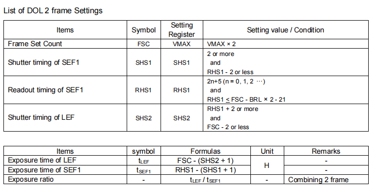
DOL two-frame settings and exposure formulas — original English figure, PDF page 222
| Item | Symbol | Setting register | Setting value / condition |
|---|---|---|---|
| Frame Set Count | FSC | VMAX | VMAX × 2 |
| Shutter timing of SEF1 | SHS1 | SHS1 | 2 or more and RHS1 - 2 or less |
| Readout timing of SEF1 | RHS1 | RHS1 | 2n+5 (n = 0, 1, 2 …) and RHS1 ≤ FSC - BRL × 2 - 21 |
| Shutter timing of LEF | SHS2 | SHS2 | RHS1 + 2 or more and FSC - 2 or less |
| Item | Symbol | Formula | Unit | Remarks |
|---|---|---|---|---|
| LEF exposure time | t_LEF | FSC - (SHS2 + 1) | H | - |
| SEF1 exposure time | t_SEF1 | RHS1 - (SHS1 + 1) | H | - |
| Exposure ratio | - | t_LEF / t_SEF1 | - | Combining 2 frames |
CISHdrTimeRegMin:
The minimum exposure value of long frames can be calculated through the table:
exposure of long frame = FSC-SHS2-1=FSC-(FSC-2)-1=1
exposure of short frame = RHS1-SHS1-1=RHS1-(SHS1-2)-1=1
So the minimum exposure behavior under HDR is 1
CISHdrTimeRegOdevity: From the table, shs1 and shs2 have no restrictions like 2n or 2n+1, so the corresponding exposure line can be incremented by 1
CISHdrTimeRegSumFac:
The sum of long and short frame exposures =(FSC-SHS2-1)+ (RHS1-SHS1-1)
SHS2 and SHS1 take the minimum value at the same time to maximize the exposure of both the long and short frames
The sum of long and short frame exposures =(FSC-(RHS1+2)-1)+ (RHS1-2-1)=FSC-6
For 2 frames of DOL hdr, FSC=2vts, so the maximum exposure sum of long and short frames is =2vts-6
That is, CISHdrTimeRegSumFac=[2 6], but for the convenience of calculation, Sony’s DOL hdr driver will use FSC as the aec uploaded by vts, that is, the uploaded vts has actually been doubled, so CISHdrTimeRegSumFac= [1 6]
CISTimeRegUnEqualEn=1
Whether the time of the long and short frames can be equal, due to the imx290 short frame limitation, it cannot be equal under any circumstances
CISHdrGainIndSetEn=1
Whether the gain of the long and short frames needs to be set to the same, 1 means it can be set to different values, 0 means the gain of the long and short frames must be the same, see the sensor description for details, some sensors share a set of registers for the long and short frames, and some sensors have different gains in the long and short frames. However, for design reasons, the two sets of registers need to be set to the same value. In order to expose the correctness of the decomposition, this parameter needs to be filled in accurately.
Note:
imx290 needs to pay attention to the setting of FPGC PFGC_1 value, the DOL document has specific description.
FullResolution=1920x1080
GainRange=1 2 20 20 1 0 20 2 4 10 0 1 20 40 4 8 5 -20 1 40 60 8 16 2.5 -40 1 60 80 16 32 1.25 -60 1 80 100 32 64 0.625 -80 1 100 120 64 128 0.3125 -100 1 120 140 128 256 0.15625 -120 1 140 160 256 512 0.078125 -140 1 160 180 512 1024 0.0390625 -160 1 180 200
IsLinear=0
The Rk platform supports the gain value setting in multiples and the gain value setting in the sony db mode. 0 means db is used. The db method can be used directly for imx290, or the above GainRange decomposition formula can be used. The GainRange decomposition formula will have a slight error, after all The non-linear curve is broken down into multiple linear curves.
NonLinear=DB_MODE
PatternMode=RGGB
TimeFactor=0 0 1 0.5
Time decomposition formula, it is recommended to keep this formula, if the calculation does not meet the formula, the sensor driver will do the conversion.
hdr_dcg_ratio=2
normal_dcg_ratio=2
Dcg ratio has been described above
SensorFlip=0
The default mirror flip state, bit0 mirror, bit1 flip
20. Appendix A CIS driver V4L2-controls list
| CID | description |
|---|---|
| V4L2_CID_VBLANK | Vertical blanking. The idle period after every frame during which no image data is produced. The unit of vertical blanking is a line. Every line has length of the image width plus horizontal blanking at the pixel rate defined by V4L2_CID_PIXEL_RATE control in the same sub-device. |
| V4L2_CID_HBLANK | Horizontal blanking. The idle period after every line of image data during which no image data is produced. The unit of horizontal blanking is pixels. |
| V4L2_CID_EXPOSURE | Determines the exposure time of the camera sensor. The exposure time is limited by the frame interval. |
| V4L2_CID_ANALOGUE_GAIN | Analogue gain is gain affecting all colour components in the pixel matrix. The gain operation is performed in the analogue domain before A/D conversion. |
| V4L2_CID_PIXEL_RATE | Pixel rate in the source pads of the subdev. This control is read-only and its unit is pixels / second. Ex mipi bus:pixel_rate = link_freq * 2 * nr_of_lanes / bits_per_sample |
| V4L2_CID_LINK_FREQ | Data bus frequency. Together with the media bus pixel code, bus type (clock cycles per sample), the data bus frequency defines the pixel rate (V4L2_CID_PIXEL_RATE) in the pixel array (or possibly elsewhere, if the device is not an image sensor). The frame rate can be calculated from the pixel clock, image width and height and horizontal and vertical blanking. While the pixel rate control may be defined elsewhere than in the subdev containing the pixel array, the frame rate cannot be obtained from that information. This is because only on the pixel array it can be assumed that the vertical and horizontal blanking information is exact: no other blanking is allowed in the pixel array. The selection of frame rate is performed by selecting the desired horizontal and vertical blanking. The unit of this control is Hz. |
21. Appendix B MEDIA_BUS_FMT table
| CIS sensor type | Sensor output format |
|---|---|
| Bayer RAW | MEDIA_BUS_FMT_SBGGR10_1X10 MEDIA_BUS_FMT_SRGGB10_1X10 MEDIA_BUS_FMT_SGBRG10_1X10 MEDIA_BUS_FMT_SGRBG10_1X10 MEDIA_BUS_FMT_SRGGB12_1X12 MEDIA_BUS_FMT_SBGGR12_1X12 MEDIA_BUS_FMT_SGBRG12_1X12 MEDIA_BUS_FMT_SGRBG12_1X12 MEDIA_BUS_FMT_SRGGB8_1X8 MEDIA_BUS_FMT_SBGGR8_1X8 MEDIA_BUS_FMT_SGBRG8_1X8 MEDIA_BUS_FMT_SGRBG8_1X8 |
| YUV | MEDIA_BUS_FMT_YUYV8_2X8 MEDIA_BUS_FMT_YVYU8_2X8 MEDIA_BUS_FMT_UYVY8_2X8 MEDIA_BUS_FMT_VYUY8_2X8 MEDIA_BUS_FMT_YUYV10_2X10 MEDIA_BUS_FMT_YVYU10_2X10 MEDIA_BUS_FMT_UYVY10_2X10 MEDIA_BUS_FMT_VYUY10_2X10 MEDIA_BUS_FMT_YUYV12_2X12 MEDIA_BUS_FMT_YVYU12_2X12 MEDIA_BUS_FMT_UYVY12_2X12 MEDIA_BUS_FMT_VYUY12_2X12 |
| Only Y (black and white) is raw bw sensor | MEDIA_BUS_FMT_Y8_1X8 MEDIA_BUS_FMT_Y10_1X10 MEDIA_BUS_FMT_Y12_1X12 |
22. Appendix C CIS Reference Driver List
| CIS interface | Output type | Frame / field | Reference driver |
|---|---|---|---|
| MIPI | Bayer RAW | frame | 0.3M: ov7750.c, gc0403.c 0.9M jx_h62.c 1.2M ov9750.c jx-h65.c 2M ov2685.c ov2680.c ov2735.c ov02g10.c ov02b10.c gc2385.c gc2355.c gc2053.c sc2232.c sc2239.c sc223a sc210iot.c sp250a.c 4M gc4c33.c jx_k04.c os04c10.c sc401ai.c 5M ov5695.c ov5648.c ov5670.c gc5024.c gc5025.c gc5035.c hm5040.c sc5239.c hynix_hi556.c 8M ov8858.c |
| CIS Data interface | CIS Output data type | Frame/Field | Reference drive |
|---|---|---|---|
| os08a10.c os08a20.c sc8220 imx378.c imx317.c imx219.c gc8034.c hynix_hi846.c s5kgm1sp.c s5k4h7yx.c 13M ov13850.c ov13b10.c imx258.c ov12d2q.c | |||
| MIPI | Bayer raw hdr | frame | 2M imx307.c imx327.c imx462.c gc2093.c ov02k10 ov2718.c sc200ai.c sc2310.c jx-f37.c 4M ov4689.c os04a10.c imx347.c imx464.c sc4238.c 5M imx335.c os05a20.c sc500ai.c 8M imx334.c imx415.c |
| MIPI | YUV | frame | 2M gc2145.c |
| CIS Data interface | CIS Output data type | Frame/Field | Reference drive |
|---|---|---|---|
| MIPI | RAW BW | frame | 0.3M ov7251.c 1M ov9281.c 1.3M sc132gs.c |
| MIPI | YUV | field | tc35874x.c |
| ITU.BT601 | Bayer RAW | 2M imx323.c ar0230.c | |
| ITU.BT601 | YUV | 0.3M gc0329.c gc0312.c gc032a.c 2M gc2145.c gc2155.c gc2035.c bf3925.c | |
| ITU.BT601 | RAW BW | 0.3M sc031gs.c 1.3M sc032gs.c | |
| ITU.BT656 | Bayer RAW | 2M imx323(Can support) |
23. Appendix D VCM driver ic reference driver list
| Reference driver |
|---|
| vm149c.c |
| dw9714.c |
| dw9718.c |
| fp5510.c |
| gt9760s.c |
| fp5501.c (step motor) |
| mp6507.c (step motor) |
| ms41908.c (step motor) |
24. Appendix E Flash light driver ic reference driver list
| Reference driver |
|---|
| sgm3784.c |
| leds-rgb13h.c (GPIO control) |