
This article uses the specified datasheet revision. Values are vendor specifications, not ArmSoM measurements; no new hardware validation was performed. Check the actual silicon revision, board schematic, SDK/BSP, kernel and drivers. The explanations and editable tables assist reading; consult the original PDF for the complete specification and bit definitions not expanded here.
RK730 · Rockchip RK730 Datasheet V1.0-20241118.pdf · PDF 44–46.
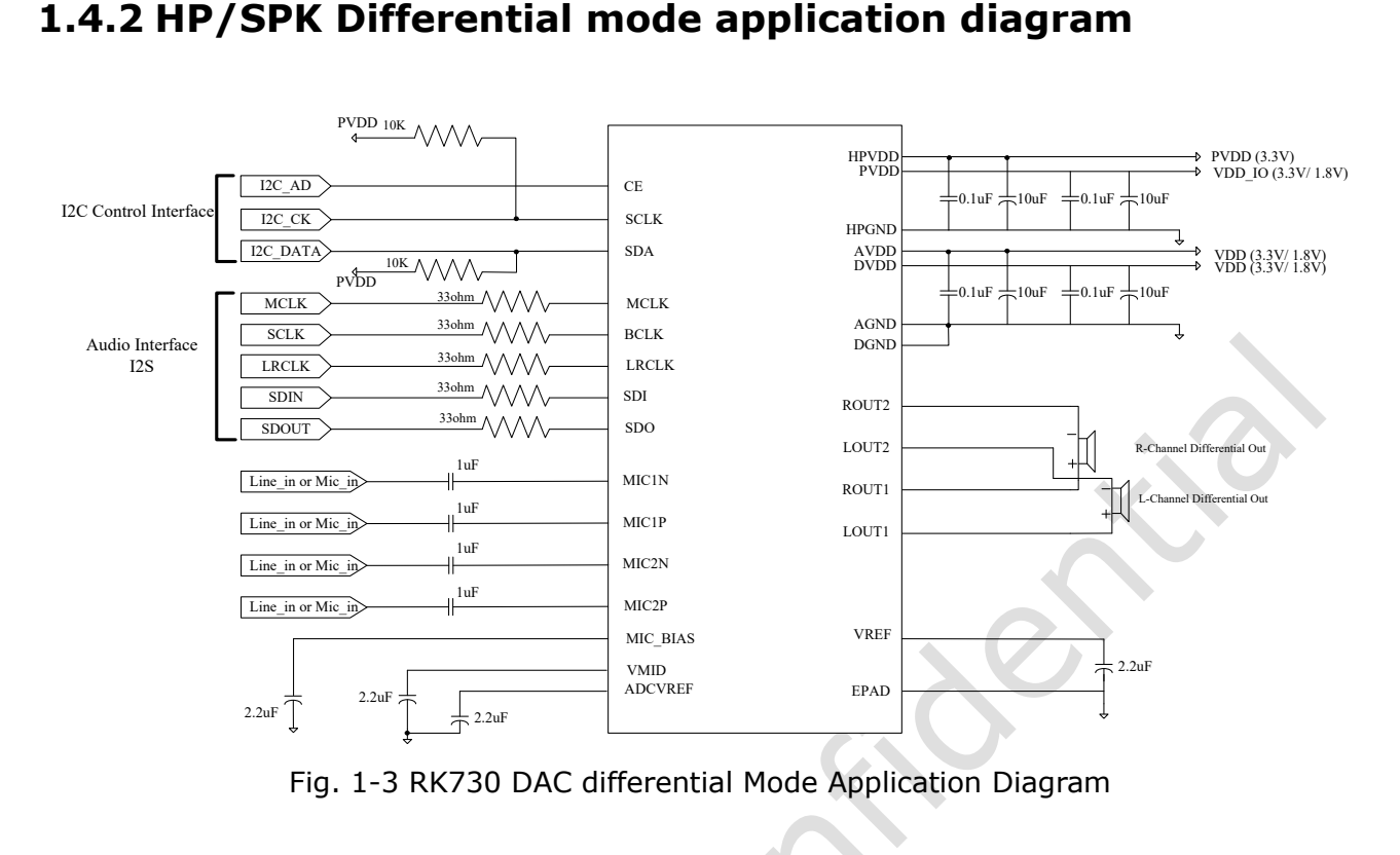
Original English figure, source PDF p. 10.
These are reference sequences, not an executable script
Tables follow pages 44–46 from top to bottom. A field assignment changes the named bits, not the entire register; preserve other bits and respect driver locking and power management. Delays not specified by the source are not invented. Check the current driver, clocks, channel mapping and analog circuit before use.
Six complete sequences
System power-up
| Reading order | Source label | Field assignment | Action / group |
|---|---|---|---|
| 1 | 0 | — | Apply analog and digital supplies |
| 2 | 1 | 0x1F[7]=1'b1 |
Enable LDO VMID |
| 3 | 2 | 0x10[7:0]=8'b00000000 |
System PLL control |
System power-down
| Reading order | Source label | Field assignment | Action / group |
|---|---|---|---|
| 1 | 0 | — | Keep supplies on; disable DAC and ADC first |
| 2 | 1 | 0x10[7:0]=8'b11111111 |
Power down system PLL |
| 3 | 2 | 0x1F[7]=1'b0 |
Disable LDO VMID |
| 4 | 3 | — | Remove analog and digital supplies |
Enable ADC
| Reading order | Source label | Field assignment | Action / group |
|---|---|---|---|
| 1 | 0 | — | Complete system power-up |
| 2 | 1 | 0x01[7]=1'b0 |
HK_TOP_1 |
| 3 | 2 | 0x0A[0]=1'b0 |
MIC_BOOST_0 |
| 4 | 3 | 0x0B[0]=1'b0 |
MIC_BOOST_1 |
| 5 | 4 | 0x0C[0]=1'b0 |
MIC_BOOST_2 |
| 6 | 5 | 0x0D[0]=1'b0; 0x0D[7:6]=2'b01 |
MIC_BOOST_3 |
| 7 | 6 | 0x0E[0]=1'b0 |
ADC_PGA_BLOCK_0 |
| 8 | 7 | 0x0F[0]=1'b0; 0x0F[7:6]=2'b01 |
ADC_PGA_BLOCK_1 |
| 9 | 8 | 0x04[1:0]=2'b00 |
ADC_0 |
| 10 | 9 | 0x06[4]=1'b1; 0x06[3]=1'b1 |
ADC_2 |
| 11 | 10 | 0x07[5:4]=2'b01 |
ADC_3 |
| 12 | 11 | 0x41[2:0]=3'b010 |
SRT |
| 13 | 12 | 0x44[7]=1'b1 |
VUCTL |
| 14 | 13 | 0x69[0]=1'b0 |
I2S_CKM |
| 15 | 14 | 0x6F[6]=1'b0 |
I2S_TXCR1 |
| 16 | 15 | 0x71[7:0]=8'b10001000 |
I2S_TXCMD |
| 17 | 16 | 0x40[7:6]=2'b11 |
DIGEN |
| 18 | 17 | 0x40[5:4]=2'b11 |
DIGEN |
| 19 | 18 | — | Start recording |
Disable ADC (original step labels preserved)
| Reading order | Source label | Field assignment | Action / group |
|---|---|---|---|
| 1 | 0 | — | Stop recording; keep channels temporarily |
| 2 | 1 | 0x40[5:4]=2'b00 |
DIGEN |
| 3 | 2 | 0x40[7:6]=2'b00 |
DIGEN |
| 4 | 3 | 0x71[7:0]=8'b00000000 |
I2S_TXCMD |
| 5 | 8 | 0x04[1:0]=2'b11 |
ADC_0 |
| 6 | 7 | 0x0F[0]=1'b1; 0x0E[0]=1'b1 |
ADC_PGA_BLOCK_1 / ADC_PGA_BLOCK_0 |
| 7 | 6 | 0x0D[0]=1'b1 |
MIC_BOOST_3 |
| 8 | 4 | 0x0C[0]=1'b1 |
MIC_BOOST_2 |
| 9 | 3 | 0x0B[0]=1'b1 |
MIC_BOOST_1 |
| 10 | 2 | 0x0A[0]=1'b1 |
MIC_BOOST_0 |
| 11 | 1 | 0x01[7]=1'b1 |
HK_TOP_1 |
Enable DAC
| Reading order | Source label | Field assignment | Action / group |
|---|---|---|---|
| 1 | 0 | — | Complete system power-up |
| 2 | 1 | 0x01[7:6]=2'b00 |
HK_TOP_1 |
| 3 | 2 | 0x41[6:4]=3'b010 |
SRT |
| 4 | 3 | 0x44[6]=1'b1 |
VUCTL |
| 5 | 4 | 0x69[7:0]=8'b00111010 |
I2S_CKM |
| 6 | 5 | 0x40[7:4]=4'b0101 |
DIGEN |
| 7 | 6 | 0x40[7:4]=4'b0000 |
DIGEN |
| 8 | 7 | 0x69[7:0]=8'b00000000 |
I2S_CKM |
| 9 | 8 | 0x6E[7]=1'b1 |
I2S_RXCMD |
| 10 | 9 | 0x40[3:0]=4'b0101 |
DIGEN |
| 11 | 10 | 0x40[3:0]=4'b1111 |
DIGEN |
| 12 | 11 | 0x4F[7:4]=4'b0000 |
DDAC_FILTER |
| 13 | 12 | 0x08[2:0]=3'b000 |
DAC_0 |
| 14 | 13 | 0x09[6:4]=3'b000 |
DAC_1 |
| 15 | 14 | 0x21[7:0]=8'b10000000 |
HP_0 |
| 16 | 15 | 0x24[7:0]=8'b10000000 |
SPK_0 |
| 17 | 16 | — | Start playback |
Disable DAC
| Reading order | Source label | Field assignment | Action / group |
|---|---|---|---|
| 1 | 0 | — | Mute first |
| 2 | 1 | 0x24[3:2]=2'b11 |
SPK_0 |
| 3 | 2 | 0x21[3:2]=2'b11 |
HP_0 |
| 4 | 3 | 0x09[6:4]=3'b111 |
DAC_1 |
| 5 | 4 | 0x08[2:0]=3'b111 |
DAC_0 |
| 6 | 5 | 0x40[3:0]=4'b0101 |
DIGEN |
| 7 | 6 | 0x40[3:0]=4'b0000 |
DIGEN |
| 8 | 7 | 0x6E[7]=1'b0 |
I2S_RXCMD |
| 9 | 8 | 0x01[7:6]=2'b11 |
HK_TOP_1 |
Numbering conflicts and page continuations
ADC shutdown labels are 0,1,2,3,8,7,6,4,3,2,1, with repeats and reversal. Original labels are preserved alongside reading order; they are not numerically sorted. ADC enable step 9 crosses a page, and both 0x06[4] and 0x06[3] are retained. DAC enable’s DIGEN transition from 0101 to 0000 is also preserved; do not collapse intermediate operations because final values repeat.
What board validation should record
Record supply rails, MCLK/BCLK/LRCLK waveforms, driver revision, sample settings and register differences around transitions. Check ADC with a known input amplitude, then DAC with a defined load; inspect mute, noise, pops and recovery. System shutdown disables audio paths before removing external supplies. These are validation recommendations, not a claim of completed ArmSoM testing.
ArmSoM products and application limits
CM1 and Forge1 are platform references for audio peripheral designs. This article does not claim an onboard RK730 or verified drop-in driver support. First check whether the required I2S, I2C, clocks and voltage levels are exposed.