
Based on the Chinese RK3588S Hardware Design Guide V1.2 (2023-12-14) for circuit and PCB review. CM7S carriers must follow module interface definitions; Sige7S supports software and peripheral evaluation. SoC capabilities are not a board connector list. Verify SDK/BSP, kernel, board revision, firmware and multiplexing. Values are source references, not ArmSoM hardware measurements.
RK3588S Hardware Design Guide V1.2 (2023-12-14), CN · §2.3.5; §3.4.7
Draw the mux matrix first
The two RK3588S SATA controllers use PIPE_PHY0 and PIPE_PHY2, shared with PCIe2.0; PHY2 also serves USB3 HOST2. The guide lists 1.5/3/6Gbps and Port Multiplier, not a guarantee that CM7S or Sige7S exposes both ports. Determine available channels from product documentation before choosing connectors and BSP settings.
Validate signals and drive power separately
The reference uses 10nF in both TX and RX, preferably 0201; do not copy PCIe capacitors. SATA_CP_DET, MP_SWITCH and CP_POD are shared control resources, so hot-plug requires deliberate design. Supply and test drive spin-up current externally; check sustained writes, errors, hot-plug and power-loss recovery.
Design parameters and review table
| Item | Source reference |
|---|---|
| SATA coupling | 10nF ±20%; TX and RX |
| Differential target | 100Ω ±10%; source fallback 90Ω ±10% |
| Length / intra-pair | <6in / <6mil |
| Recommended via count | Recommended ≤2 |
Source figures
No corresponding English design guide was found for this batch. All four editions use Chinese source screenshots with localized captions. Open an image for full resolution; the article text and parameter tables remain copyable. Page references are physical PDF pages.
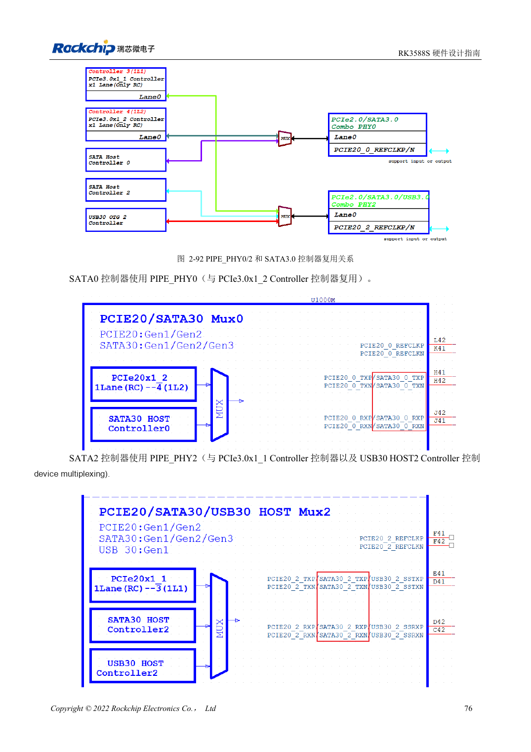
Chinese original · PDF 91 · 2-92
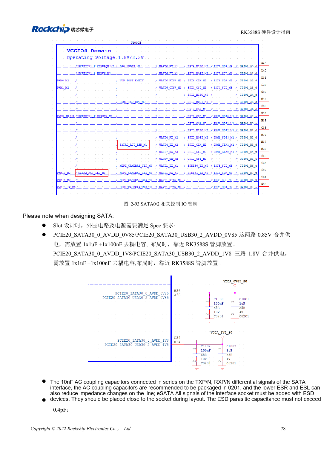
Chinese original · PDF 93 · 2-93
ArmSoM development path
CM7S supports custom carriers: first identify supplies, DDR and boot circuits already integrated in the module, then design outside its connectors. Sige7S provides a starting point for software and peripheral evaluation. For both products, verify exposed interfaces, pin assignments, levels, system images and cooling against the relevant revision. A chip reference schematic is not a product wiring diagram.