
Based on RK3506 Hardware Design Guide V1.0 (2024-09), covering G2 and B/J. Verify package, memory, rails and pins by variant and CM1/Forge1 interfaces against board documentation. This is an engineering topic article, not a complete page-by-page translation. Values are source references, not ArmSoM hardware measurements. Validate the actual SDK/BSP, kernel and firmware.
RK3506 Hardware Design Guide_V1.0_20240904_CN.pdf · §2.3.4–2.3.6; §3.3.3–3.3.4; §3.3.11
Select one display path first
The VOP has one port, supporting RGB/BT1120/BT656/MCU or MIPI, with a documented maximum of 1280×1280@60Hz. Interface names cannot be added together to promise simultaneous displays. LCDC belongs to VCCIO1 and must match the panel voltage; source-side 33Ω on HSYNC/VSYNC and 22Ω on CLK are recommended. MIPI DSI TX has two data lanes at 1.5Gbps/Lane. Reusing MIPI pins as GPO provides 1.8V outputs only, not general bidirectional GPIO.
USB ports and protection
Of the two USB2.0 OTG ports, preserve OTG0 for flashing. G2 does not expose OTG0 ID/VBUSDET, while B/J does; GPIO-based detection must avoid back-powering when the PC is connected but the board is off. Retain 2.2Ω in DP/DM and 100Ω in ID; use a current-limited switch for host 5V. The circuit chapter allows ESD capacitance up to 3pF, whereas the PCB chapter recommends ≤0.4pF. Keep both references visible and use the stricter budget with eye-diagram verification. USB routing: 90Ω±10%, intra-pair mismatch <20mil, length <6in, preferably at most four vias and never more than six.
RM_IO flexibility still has limits
RM_IO0–31 can select function ID0–98, but a given function maps to only one RM_IO pin. The matrix spans PMUIO and VCCIO1; avoid splitting timing-sensitive SAI/PDM/SPI across domains. An I2C split requires equal voltages, and PMUIO is fixed at 3.3V. MIPI PCB references are 100Ω±10% differential, intra-pair mismatch <6mil, data-pair to clock-pair mismatch <18mil, length <6in and preferably ≤4 vias. Build a signal/function/power-domain matrix before assigning the connector, then verify the complete channel rather than only bare-board length.
Source figures and review pages
Only Chinese originals are available in this batch. All four languages use the same source images, retaining figure context; image labels are not translated. Prose is editable. Page numbers are physical PDF pages.
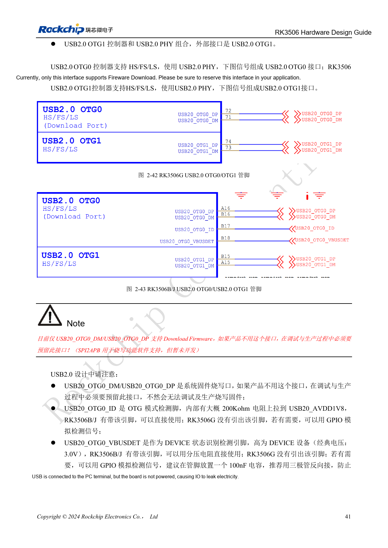
PDF 56
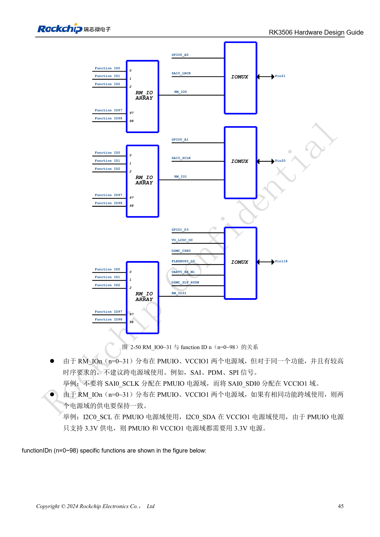
PDF 60
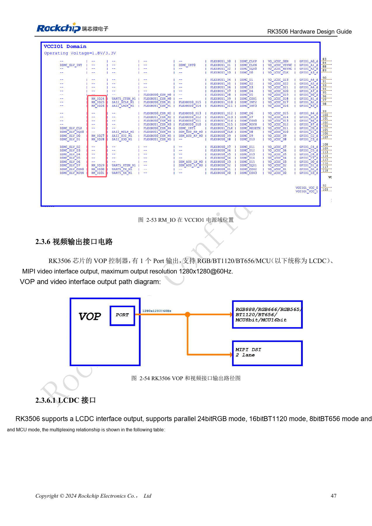
PDF 62
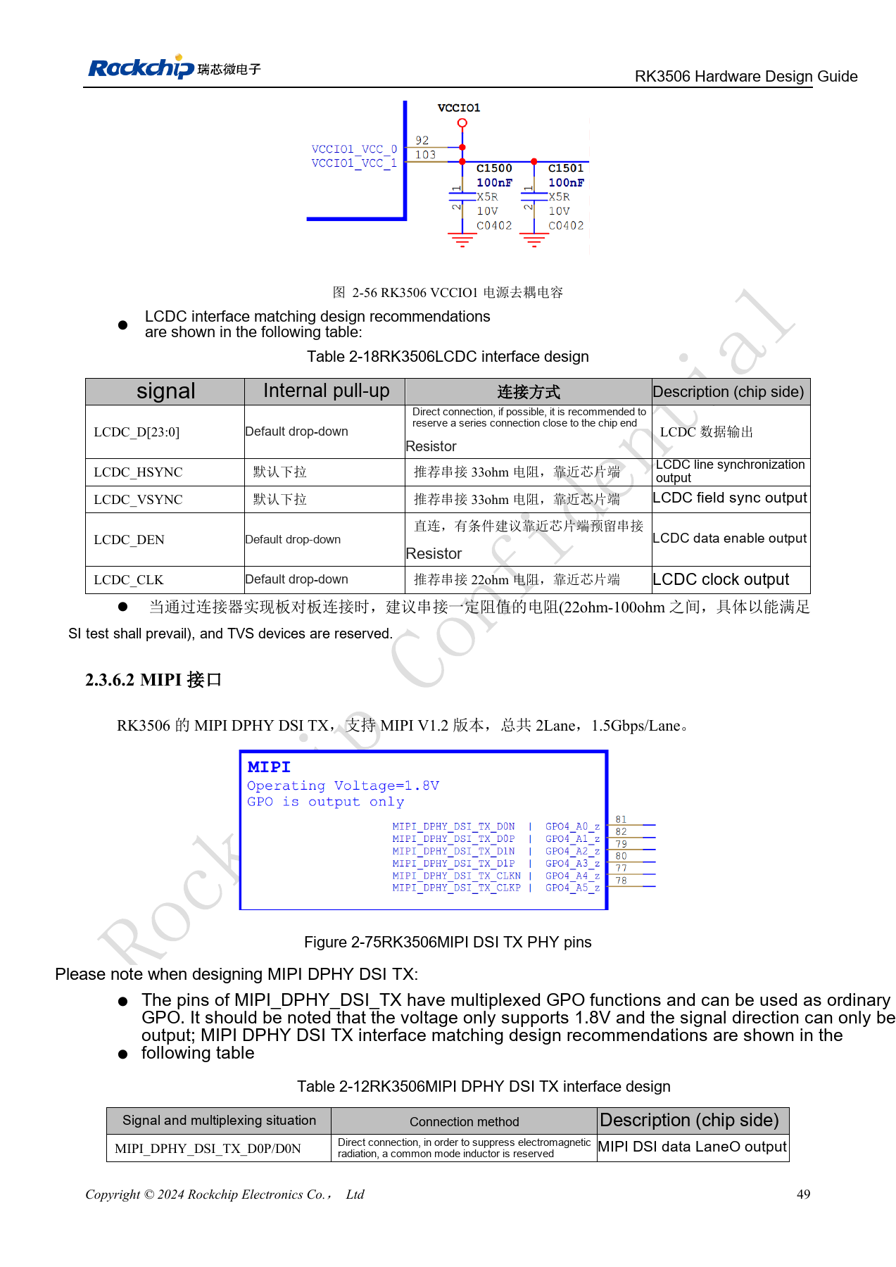
PDF 64
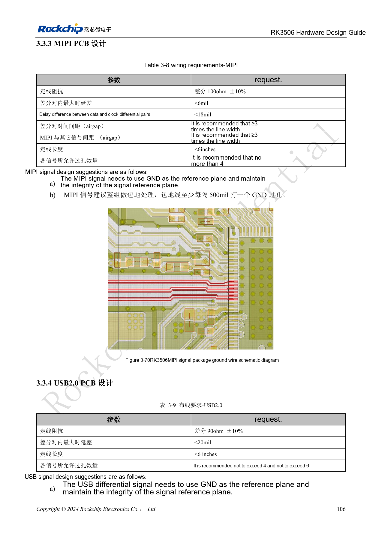
PDF 121
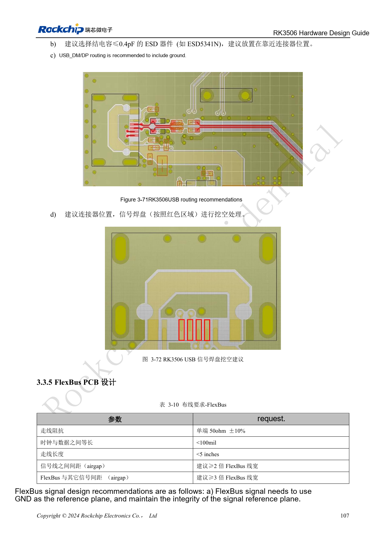
PDF 122
ArmSoM products and documentation
Continue reading
- Series contents
- RK3506 minimum system: clocks, reset and recovery
- RK3506 power domains: G2, B/J and carrier boundaries
- RK3506 DDR, eMMC and FSPI: circuits and routing
- RK3506 audio design: SAI, PDM, ASRC and DSM
- RK3506 industrial interfaces: RMII, FlexBus, DSMC and controls
- RK3506 thermal, ESD and production review