
The common baseline is the complete technical body of RK-SM-YF-017 Chinese V2.2.0, checked chapter by chapter against the English source with English-only material added. The English cover states V2.5.0, but its revision table stops at V2.2.0; the cover does not establish that all technical content is newer. Chinese uses Chinese original figures; English, Russian and German use English original figures. English-only supplementary figures are explicitly attributed in all languages. The source lists “all products” without a kernel version; this does not establish support for every ArmSoM board. This is a platform reference: verify the actual SoC, storage controller and device, SDK/BSP, BOOTROM, Loader, U-Boot, kernel and partition scheme. No ArmSoM hardware validation was performed. Vendor test descriptions and prices are source information and historical examples, not ArmSoM measurements, current quotations or supply commitments.
Safety: erasing, programming, efuse/OTP, repartitioning and Vendor ID writes may cause data loss or irreversible changes. The example writes ID 1 (SN); do not run it on production devices. Back up device identity and firmware first. This page executes no commands.
ArmSoM Docs · Rockchip Linux kernel · EDITORIAL-NOTES
Additional source references (partitions, U-Boot, Vendor Storage, production programming, open-source flash and dual storage, respectively):
Rockchip_Introduction_PartitionRockchip-Developer-Guide-UBoot-nextdev-CNRK Vendor Storage Application NoteRockchip量产烧录指南_v1.2Rockchip_Developer_Guide_Linux_Flash_Open_Source_Solution_CNRockchip_Developer_Guide_Dual_Storage_CN
Source differences and treatment
The tables below consistently follow the approved Chinese V2.2.0 baseline. Conflicting values are not silently replaced with English ones:
- §2.3: Chinese lists SPI NOR packages as
5x4 SOP8/8x6 WSON; English page 9 lists only5x4 SOP8. The fuller Chinese entry is retained. - §2.8: English page 17 specifies SLC NAND / Nand V6 ECC as
16 bits per 1KB; the Chinese table says16bits ECC, while its §3.1 prose separately says16bits/1KB. This English clarification is retained here without rewriting the source table. - §4.1: Chinese page 23 gives RK2108 SD Boot as
N, versusYon English page 25. Chinese gives RK3328 and RK3399 EMMC/NAND Boot asY/N, whereas English givesN/Yfor both. RK3399 SPI NAND isY*1in Chinese andYin English. The Chinese row namedRK3229corresponds toRK3228in English. These source conflicts require verification; neither table certifies board boot support. - §4.2: English page 26 additionally qualifies the RK3568/RK3566 USB1 cell as
3.0 OTG (RK3568 Only); Chinese page 25 says only3.0 OTG. Retain the English restriction for adaptation checks rather than infer general RK3566 capability. - §4.3: Both source boot-order tables contain
EMMC--; this is preserved pending clarification. Diagram breaks originate in PDF pagination; both parts are retained without redrawing or guessing connections. - §7.2: The table path
drivers/rkandconflicts with the later./drivers/rk_nand/. Both are preserved. API namesvendor_storage_readandrk_vendor_write, and code strings such as% sand% x, are also retained; examples are not certified directly compilable or safe to execute. - §6.1.4–6.1.5: Both sources compare the Linux tool with the “Android tool”; this has not been changed to Windows. The original “read-back call” wording for
RB_CHECK_OFFand its flag polarity are unclear; do not infer configuration values from its name.
1. Naming conventions
| Name | Description |
|---|---|
| SPI Nand | NAND over SPI, mostly SLC NAND |
| SPI Nor | NOR over SPI |
| PP Nand | Parallel peripherals NAND; parallel NAND, SLC\MLC\TLC NAND |
| Flash | Collective term for SPI NAND, SPI NOR and PP NAND |
| Nand | Collective term for NAND devices including SPI NAND and PP NAND |
| Octal SPI DTR Nor flash | Octal SPI NOR flash with double-data-rate sampling |
| OCTA flash | Octal SPI flash, including Octal SPI NOR and Octal SPI NAND |
2. Introduction to flash
2.1 Flash storage types
In the broad sense, flash includes all non-volatile storage based on NAND flash and NOR flash technology, such as EMMC and SPI flash commonly used in RK devices, as well as PCIe SSD, SATA SSD and UFS that have become more familiar in recent years. The following introduction explains their differences. A storage device mainly comprises two parts: the storage die and the interface controller, commonly called die and controller.
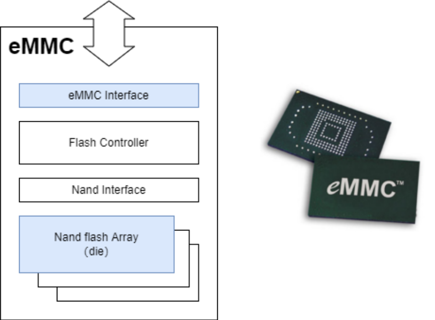
2.1 Flash storage types: original English source, page 7
The flash die ultimately stores user data, as illustrated by the NAND Flash Array in the figure. Manufacturers produce dies of different capacities and combine them with different controllers to form storage devices for different industries. For example, a NAND flash die with an EMMC interface becomes an EMMC device, and a NOR flash die with an SPI interface becomes an SPI flash device. Like the RK chip, these storage devices generally also run internal firmware. Some storage-device implementations are described below:
| Device | Device composition | Host controller | Special host-side software |
|---|---|---|---|
| SPI Nor | NOR + SPI interface | FSPI/SPI controller | Relatively simple: a filesystem with wear leveling and out-of-place updates is sufficient |
| PP Nand | NAND + parallel interface | NandC controller | FTL algorithm or filesystem with FTL |
| SPI Nand | NAND + SPI interface | FSPI/SPI controller | FTL algorithm or filesystem with FTL |
| eMMC | NAND + EMMC interface + FTL algorithm | SDMMC/SDHCI controller | MMC protocol framework |
| SD card | NAND + SDIO interface + FTL algorithm | SDMMC controller | MMC protocol framework |
| SATA SSD | NAND + SATA interface + FTL algorithm | Sata controller | SATA protocol framework |
| NVMe SSD |
NAND + PCIe interface + FTL algorithm | PCIe controller | NVMe protocol framework |
| UFS | NAND + UFS interface + FTL algorithm | UFS controller | UFS protocol framework |
| … |
Notes:
- Flash devices evolve toward faster interface controllers, greater internal parallelism and larger capacities.
- Besides the common storage types above, RK products have also supported SD NAND in surface-mount packages.
- All devices based on NAND flash require an FTL algorithm to manage NAND; the reasons are explained in “Basic Principles of NAND”.
- PP NAND and SPI NAND do not integrate their own FTL algorithm, so the host software must provide an FTL algorithm or a filesystem that includes one.
The following figure explains the relationship between die manufacturers, storage brands and RK controllers:
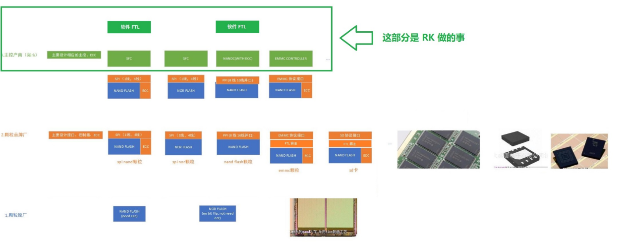
2.1 Flash storage types: original English source, page 9
English-source addition (page 9): dependence of MLC/TLC NAND on FTL, NandC SoC area cost and PP NAND pin count led RK to phase out the PP NAND interface; the source consequently describes its current flash products as mainly SPI flash. This is source-platform background, not a claim about every current ArmSoM product.
2.2 Selecting flash
SLC NAND, SPI NAND and SPI NOR: use the GigaDevice selection reference to understand the range of flash components. See the GD component selection reference link.
2.3 Brief comparison of flash types
A simple comparison of several RK primary storage types:
| Storage type | Stability | Unit price | Common dimensions and package | I/O rate | Common capacity |
|---|---|---|---|---|---|
| EMMC | Good | High | 13x11.5 153 FBGA | 200M DDR (HS400) |
>= 1GB |
| SLC Nand | Nornal | Nornal | 20x12 TSOP48 | 30M SDR | 128MB~512MB |
| SPI Nand | Nornal | Low | 8x6 WSON | 133M SDR 80M DDR |
64MB~512MB |
| SPI Nor | Good | Low | 5x4 SOP8/8x6 WSON | 166M SDR 104M DDR |
<= 128MB |
| Octal SPI Nand | Nornal | High | 8x6 24-BALL TFBGA | 120M DDR | 128MB~512MB |
| Octal SPI Nor | Good | High | 8x6 24-BALL TFBGA | 200M DDR | <= 128MB |
Notes:
- EMMC offers large capacity, relatively high stability and fast reads/writes, but costs more per device, uses a larger package and has greater initialization overhead, usually hundreds of milliseconds.
- SPI NAND offers a small package, low unit cost and greater capacity than NOR flash. However, ECC and storage-management algorithm requirements limit its read/write performance and stability to a generally average level.
- SPI NOR offers a small package, high stability, low unit cost and little software initialization overhead. Its loading speed is particularly good for small firmware, but continuous transfer is slower than EMMC, and device cost becomes higher at larger capacities.
- Because MLC/TLC PP NAND depends on FTL, the NandC controller occupies more chip area and needs many pins, RK has phased out PP NAND interfaces in recent years. Small-capacity storage therefore mainly means SPI flash, and MLC/TLC PP NAND is omitted from the table above.
- Prices are per device only; cost per MB decreases as capacity increases.
2.4 Common flash packages
Comparison of several packages:
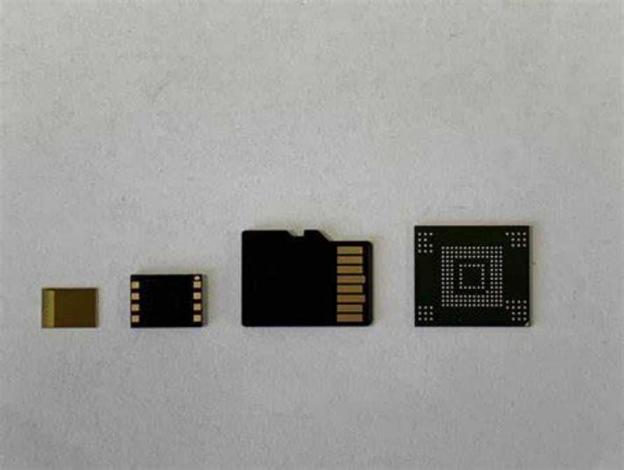
2.4 Common flash packages: original English source, page 10
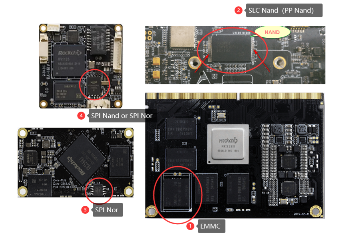
2.4 Common flash packages: original English source, page 11
Common SLC NAND / SPI flash packages:
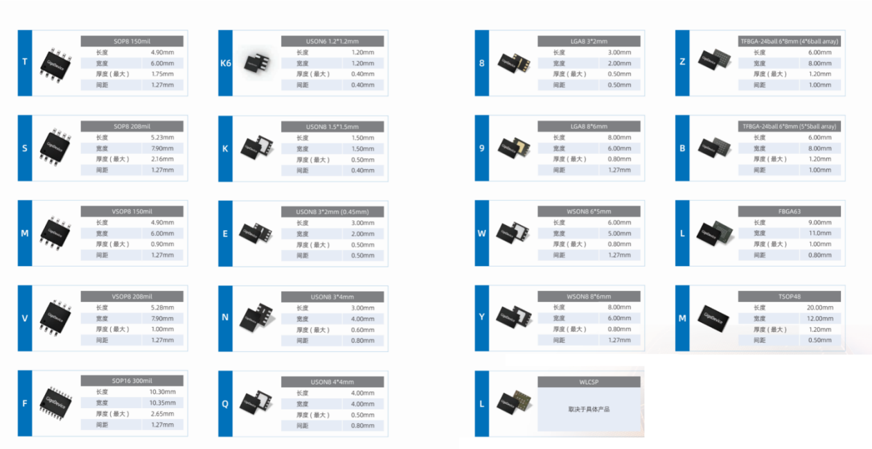
2.4 Common flash packages: original English source, page 11
Package introduction
2.5 Flash prices
| Storage type | Capacity | Price (USD) |
|---|---|---|
| SPINand | 1Gbits QPI Consumer | 0.53 |
| SPINand | 2Gbits QPI Consumer | 0.75 |
| SPINand | 4Gbits QPI Consumer | 1.7 |
| SPI NAND (limited component choice for Continuous read mode) | Compared with devices of the same capacity | Approximately +30% |
| PP | 1Gbits QPI Consumer | 0.6 |
| PP | 2Gbits QPI Consumer | 1.7 |
| PP | 4Gbits QPI Consumer | 3.8 |
| Nor | 32Mbits QPI Consumer | 0.15 |
| Nor | 64Mbits QPI Consumer | 0.19 |
| Nor | 128Mbits QPI Consumer | 0.35 |
| Nor | 256Mbits QPI Consumer | 1.0 |
| Nor | 512Mbits QPI Consumer | 2.5 |
| Nor | 1Gbits QPI Consumer | 5.5 |
| Nor | 2Gbits QPI Consumer | 11.5 |
| Nor | 256Mbits OPI Auto | 2.1 |
| Nor | 512Mbits OPI Auto | 3.6 |
Notes:
- The prices above are market quotations from specific manufacturers and exclude any markup for customer communication.
- They mainly illustrate price differences between storage types and the trend of increasing price with capacity within the same type.
2.6 Basic principles of NAND
Physical structure of a NAND flash array, using a common SLC NAND structure as the example:
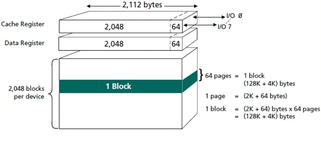
2.6 Basic principles of NAND: original English source, page 13
Notes:
- SLC NAND consists of multiple flash blocks, usually 1024, 2048 or 4096; the figure shows 2048 blocks.
- A block is the smallest erase unit. SLC NAND blocks are usually 128KB or 256KB; erasing changes logical 0 to 1.
- A block usually contains 64 pages; some devices have up to 128 pages.
- A page is the basic NAND programming/read unit. SLC NAND page size is usually 2KB or 4KB; programming changes logical 1 to 0.
- Logical 0 and 1 are physically voltage levels in each bit cell.
The following example uses SLC NAND implemented with a floating gate:
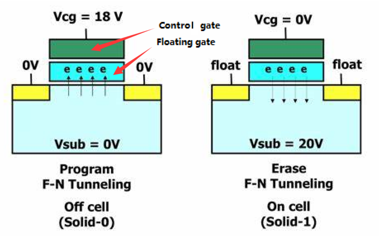
2.6 Basic principles of NAND: original English source, page 14
The internal floating gate is where flash actually stores data. Voltages applied to the control gate and substrate determine whether charge enters or leaves the floating gate. A logical 0 or 1 depends on whether the stored-charge voltage exceeds a particular threshold Vth:
- NAND programming charges the floating gate by applying a high voltage to the control gate. Above Vth, it represents 0.
- Data retention: charge enters the floating gate under high voltage and remains without erasure, but the electric field between gate and substrate causes gradual charge loss over time.
- P/E cycle: as Program/Erase cycles increase, the oxide between floating gate and substrate ages, affecting charge retention.
- NAND erasure discharges the floating gate by applying a high substrate voltage. Below Vth, it represents 1.
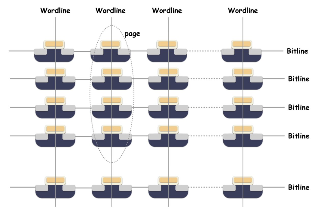
Wordline and Bitline design: to charge/discharge thousands of NAND cells efficiently, auxiliary Bitline/Wordline circuits are used. Cells connect in series to form NAND strings. A string terminates at the Bit Line and Source line; each cell control gate connects to a Wordline. Cells controlled by the same Wordline form a logical page. Together they form a block, whose cells share the substrate, so the smallest erase unit is a block.
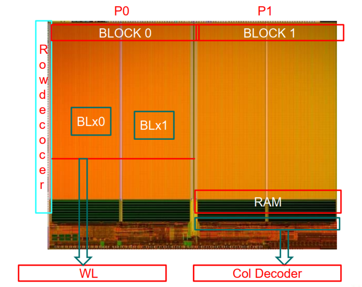
2.6 Basic principles of NAND: original English source, page 15
2.6 Basic principles of NAND: original English source, page 15
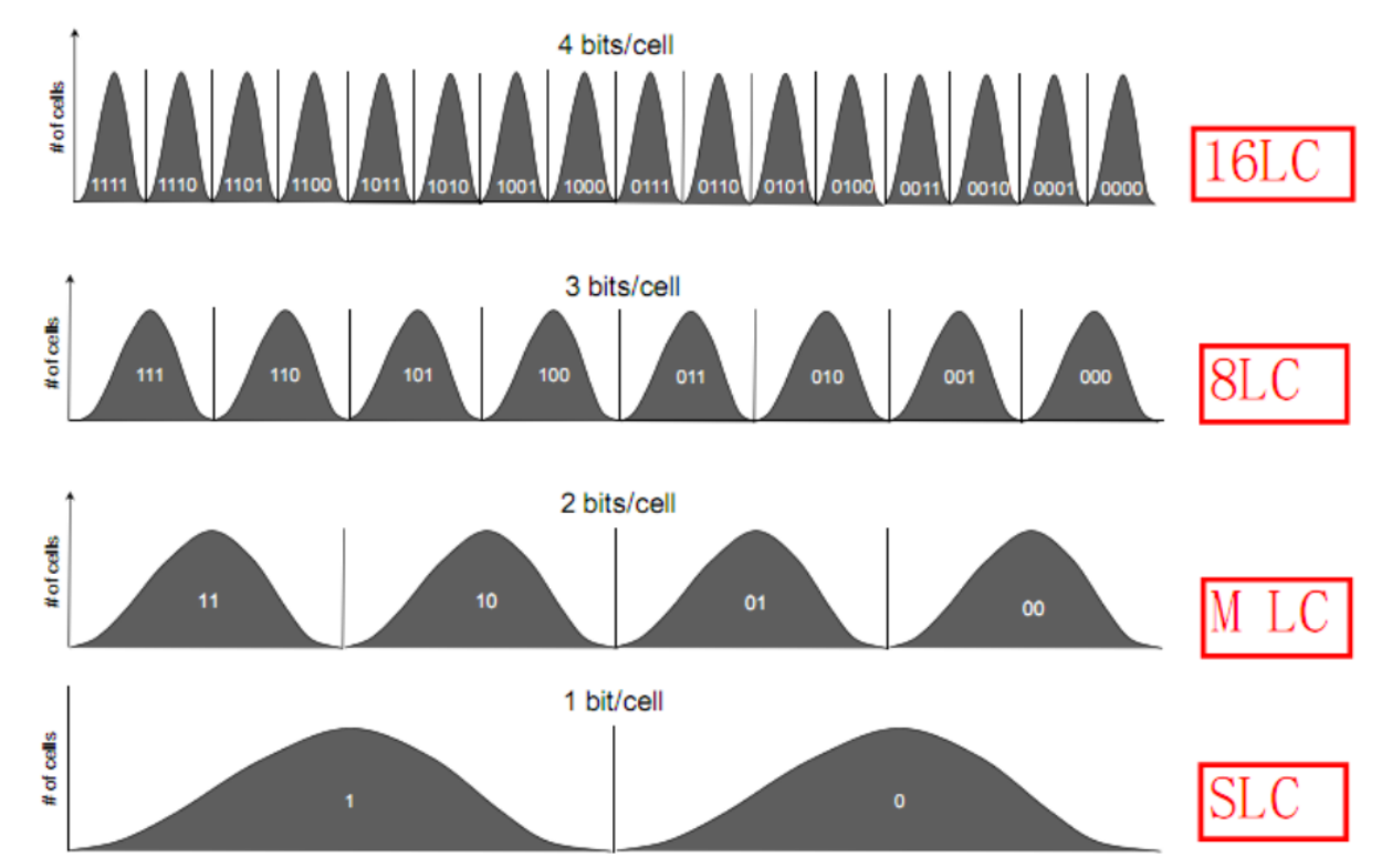
Bitline image source. Basic SLC/MLC/TLC/QLC principles: Bitline controls charging and discharging and thus the bit-cell level. Controlling charge quantity also allows one bit cell to represent different levels:
- SLC (Single Level Cell): 1 bit per cell, two logic levels 0/1.
- MLC: 2 bits, four levels 0–3.
- TLC: 3 bits, eight levels 0–7.
- QLC: 4 bits, sixteen levels 0–15.
2.6 Basic principles of NAND: original English source, page 16
Image sourced from the Internet.
Bit-cell charge-storage failure causes bit flips. The physical structure of NAND means unstable voltage during charging/discharging and physical aging from program/erase wear can impair charge retention. Logical levels can then change, producing bit flips. Users may see incorrect data, abnormal firmware behavior or filesystem corruption. NAND products therefore incorporate ECC algorithms of different strengths to extend device life and improve robustness.
NAND product characteristics follow from these physical principles:
- Out-of-place update: NAND programming changes a cell only from 1 to 0, so erasure is required before reprogramming. Programming operates on pages, whereas erasure operates on blocks containing multiple pages. Updating the same logical address at the same physical location would require erasing on every update. Because erasure takes time and wears flash, FTL generally maps updated data to a new location.
- Limited P/E endurance: each NAND block has a finite erase-cycle limit. After enough erasures the block becomes unstable, written data becomes error-prone, and erasure may fail. Older-process SLC NAND commonly reached 100K cycles, whereas newer processes introduced to reduce manufacturing costs may have lower endurance.
- Better performance: unlike a mechanical disk, flash has no mechanical mechanism or seek requirement, so address access overhead is similar everywhere. SSD random-read performance is therefore much better than that of a mechanical disk. Although this suggests equal random and sequential access speeds, flash supports cache operations: sequential reads can fetch the next page into internal registers in advance, responding faster. Sequential access is therefore faster than random access.
- Unequal read/write speeds: injecting electrons into the floating gate (writing) takes longer than detecting its electric-field state (reading). FTL therefore tries to minimize writes and erasures.
2.7 Basic principles of NOR
NOR follows principles similar to NAND, with these main differences:
- The bit-cell mechanism is similar, but both ends of each cell connect directly to Bit Line and Source line. This is more stable, so NOR generally does not need ECC to counter physical aging, although very rare bit flips remain possible. The surrounding circuitry is more complex, making the die more expensive at the same capacity.
- Block/page sizes differ from NAND.
- The usual erase units are Block and Sector, 64KB and 4KB respectively.
- The usual basic programming unit, page, is 256B.
2.8 NAND dependency on ECC
RK integration:
| Device type | Host controller | ECC provided by |
|---|---|---|
| EMMC | No host ECC required | EMMC device |
| SPI Nand | No ECC | SPI NAND device |
| SLC Nand | Nand V6 uses 16-bit ECC | NandC controller |
| MLC TLC Nand | Nand V9 uses 16-bit or stronger ECC | NandC controller |
Note: some SLC NAND devices include ECC. Other PP NAND devices do not integrate ECC and depend on the controller ECC.
2.9 Factory bad blocks in NAND
Because of NAND flash physical characteristics, manufacturing permits a proportion of factory bad blocks. Factory bad-block markers are written into a designated flash area, usually the first spare byte (also called the OOB area). These markers normally must not be destroyed. W25N01GV SPI NAND is an exception.
2.10 NAND endurance and ECC errors
NAND flash endurance is usually characterized by P/E (erase/write) cycles. Devices may fail after a certain count. In the source tests, some poor-quality devices showed abnormalities around 30K cycles. If this differs from the manufacturer specification, customers are advised to contact the manufacturer for diagnosis.
Near end of life, warnings typically include:
- Read-data bit flips reach the level requiring a refresh.
- Data remains valid and operation is normal.
At or beyond NAND lifetime, possible abnormalities include:
- Read-data bit flips require a refresh; data is still valid and operation normal.
- Read data reports ECC fail: data is invalid. Low-level retries may cause high thread CPU usage.
- Partial data loss leads to upper-layer faults.
- Erase/write failure: the block is marked bad without affecting use or losing data.
2.11 Key technologies in NAND FTL algorithms
- Address mapping: a flash device is a black box containing NAND flash and FTL. Applications use logical addresses, which FTL maps to physical addresses while tracking the latest data location for every logical address.
- Garbage collection: as data is written, some data in blocks becomes invalid. Valid data is moved away and the block is erased to receive new data.
- Wear leveling and bad-block management: each block has limited P/E endurance. Some blocks might otherwise be repeatedly used and damaged, while rarely accessed blocks remain untouched. FTL therefore balances use through garbage collection and free-block-pool management; ideally all blocks reach their wear threshold together. Because flash contains factory bad blocks and additional blocks may degrade during use, FTL avoids unusable blocks and promptly copies data from unstable blocks to stable locations.
2.12 Evolution of NAND solutions (PP NAND and SPI NAND)
- Early RK products supported only the closed-source FTL solution rkflash, mainly RK3326, RK3308 and RV1108.
- Customer needs for UBIFS, MTD and programmer-based flashing required the MTD storage-driver framework.
- Starting with RK3308, the drivers, algorithms and filesystem in this approach are open source; it is therefore distinguished internally from the closed-source solution as the MTD open-source solution.
- RK3308 supplies the low-level driver; capable customers integrate the upper layers themselves.
- The RK3308 product team previously supplied SDK configuration for a PP SLC NAND MTD open-source solution.
- SDKs then moved fully to MTD open source with more detailed support and guidance:
RV1126, RK3568 and later chips.
2.13 Flash host controllers
2.13.1 SFC controller
The Serial Flash Controller (SFC) controls data transfer between the chip system and serial NOR/NAND flash devices. Features:
- SPI NOR and SPI NAND support.
- 1-, 2- and 4-wire SPI NOR transfers.
- DMA transfers.
2.13.2 FSPI controller
FSPI (Flexible Serial Peripheral Interface) is a flexible serial-transfer controller and a new SFC design. Its name was changed to reflect the changed range of supported devices. Main features:
- SPI NOR, SPI NAND, and SPI-protocol PSRAM and SRAM.
- 1-, 2- and 4-wire SPI NOR transfer; version 8 and later support 8-wire DDR transfer.
- XIP technology.
- DMA transfer.
2.13.3 NandC controller
NandC transfers data between NAND flash and the main chip, supporting direct transfers as an AHB-bus master. RK mainly has two versions for different applications: the richly integrated NandC V9 and the simplified, smaller-area NandC V6. A chip generally selects its NandC version according to market positioning. NandC V6 supports only SLC NAND and is usually used for small-capacity storage products, generally SLC NAND below 512MB. NandC V9 supports MLC and TLC and can serve larger-capacity storage products.
2.13.4 General-purpose SPI interface
FSPI is a dedicated SPI flash interface. RK SoCs generally also have several general-purpose SPI interfaces that can connect external SPI flash, but devices on those interfaces normally cannot serve as bootdev.
2.14 SPI flash output-delay statistics
Summary:
| 1.8 V | 3.3 V | 1.65-3.6 | |
|---|---|---|---|
| FORESEE | < 8 ns | ||
| BIWIN | < 9 ns | ||
| Dosilicon | <10 ns | <8 ns | |
| ESMT | <8 ns | ||
| Toshiba | <6 ns | ||
| WINBONG | <7 ns | ||
| MXIC | <8 ns | ||
| MXIC (SPI NOR) | <12 ns(30 pf)<10 ns(15 pf) |
Note: consult the actual device datasheet; this table is for reference only.
3. Storage-device validation
3.1 Overview of SLC NAND/SPI NAND/SPI NOR validation
Verification explanation: small-capacity devices are relatively stable and generally have good compatibility with the main controller. Most therefore receive functional verification only; their reliability and stability mainly depend on extensive manufacturer testing and reports.
1. Functional verification
2. Basic product-lifecycle reliability verification
3. Software compatibility and stability verification
| Storage type | Functional validation | Device reliability validation | Software compatibility and stability validation |
|---|---|---|---|
| SPI Nor | Y | N*1 | N |
| SPI Nand | Y | Y | TBD*2 |
| SLC Nand | Y | N*3 | TBD*2 |
Notes:
1. SPI NOR receives functional verification only because it is relatively stable and compatible, and boundary behavior requires a very large test volume. Reliability and stability are guaranteed by the component manufacturer.
2. TBD: corresponding tests are performed only for devices with major compatibility changes or substantially updated storage-driver versions. Usually these tests are not performed.
3. For SLC NAND, ECC is mainly provided by the RK NAND controller, with correction up to 16bits/1KB. This provides large redundancy and high stability, so no further device-reliability verification is performed; reliability and stability are guaranteed by the manufacturer.
Verification methods:
1. Functional verification: controller compatibility, successful system boot, normal basic functions and a passed flash stress test of 10 loops.
2. Device reliability verification. Retention test: after applying a certain proportion of P/E cycles to flash, perform a high-temperature burn-in test to simulate product life.
3. Unexpected-power-loss verification for software compatibility and stability; testing on the actual product is recommended.
Power-loss test:
- Cut power once per minute.
- Boot into Linux after power-on.
- During powered operation, continuously read/write with dd without comparison, mainly testing FTL data migration integrity.
Continue for 7 days, meeting the basic needs of most products: approximately 10K read/write operations and around 10,000 power cuts.
3.2 Overview of RK flash sample-submission requirements
3.2.1 Validation prerequisites
General information:
1. Small-capacity storage includes SLC PP NAND, SPI NAND and SPI flash.
2. Prioritize submission of mainstream devices currently on sale.
3. This channel verifies drivers; it does not currently provide business-related recommendations.
4. The small-capacity storage support list is usually updated every 1–2 months. Actual device-verification time varies, but verification is completed before the list update.
5. Submit at least 10 pcs together with the corresponding device datasheet.
6. Prioritize devices urgently needed by customers.
Special notes for SPI NAND:
1. The device must include its own ECC module; otherwise it is unsupported because the RK controller does not integrate an ECC module.
2. There must be no consecutive bad blocks at the flash tail, or the tail bad-block-table information will be damaged. If this cannot be resolved, the device cannot be supported.
3. An odd-plane block must be selectable without plane-select bits. Some devices use a two-plane structure and require plane-select bits in the transmitted address to select odd-plane data. Such devices have RK-platform compatibility issues requiring driver adaptation and are not recommended.
Special notes for SPI NOR:
1. SPI NOR requires tRST shorter than 200us.
3.2.2 Validation procedure
Internal functional and stress tests verify compatibility between device and controller. Device stability and stress-test performance remain subject to the manufacturer specification. Verification is performed only on representative platforms. RK small-capacity storage controllers use compatible IP, so RK3568 verification covers most SoCs with the corresponding controller. For example, SPI NAND verified on RK3568 is compatible with RV1126 and RK3308.
3.2.4 Customer patch delivery
New flash components, especially SPI flash, normally require a source-code patch after verification. Customers needing driver support should raise an issue on the RK Redmine feedback platform; a patch package will then be provided online.
4. Device boot flow
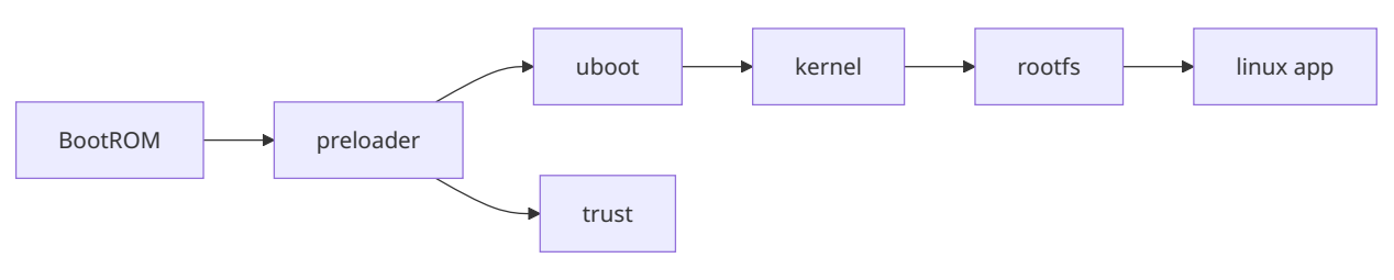
The boot process is the software sequence from system power-on to completed startup. The following figure shows Linux startup:
4. Device boot flow: original English source, page 24
4.1 RK SoC BOOTROM boot support
| Chip | Emmc Boot | Nand Boot | SPI NAND Boot | SD Boot | SPI NOR Boot |
|---|---|---|---|---|---|
| RV1108 | Y | Y | Y | Y | Y |
| RV1126/RV1109 | Y | Y | Y | Y | Y |
| RK2108 | Y | N | N | N | Y |
| RK2206 | Y | N | N | Y | Y |
| RK3036 | Y | Y | Y | Y | Y |
| RK3126C | Y | Y | Y*1 | Y | Y |
| RK3128 | Y | Y | Y | Y | Y |
| RK3229 | Y | Y | Y*1 | Y | Y |
| RK3288 | Y | Y | Y | Y | Y |
| RK3308 | Y | Y | Y | Y | Y |
| RK3326/PX30 | Y | Y | Y*1 | Y | Y |
| RK3328 | Y | N | Y*1 | Y | Y |
| RK3368/PX5 | Y | Y | Y*1 | Y | Y*1 |
| RK3399 | Y | N | Y*1 | Y | Y |
| RK3568/RK3566 | Y | Y | Y | Y | Y |
| RK3588 | Y | N | Y | Y | Y |
| RV1106/RV1103 | Y | N | Y | Y | Y |
| RK3528 | Y | N | Y | Y | Y |
| RK3562 | Y | N | Y | Y | Y |
*1: supported by chip hardware but not by the released SDK development package.
4.2 RK SoC storage-interface specifications
| AP | NANDC | SPI0 | SPI1 | SPI2 | SFC | SD | SDIO | EMMC | USB0 | USB1 |
|---|---|---|---|---|---|---|---|---|---|---|
| RK3188 | 60bits MLC SLC |
Boot | - | - | SD 3.0 |
SDIO 3.0 |
SD50 DDR50 |
2.0 Host | 2.0 OTG | |
| RK3128 | 60bits MLC SLC |
- | - | Boot | SD 3.0 |
SDIO 3.0 |
SD50 DDR50 |
2.0 Host | 2.0 OTG | |
| RK3126 | 60bits MLC SLC |
- | - | Boot | SD 3.0 |
SDIO 3.0 |
SD50 DDR50 |
2.0 Host | 2.0 OTG | |
| RK3036 | 60bits MLC SLC |
- | - | Boot | SD 3.0 |
SDIO 3.0 |
SD50 DDR50 |
2.0 Host | 2.0 OTG | |
| RK3288 | 60bits MLC SLC |
Boot | - | SD 3.0 |
SDIO 3.0 |
HS200 | 2.0 Host | 2.0 OTG | ||
| RK3399 | - | - | Boot | - | - | SD 3.0 |
SDIO 3.0 |
HS400 HS200 |
3.0 OTG TYPEC |
3.0 OTG TYPEC |
| RK3368 | 60bits MLC SLC |
Boot | SD 3.0 |
SDIO 3.0 |
HS200 | 2.0 Host | 2.0 OTG | |||
| RK3228 RK3229 | 60bits MLC SLC |
Boot | - | - | - | SD 3.0 |
SDIO 3.0 |
HS200 | 2.0 Host | 2.0 OTG |
| RK3328 | - | Boot | SD 3.0 |
SDIO 3.0 |
HS200 | 2.0 Host | 3.0 OTG | |||
| RK3228H | - | Boot | SD 3.0 |
SDIO 3.0 |
HS200 | 2.0 Host | 3.0 OTG | |||
| RK3128X | 60bits MLC SLC |
Boot | - | - | - | SD 3.0 |
SDIO 3.0 |
SD50 DDR50 |
2.0 Host | 2.0 OTG |
| RV1107 RV1108 | 16bits SLC | Boot | SD 3.0 |
SDIO 3.0 |
HS200 | - | 2.0 OTG | |||
| RV1109 RV1126 | 16bits SLC | Boot | SD 3.0 |
SDIO 3.0 |
HS200 | - | 2.0 OTG | |||
| RK3308 | 16bits SLC | Boot | SD 3.0 |
SDIO 3.0 |
HS200 | |||||
| RK3326 | 70bits TLC MLC SLC |
Boot | SD 3.0 |
SDIO 3.0 |
HS200 | |||||
| RKPX3 | 60bits MLC SLC |
Boot | - | - | SD 3.0 |
SDIO 3.0 |
SD50 DDR50 |
2.0 Host | 2.0 OTG | |
| RKPX3SE | 60bits MLC SLC |
Boot | SD 3.0 |
SDIO 3.0 |
SD50 DDR50 |
|||||
| RKPX5 | 60bits MLC SLC |
Boot | SD 3.0 |
SDIO 3.0 |
HS200 | 2.0 Host | 2.0 OTG | |||
| RKPX30 | 70bits TLC MLC SLC |
Boot | SD 3.0 |
SDIO 3.0 |
HS200 | |||||
| RK1608 | - | Boot | - | - | - | - | - | - | ||
| RK1808 | - | Boot | - | - | HS200 |
| AP | NANDC | SPI0 | SPI1 | SPI2 | SFC | SD | SDIO | EMMC | USB0 | USB1 |
|---|---|---|---|---|---|---|---|---|---|---|
| RK3568 RK3566 | 70bits TLC MLC SLC |
Boot | SD 3.0 |
SDIO 3.0 |
HS200 | 2.0 Host | 3.0 OTG | |||
| RK3588 | - | - | - | - | Boot | SD 3.0 |
SDIO 3.0 |
HS400 | 2.0 Host | 3.0 OTG |
| RV1106/RV1103 | - | - | - | - | Boot | SD 3.0 |
- | HS50 | ||
| RK3528 | - | - | - | - | Boot | SD 3.0 |
SDIO 3.0 |
HS400 | 2.0 Host | 3.0 OTG |
| RK3562 | - | - | - | - | Boot | SD 3.0 |
SDIO 3.0 |
HS400 | 2.0 Host | 3.0 OTG |
Note: “Boot” in an SPIx or SFC table entry means BOOTROM can boot from that SPI/SFC interface.
4.3 BOOTROM flow
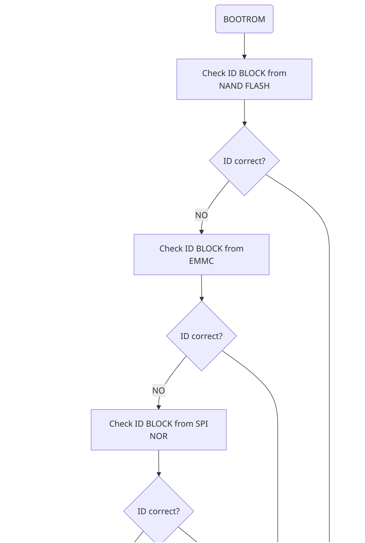
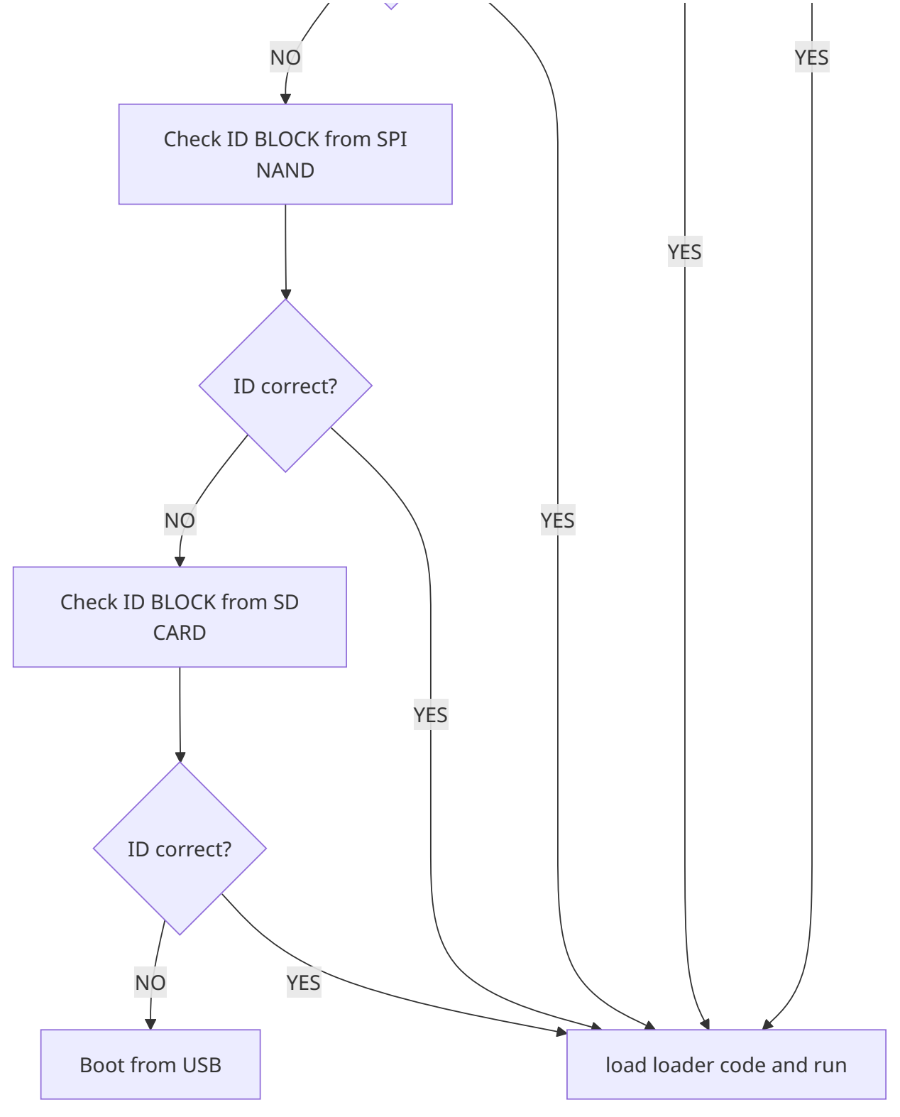
After an RK chip powers on, the first executed code is immutable mask code integrated into the chip: BOOTROM. Both AP and MCU integrate it. BOOTROM runs first, detects peripheral storage and loads its Loader code. Probe order differs by chip. The following flowchart is one BOOTROM boot example:
4.3 BOOTROM flow: original English source, page 28
4.3 BOOTROM flow: original English source, page 29
Notes:
- Some chips use different ADC-key input levels to select which storage BOOTROM probes. If that probe fails, the device enters maskrom mode directly.
- Storage detection normally reads a device ID to confirm an external device is present.
- If no valid firmware is detected on any device, maskrom mode waits for firmware download over a designated interface such as USB/UART. Not every chip supports USB/UART upgrading.
BOOTROM boot order for each chip
| AP | No.1 | No.2 | No.3 | No.4 | No.5 | No.6 |
|---|---|---|---|---|---|---|
| RK3188 | SD0 | NAND | SPI NOR(SPI0) | SPI NAND(SPI0) | EMMC | USB |
| RK3128 | NAND | EMMC | SPI NOR(SFC) | SPI NAND(SFC) | SD0 | USB |
| RK3126(B) | NAND | EMMC | SPI NOR(SFC) | SPI NAND(SFC) | SD0 | USB |
| RK3036 | NAND | EMMC | SPI NOR(SFC) | SPI NAND(SFC) | SD0 | USB |
| RK3288 | NAND | EMMC | SPI NOR(SPI2) | SPI NAND(SPI2) | SD0 | USB |
| RK3399 | SPI NOR(SPI2) | SPI NAND(SPI2) | EMMC | SD0 | USB | – |
| RK3368 | NAND | EMMC | SPI NOR(SFC) | SPI NAND(SFC) | SD0 | USB |
| RK3228/9 | NAND | EMMC | SPI NOR(SPI2) | SPI NAND(SPI2) | SD0 | USB |
| RK3328 | EMMC | SPI NOR(SPI2) | SPI NAND(SPI2) | SD0 | USB | – |
| RK3228H | EMMC | SPI NOR(SPI2) | SPI NAND(SPI2) | SD0 | USB | – |
| RK3128X/H | NAND | EMMC | SPI NOR(SPI2) | SPI NAND(SPI2) | SD0 | USB |
| RV1107/8 | NAND | EMMC | SPI NOR(SFC) | SPI NAND(SFC) | SD0 | USB |
| RV1109 | SPI NOR(SFC) | SPI NAND(SFC) | NAND | EMMC | SD0 | USB |
| RV1126 | SPI NOR(SFC) | SPI NAND(SFC) | NAND | EMMC | SD0 | USB |
| RK3308 | NAND | EMMC | SPI NOR(SFC) | SPI NAND(SFC) | SD0 | USB |
| RK3326 | NAND | EMMC | SPI NOR(SFC) | SPI NAND(SFC) | SD0 | USB |
| RKPX3 | SD0 | NAND | SPI NOR(SPI0) | SPI NAND(SPI0) | EMMC | USB |
| RKPX3SE | NAND | EMMC | SPI NOR(SFC) | SPI NAND(SFC) | SD0 | USB |
| RKPX5 | NAND | EMMC | SPI NOR(SFC) | SPI NAND(SFC) | SD0 | USB |
| RKPX30 | NAND | EMMC | SPI NOR(SFC) | SPI NAND(SFC) | SD0 | USB |
| RK1608 | SPI SLAVE | SPI NOR(SPI2) | SPI NAND(SPI2) | – | – | – |
| RK1808 | SPI SLAVE | SPI NOR(SFC) | SPI NAND(SFC) | EMMC | USB | – |
| RK3399PRO | SPI NOR(SPI2) | SPI NAND(SPI2) | EMMC | SD0 | USB | – |
| RK3568 | SPI NOR(SFC) | SPI NAND(SFC) | NAND | EMMC | SD0 | USB |
| RK3566 | SPI NOR(SFC) | SPI NAND(SFC) | NAND | EMMC | SD0 | USB |
| RK3588 | SPI NOR(SFC) | SPI NAND(SFC) | EMMC– | SD0 | USB | |
| RV1106/RV1103 | SPI NOR(SFC) | SPI NAND(SFC) | EMMC– | SD0 | USB/UART | |
| RK3528 | SPI NOR(SFC) | SPI NAND(SFC) | EMMC– | SD0 | USB | |
| RK3562 | SPI NOR(SFC) | SPI NAND(SFC) | EMMC– | SD0 | USB |
4.4 Pre Loader flow
An RK SDK build normally produces a MiniloaderAll.bin image. It has two principal functions: guiding firmware burning and burning the IDB image. The IDB image is the effective image unpacked from MiniloaderAll.bin, also called idblock, and is ultimately written to flash. It normally packages ddr.bin with a Pre Loader image; some chips support additional functional images. There are currently three main Pre Loader types in the source: closed-source miniloader, U-Boot SPL and loader.
4.4.1 Miniloader
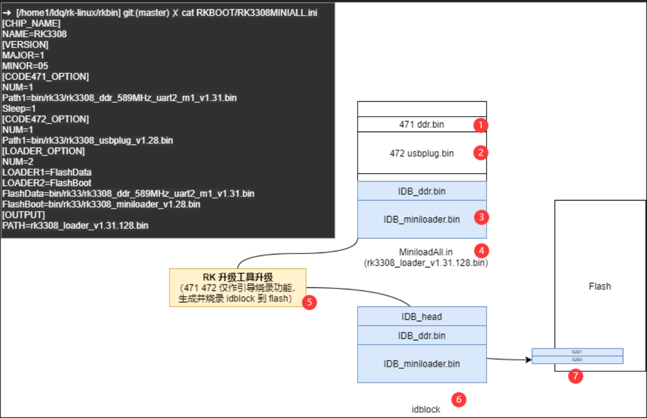
Introduction: miniloader is RK closed-source Pre Loader firmware, normally packaged with ddr.bin and usbplug.bin as loader.bin, with the following structure:
4.4.1 Miniloader: original English source, page 31
Comments:
1. ddr.bin: DDR initialization firmware, abbreviated 471.
2. usbplug.bin: runtime firmware for guiding firmware burning, abbreviated 472.
3. miniloader.bin: closed-source Pre Loader firmware.
4. MiniloaderAll.bin: SDK-wide standard filename, actually the packaged loader.bin for the corresponding chip.
5. During upgrading, RK tools extract idblock.bin from loader.bin, update it and maintain multiple backups.
6. idblock packages ddr.bin with Pre Loader; in the closed-source variant, Pre Loader means miniloader.bin.
Package Miniloader using the rkbin repository. For RK3308, enter the SDK rkbin directory and generate rk3308_loader_v1.xx.1xx.bin:
./tools/boot_merger ./RKBOOT/RK3308MINIALL.ini .
./tools/boot_merger ./RKBOOT/RK3308MINIALL_WO_FTL.ini . /* 尾缀为 _WO_FTL ⽂件、为开源存储⽅案选
⽤的 Pre Loader,⽂件系统选择ubifs或者jaffs2 */
./tools/boot_merger ./RKBOOT/RK3326MINIALL_SLC.ini . /* 尾缀为 _SLC ⽂件、为⼩容量存储(SLC
Nand、SPI Nand、SPI Nor)⽅案专⽤的 Pre Loader,内带rk ftl算法,不⽀持ubifs */
Like BOOTROM, Pre Loader probes different storage peripherals to support different storage types:

4.4.1 Miniloader: original English source, page 32
Because the code is closed source, users cannot change the boot order themselves.
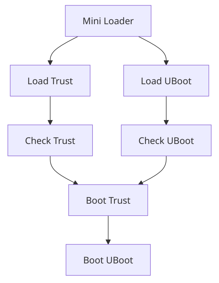
Boot flow:
4.4.1 Miniloader: original English source, page 33
4.4.2 u-boot spl
For chip support, see Rockchip-Developer-Guide-UBoot-nextdev-CN. NAND and SPI NAND support uses only open-source NAND drivers without FTL; UBIFS is recommended.
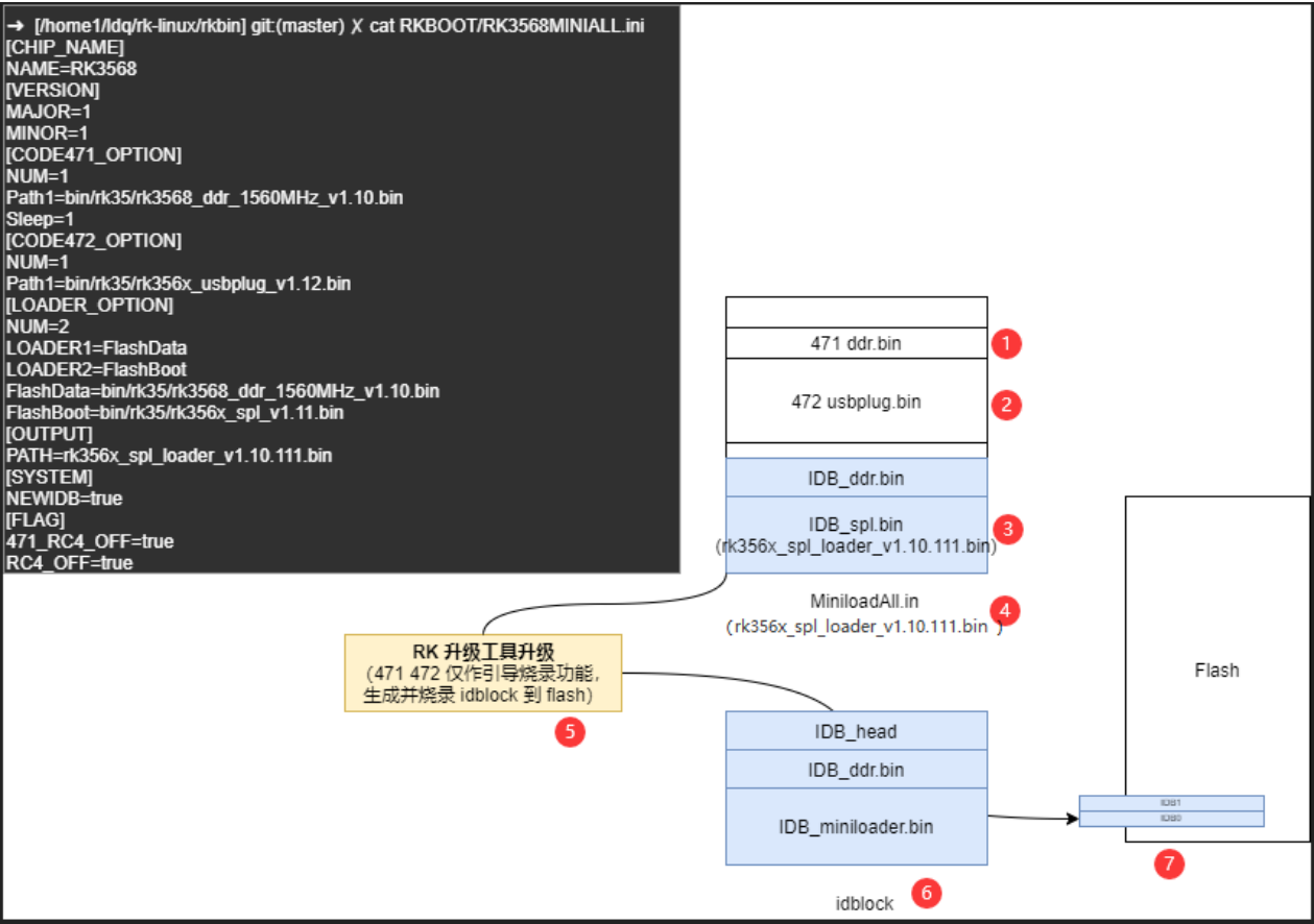
Introduction:
4.4.2 u-boot spl: original English source, page 34
Comments:
1. ddr.bin: DDR initialization firmware, abbreviated 471.
2. usbplug.bin: runtime firmware for guiding firmware burning, abbreviated 472.
3. spl.bin: SPL firmware built from U-Boot source, output as spl/u-boot-spl.bin under the U-Boot directory.
4. MiniloaderAll.bin: the SDK standard filename, actually the corresponding chip-specific spl_loader.bin package.
5. During upgrading, RK tools extract idblock.bin from loader.bin, update it and maintain multiple backups.
6. idblock packages ddr.bin with Pre Loader. In the SPL variant, Pre Loader is u-boot-spl.bin. RK SDK periodically builds u-boot-spl.bin and stores it in the corresponding rkbin directory as rkxxxx_spl_vx.xx.bin.
7. The PC upgrade tool maintains two idblock image copies for SLC NAND/SPI flash and five copies for other storage.
With the BOOTROM process in mind, interpret “load xxx.bin and run xxx function” as follows. Firmware burning:
- BOOTROM loads ddr.bin to initialize DDR.
- BOOTROM loads usbplug.bin and uses the USB plug firmware for burning.
Startup:
- BOOTROM loads ddr.bin to initialize DDR.
- BOOTROM loads spl.bin to perform Loader functions and load subsequent firmware.
Some chips also package mcu.bin and PCIe.bin in idblock with similar behavior and purpose: pre-load the pre-loader.
SPL storage probe order:

4.4.2 u-boot spl: original English source, page 35
Notes:
- SPL can enable SD-card boot: when a card with valid firmware is found, subsequent firmware is loaded from it to complete SD startup.
- SPL firmware supporting atags prioritizes the storage successfully detected by BOOTROM; see the U-Boot developer guide for atags details.
SPL storage-related log:
U-Boot SPL 2017.09-gcc781e0266-230509-dirty #ldq (Nov 24 2023 - 00:15:39)
unknown raw ID 0 0 0
unrecognized JEDEC id bytes: 00, 00, 00
Trying to boot from MMC2
MMC: no card present
mmc_init: -123, time 0
spl: mmc init failed with error: -123
Trying to boot from MMC1                # bootdev 探测结果:MMC2(SD Card)、MMC1(EMMC)、
MTD0(SLC Nand)、MTD1(SPI Nand)、MTD2(SPI Nor)
No misc partition
Trying fit image at 0x4000 sector
Boot flow:
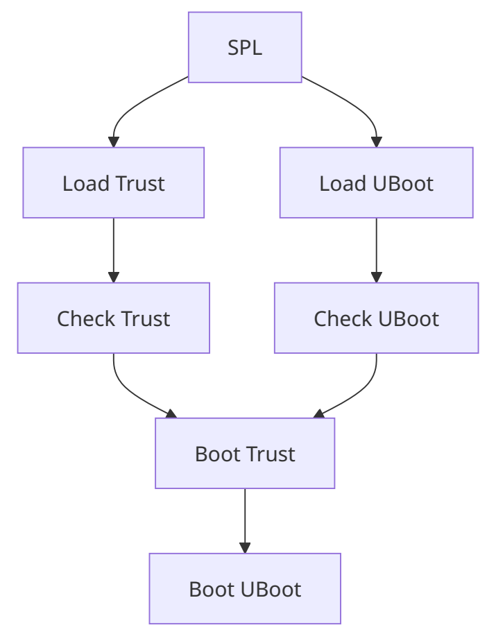
4.4.2 u-boot spl: original English source, page 36
English-source addition: pages 36–37 contain an extra Loader probe-order and boot-flow pair after the SPL text, repeated in the later Loader section. The Chinese source has no figures at that position. They are retained below in source order; their placement does not establish that they describe a distinct SPL-only flow.

4.4.2 u-boot spl: original English source, page 36
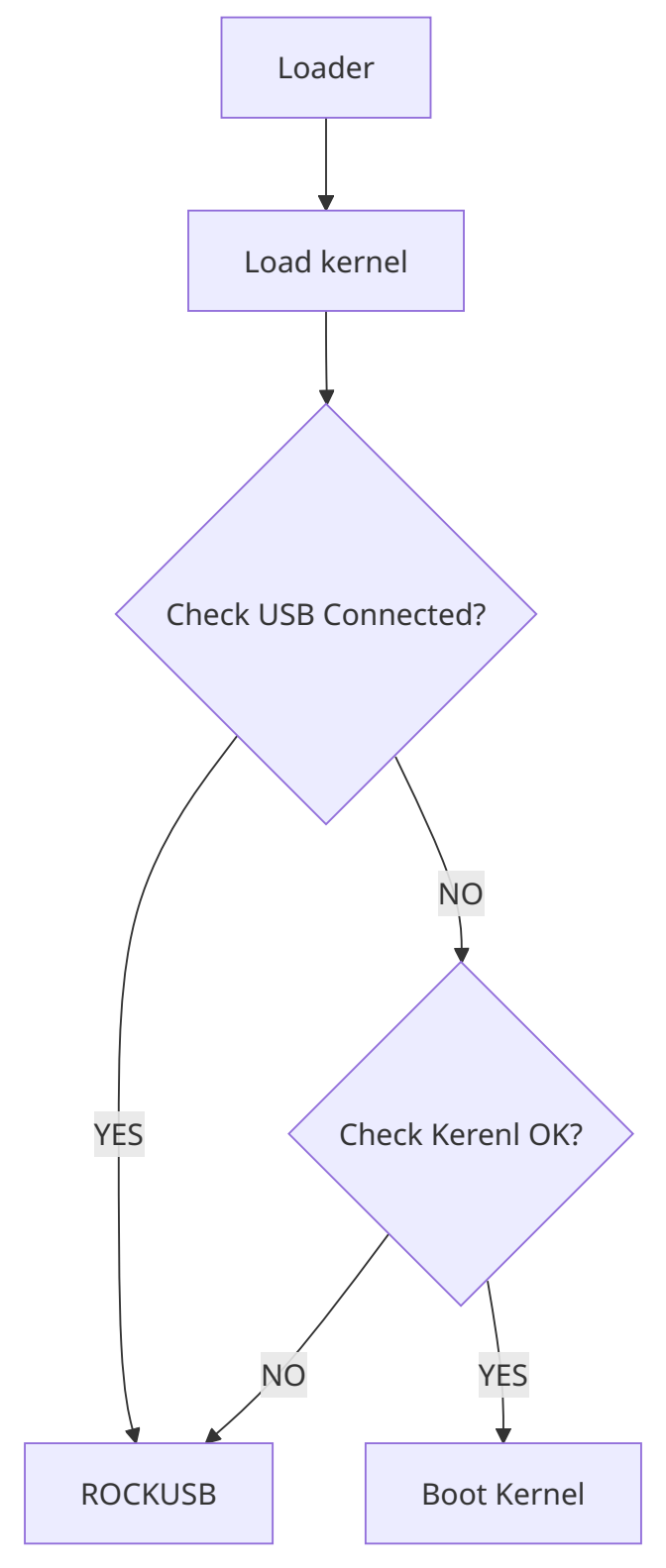
4.4.2 u-boot spl: original English source, page 37
4.4.3 loader
Supported platforms include RV1107, RV1108, RK3036, RK3128 and RK3229. This loader generally serves small-capacity storage and boots the kernel directly without U-Boot.
| Chip | SD CARD | SLC NAND | EMMC | SPI NOR | SPI NAND |
|---|---|---|---|---|---|
| RV1107/8 | Supported | Supported | Supported | Supported | Supported |
| RK3036 | Supported | Supported*1 | Supported*1 | Supported | Supported |
| RK3128 | Supported | Supported*1 | Supported*1 | Supported | Supported |
| RK3229 | Supported | Supported*1 | Supported*1 | Supported | Not supported |
*1: RK3036, RK3128 and RK3229 projects using SLC NAND or EMMC generally use miniloader directly.
Storage probe order:

4.4.3 loader: original English source, page 38
Boot flow:
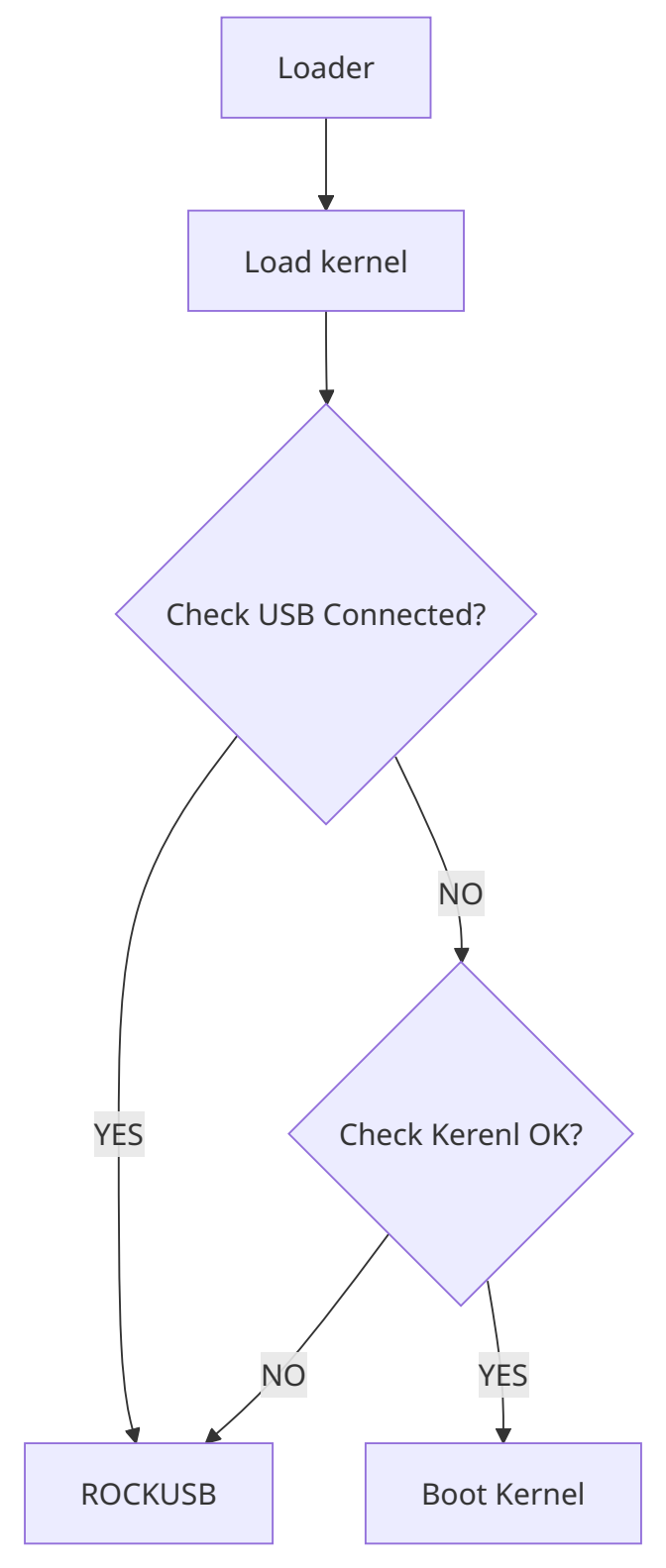
4.4.3 loader: original English source, page 39
5. Partitions and data storage
5.1 Data storage
5.1.1 Introduction to address translation
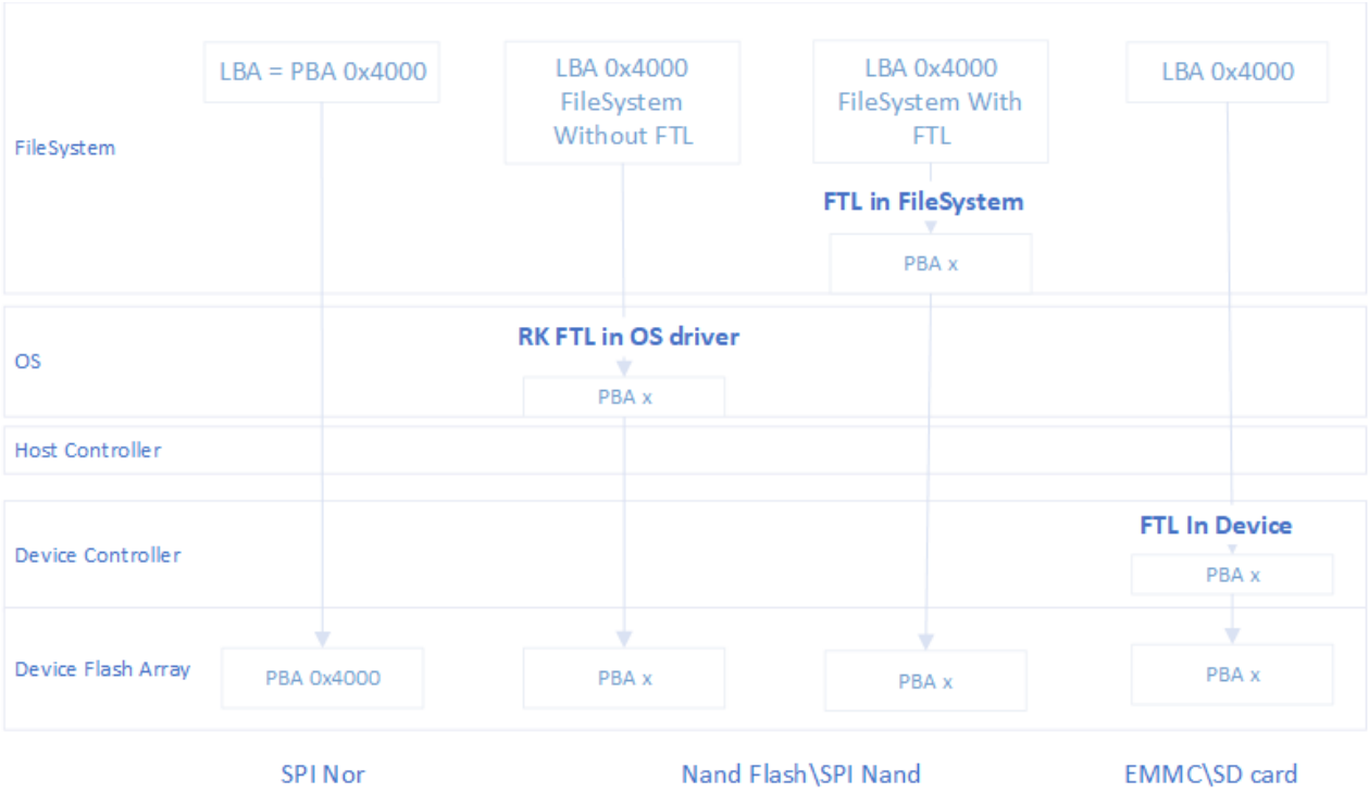
Most storage devices are not flat-mapped: a user logical sector address (LBA) is translated into a flash physical sector address (PBA). This mapping is FTL (Flash Translation Layer), which accounts for wear, bad blocks and garbage collection. With or without FTL, users and files need consider only logical addresses; software handles translation. For an access to sector address 0x4000, the relationship is:
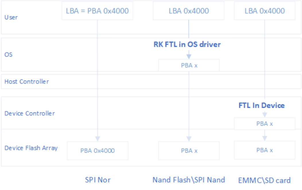
5.1.1 Introduction to address translation: original English source, page 40
For a filesystem-interface access to sector address 0x4000, address translation is:
5.1.1 Introduction to address translation: original English source, page 41
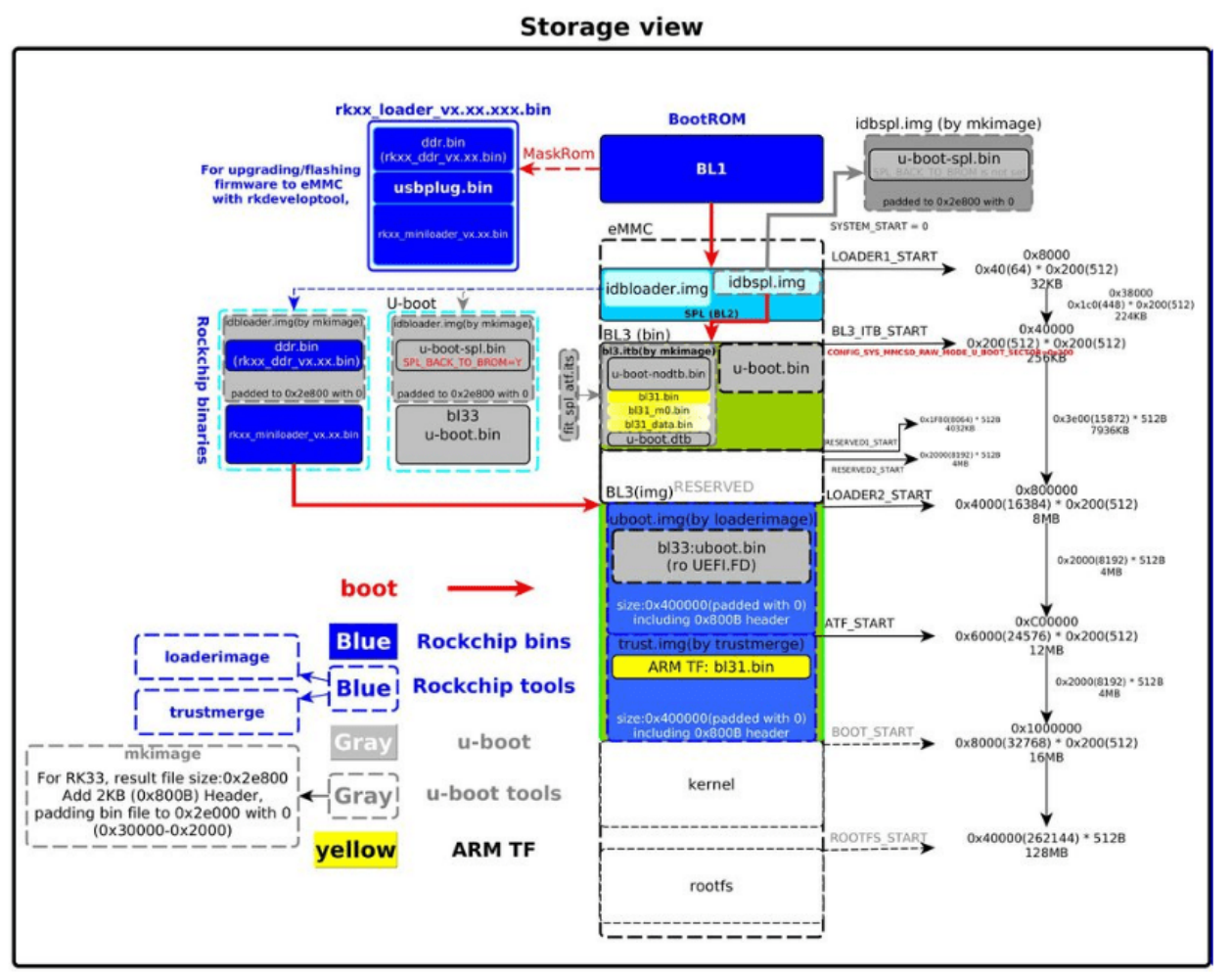
5.1.2 Partitions and logical data addresses
5.1.2 Partitions and logical data addresses: original English source, page 42
5.2 Partition-table layouts
RK storage solutions have three partition-table types that can be stored in a storage partition: MTD Partition, GPT and RK partition. See Rockchip_Introduction_Partition for details.
| Partition | Description | Applicable platforms | Restrictions |
|---|---|---|---|
| MTD Partition |
Defined in parameter and passed through cmdline; no longer supported starting with uboot-next | All APs*1 | Requires a separate partition |
| GPT | EFI GUID partition table; supported by uboot-next | All APs*2 | Uses somewhat more resources |
| RK partition | Based on GPT; primarily for small-capacity storage to save resources | RV1107/8, MCU |
RK-specific, not universal |
*1: platforms on the uboot-next branch no longer support MTD partition; adaptation is required if it is needed.
*2: uboot-next platforms use GPT by default; other table types require adaptation.
5.2.1 MTD Partition
See Rockchip_Developer_Guide_Linux_Flash_Open_Source_Solution_CN.md.
5.2.2 GPT
GPT is configured through a parameter file, with a structure similar to MTD Partition. Four differences are:
1. Set TYPE to GPT.
2. Do not define a parameter partition; even if defined, it is not used.
3. Add the keyword grow to the last partition.
4. Specify the rootfs UUID; SDK defaults may differ, and it must match the rootfs UUID defined in DTS.
FIRMWARE_VER:8.1
MACHINE_MODEL:RK3326
MACHINE_ID:007
MANUFACTURER: RK3326
MAGIC: 0x5041524B
ATAG: 0x00200800
MACHINE: 3326
CHECK_MASK: 0x80
PWR_HLD: 0,0,A,0,1
TYPE: GPT /* GPT 分区 */
CMDLINE:mtdparts=rk29xxnand:0x00002000@0x00004000 (uboot),0x00002000@0x00006000(trust),0x00002000@0x00008000 (misc),0x00008000@0x0000a000 (resource),0x00010000@0x00012000(kernel),0x00010000@0x00022000 (boot),0x00020000@0x00032000 (recovery),0x00038000@0x00052000(backup),0x00002000@0x0008a000 (security),0x000c0000@0x0008c000(cache),0x00300000@0x0014c000 (system),0x00008000@0x0044c000(metadata),0x000c0000@0x00454000 (vendor),0x00040000@0x00514000 (oem),0x00000400@0x00554000(frp),-@0x00554400 (userdata:grow)
uuid:rootfs=614e0000-0000-4b53-8000-1d28000054a9
GPT upgrade procedure:
1. The tool reads partition definitions from parameter.
2. It obtains storage capacity from the Loader.
3. It resizes the last partition and creates a GPT table file.
4. It writes the table at storage address 0 and address -33 at the tail.
Note 1: the parameter file itself is not written to storage.
5.2.3 RK partition
RK partition is a custom table with GPT-like structure, low resource use and faster initialization, mainly used on RV1107/8 and MCU platforms. The following is a Linux/Android product partition-definition template:
#Flag ⽬前只有两个值,1 为分区需要下载,0 为不需要下载
#type ⽬前有 5 种值,0x1=Vendor 分区 0x2=IDBlock 分区 0x4=Kernel 分区 0x8=boot 分区 0x80000000 = 普通分区

#PartSize 和 PartOffset 字段的值都是以扇区为单位
[System]
FwVersion=16.12.23
# 如果 Nano=1, 则⽣成 nano 的 idblock
Nano=
# 如果 BLANK_GAP=1, 则⽣成的 idblock 按每 2k 数据间隔 2k 空⽩保存
BLANK_GAP=1
#FILL_BYTE 表⽰分区尾部空⽩⽤什么数据填充,默认为 0
FILL_BYTE=
[IDBlock]
Flag=1
DDR_Bin=rk3399_DDR_800MHz_v1.17.bin
Loader_Bin=rk3399_miniloader_spi_nor_v1.14.bin
PartOffset=0x40
PartSize=0x780
[UserPart1]
Name=trust
Type=0x10
Flag=1
File=trust_1MB.img
PartOffset=0x800
PartSize=0x800
[UserPart2]
Name=uboot
Type=0x20
Flag=1
File=uboot_1MB.img
PartOffset=0x1000
PartSize=0x800
Normal partition
The following is the RTOS product template. The specification for bits [8,10] of Flag currently applies only to RTOS products in the source:
#Flag:
#  bits filed:
#  [0]    : skip                  : 0 - disabled (default), 1 - enable
#  [2]    : no partition size     : 0 - diabled (default), 1 - enable
#  [8, 9] : property              : 0 - do not register (default), 1 - read only, 2 - write only, 3 - rw
#  [10]   : register type         : 0 - block partition (default), 1 - MTD partition
#type can suppot 32 partiton types,0x0:undefined 0x1:Vendor 0x2:IDBlock ,bit3:bit31 are available
#PartSize and PartOffset unit by sector
#Gpt_Enable 1:compact gpt,0:normal gpt
#Backup_Partition_Enable 0:no backup,1:backup
#Loader_Encrypt 0:no encrypt,1:rc4
#nano 1:generate idblock in nano format
[System]
FwVersion=1.0
Gpt_Enable=
Backup_Partition_Enable=
Nano=
Loader_Encrypt=
Chip=
Model=
[UserPart1]
Name=IDBlock
Type=0x2
PartOffset=0x80
PartSize=0x80
Flag=
File=../../Image/rk2108_loader.bin,../../Image/Boot2_Fake.bin
[UserPart2]
Name=rtthread
Type=0x8
PartOffset=0x100
PartSize=0xa00
Flag=
File=../../Image/rtthread.img
[UserPart3]
Name=root
Type=
PartOffset=0x1100
PartSize=0x6f00
Flag=0x305
File=../../Image/root.img
5.2.4 ENV partitions
ENV (Environment-Variables) is a U-Boot mechanism for global data management and transfer. A hash table manages user data as key–data entries. Some RK platforms store ENV in flash as an ENV partition, generate mtdparts partition information from cmdlines and record it in the ENV table, then pass it from SPL or U-Boot to the kernel.
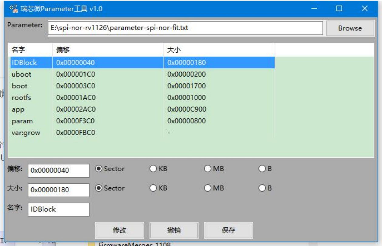
5.3 parameter partition-table editing tool
The partition-table modification tool edits partitions defined in parameter. Resizing a partition also adjusts the offsets of all following partitions.
5.3 parameter partition-table editing tool: original English source, page 47
5.4 Partition write protection
5.4.1 Write protection for block-device partitions
EMMC and SD CARD are block devices in the Linux kernel. NAND FLASH is also a block device when using rknand or rkflash. The following commands configure partition access properties. Example 1: make the system partition read-only:
./busybox blockdev --setro /dev/block/by-name/system
Example 2: make system readable and writable:
./busybox blockdev --setrw /dev/block/by-name/system
Note: configure the partition before mounting it. If a partition is mounted writable and then changed to read-only, the filesystem reports errors.
5.4.2 Write protection for MTD partitions
MTD partitions are normally defined through cmdline. Append ro to the partition name to mark it read-only. To protect a specific partition, modify mtdparts when U-Boot passes cmdline to the kernel. Example: change the partition table to make boot read-only:
mtdparts=rk29xxnand:0x00002000@0x00004000(uboot),0x00004000@0x00006000(boot)ro,...
6. Firmware programming
There are three main methods for programming firmware in production: USB upgrade, SD-card upgrade, and programming with a dedicated programmer.
6.1 USB upgrade
USB upgrades use two protocols: rockusb and fastboot. This document describes only rockusb; for fastboot, see Rockchip-Developer-Guide-UBoot-nextdev-CN.
6.1.1 Flow diagram

6.1.1 Flow diagram: original English source, page 49
AP rockusb: maskrom rockusb, miniloader rockusb and uboot rockusb. NVM: SPI NOR, SPI NAND, SLC NAND, EMMC, M/TLC NAND.
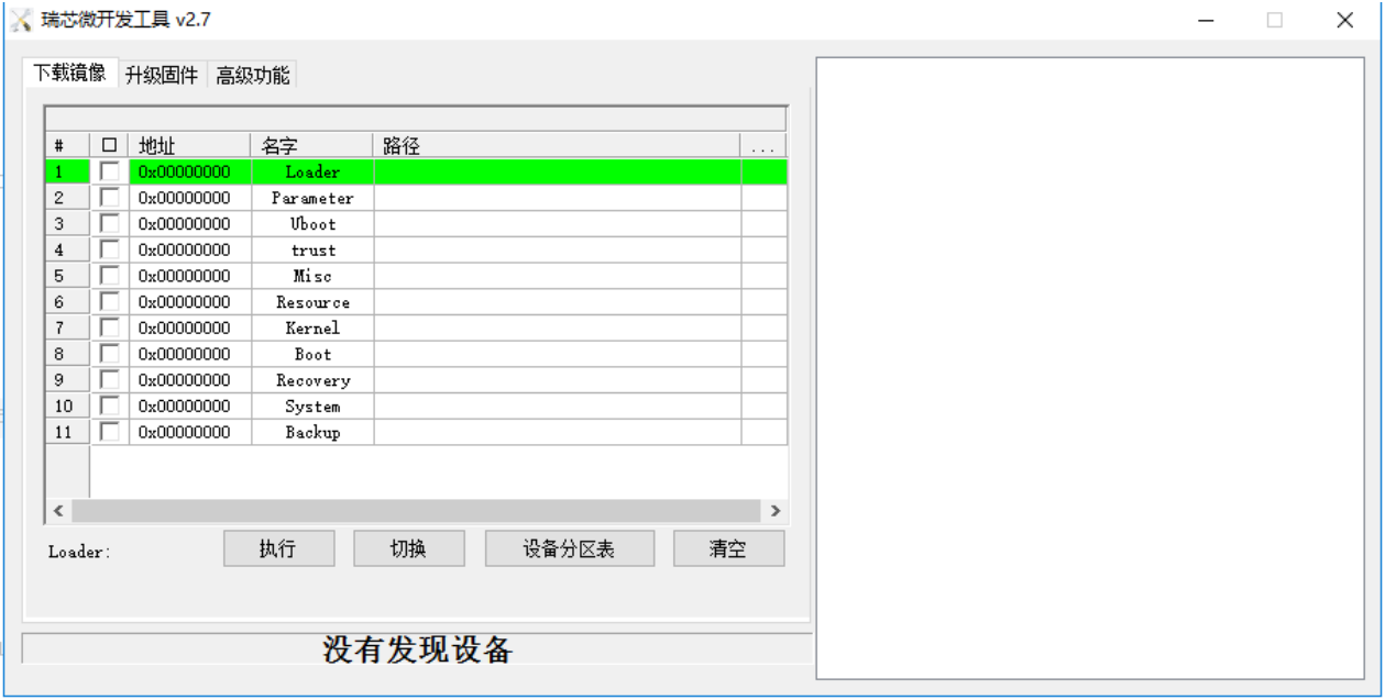
6.1.2 Windows: RKDevTool
For GPT/RKPartition layouts, the AP SDK provides development tools for configuring and upgrading either complete firmware or individual partitions. See the accompanying tool documentation for details. Some useful functions are listed below:
1. Read the device partition table: in Loader upgrade mode, click “Device Partition Table”.
2. In MSC/MTP mode, click “Switch” to enter Loader mode.
3. In Advanced Functions, use “Enter maskrom” to switch from Loader to maskrom.
4. In Loader or maskrom mode, use “Restart Device”. Tool interface:
6.1.2 Windows: RKDevTool: original English source, page 50
Advanced functions:
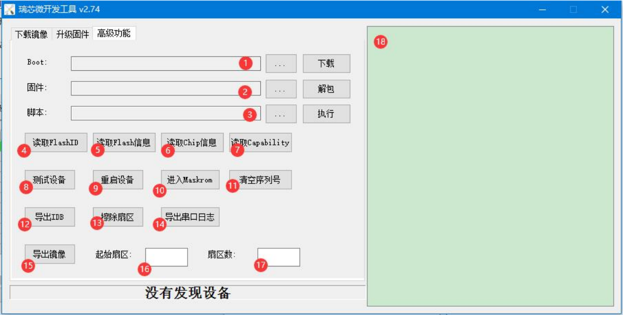
6.1.2 Windows: RKDevTool: original English source, page 50
1. In maskrom mode, select and download a Loader to run in DDR.
2. Unpack update.img.
3. Run a script.
4. Read the FLASH ID.
5. Read FLASH information.
6. Read chip information.
7. Read the extended functions supported by the Loader.
8. Test whether the device is ready.
9. Restart the device.
10. Restart into maskrom, normally switching from Loader to maskrom.
11. Overwrite data to clear the serial number. This operation may damage the firmware.
12. Export the IDB structure in the Loader header.
13. Erase using the start address and sector count from fields 16 and 17. The range must be aligned to 4 MB; otherwise, more or less data may be erased than intended.
14. Export Loader runtime serial-port information to the tool output directory.
15. Export a firmware image to the tool output directory using the start address and sector count from fields 16 and 17.
16. Define the starting sector.
17. Define the number of sectors to operate on.
18. Tool log.
6.1.3 Windows: SocToolKit
Some APs support the open-source ENV partition-information scheme. The partition table and bootargs are written to ENV and passed to the kernel through cmdline. Dedicated image-packaging and upgrade tools are provided. Tool interface:
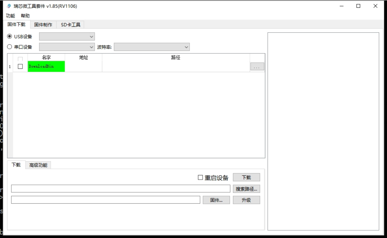
6.1.3 Windows: SocToolKit: original English source, page 51
6.1.4 Linux: upgrade_tool
The Linux tool provides functions similar to the Android tool. Tool interface:
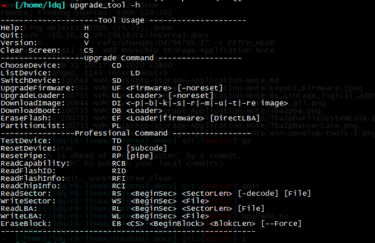
6.1.4 Linux: upgrade_tool: original English source, page 52
6.1.5 Linux: SocToolKit
The Linux tool provides functions similar to the Android tool.
6.1.6 Production tool
The production tool supports asynchronous programming of multiple devices. Once the upgrade operation is running, each connected device is upgraded independently. Tool interface:
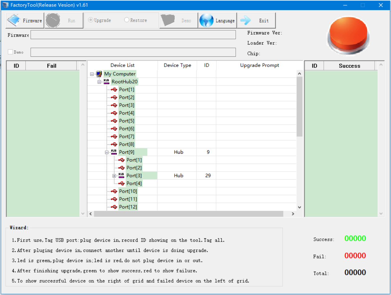
6.1.6 Production tool: original English source, page 53
Each option in config.ini has a detailed comment. Common configuration options:
1. FW_BURN_EFUSE: write efuse while programming firmware to enable secure boot. This cannot be enabled if the AP uses OTP or the PCB has no EFUSE power-supply control.
2. NOTRESET_AFTER_UPGRADE: do not restart after upgrading. This is required for products that must not lose power during their first startup.
3. FORCE_DATA_BAND: change the USB packet size. Reduce it if SPI NOR USB transfers time out.
4. SN_DLL_ON: write the serial number during the upgrade.
5. RB_CHECK_OFF: controls whether firmware upgrades require read-back verification. The original describes the function without defining the flag polarity here.
6.2 SD-card upgrade
SD_Firmware_Tool writes update.img to an SD upgrade card. Insert it into the SD/TF slot and power on: the device starts from SD, enters recovery, and upgrades internal storage. Tool interface:
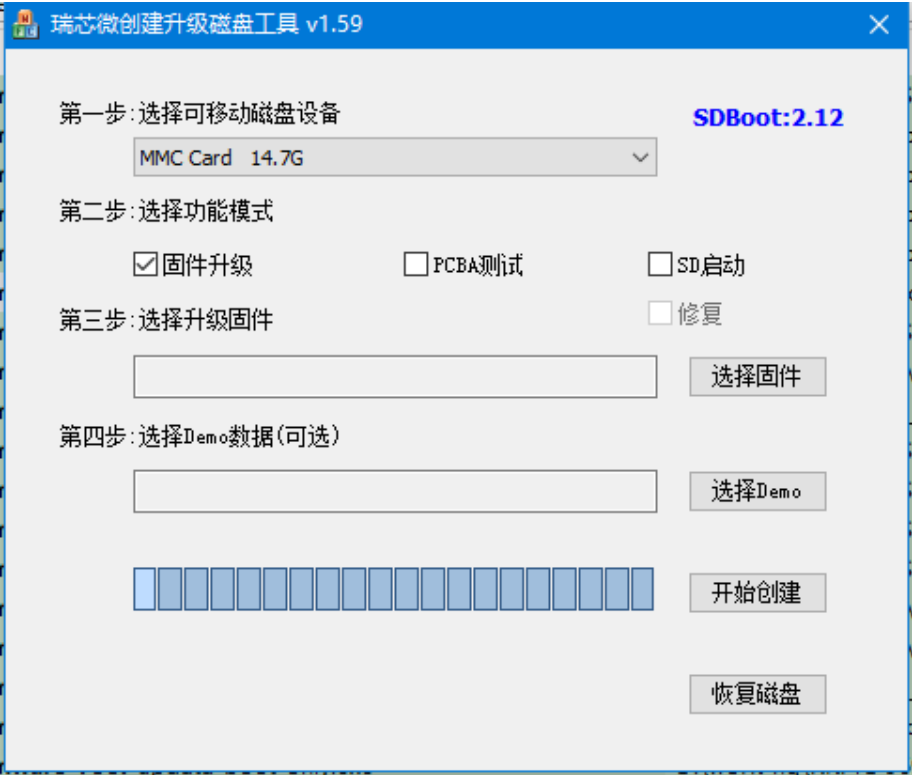
6.2 SD-card upgrade: original English source, page 54
Tool functions:
1. PCBA test: perform the test before upgrading.
2. SD boot: create a boot card containing the complete firmware.
3. Restore disk: remove the boot code and restore the card for ordinary SD-card use.
6.3 UART upgrade
UART upgrades on supported chips are available in the Linux, Windows and production tools.
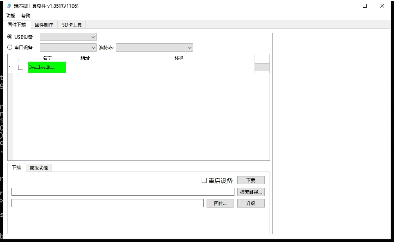
6.3 UART upgrade: original English source, page 55
6.4 EMMC image programming
SpiImageTools converts update.img into an image for a dedicated programmer. Tool interface:
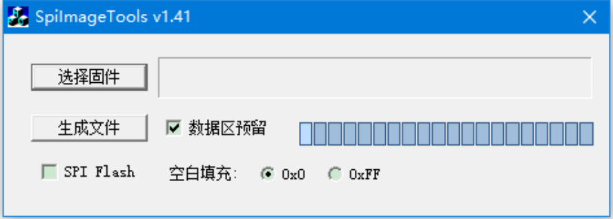
6.4 EMMC image programming: original English source, page 55
Tool configuration:
1. Blank-area fill: select 0x0 for EMMC.
2. Do not select SPI FLASH.
3. Enable data-area reservation. To create an image for GPT firmware, parameter must contain DISKSIZE; see Rockchip Production Programming Guide_v1.2. Programmer settings:
1. Write data.bin to the EMMC user partition.
2. For RK3188/RKPX3, write boot0.bin to both EMMC boot1 and boot2.
3. Enable skipping all-zero data in the programmer.
4. Leave all CSD values at their defaults.
5. Leave unlisted EXTCSD entries at their defaults.
RK3188/RKPX3:
- EXT_CSD[167] = 0x1f (must be set if supported by the device).
- EXT_CSD[162] = 0x1: enable the reset pin.
- EXT_CSD[177] = 0x0 (default).
- EXT_CSD[178] = 0x0 (default).
- EXT_CSD[179] = 0x8: boot from boot1.
Other APs:
- EXT_CSD[167] = 0x1f (must be configured if supported).
- EXT_CSD[162], EXT_CSD[177], EXT_CSD[178] and EXT_CSD[179] = 0x0 (default).
6.5 SLC NAND image programming
See the corresponding section of Rockchip_Developer_Guide_Linux_Nand_Flash_Open_Source_Solution_CN.pdf.
6.6 SPI NAND image programming
See the corresponding section of Rockchip_Developer_Guide_Linux_Nand_Flash_Open_Source_Solution_CN.pdf.
6.7 SPI NOR image programming
See the corresponding section of Rockchip_Developer_Guide_Linux_Nand_Flash_Open_Source_Solution_CN.pdf.
7. Storage software-driver configuration
Rockchip mainly provides the following storage solutions:
| Solution | Main supported device types | Main supported filesystems | Programming methods |
|---|---|---|---|
| eMMC solution | eMMC | FAT、EXT、 SquashFS |
USB upgrade, SD-card upgrade |
| rknand solution | MLC、TLC Nand | FAT、EXT、 SquashFS |
USB upgrade, SD-card upgrade |
| rkflash solution | SLC Nand、SPI Nand |
FAT、EXT、 SquashFS |
USB upgrade, SD-card upgrade |
| rkflash solution (SPI NOR support) | SPI Nor | SquashFS、JFFS2 | USB upgrade, SD-card upgrade, programmer |
| SLC Nand open-source solution | SLC Nand | UBIFS | USB upgrade, SD-card upgrade, programmer |
| SPI Nand open-source solution | SPI Nand | UBIFS | USB upgrade, SD-card upgrade, programmer |
| SPI Nor open-source solution | SPI Nor | SquashFS、JFFS2 | USB upgrade, SD-card upgrade, programmer |
7.1 u-boot
For U-Boot details, see CH05 Driver Modules / Storage in Rockchip-Developer-Guide-UBoot-nextdev-CN.
7.2 kernel
In kernel 4.4 and earlier, open-source SPI flash support is incomplete. The kernel open-source flash solution differs from that of U-Boot.
| Solution | Main supported device types | Host-controller driver | Flash framework | Registered device type | Main supported filesystems | Programming methods |
|---|---|---|---|---|---|---|
| rknand solution | MLC TLC Nand |
drivers/rkand | drivers/rkand | Block device | FAT、EXT、 SquashFS |
USB upgrade, SD-card upgrade |
| rkflash solution | SLC Nand、 SPI Nand |
drivers/rkflash | drivers/rkflash | Block device | FAT、EXT、 SquashFS |
USB upgrade, SD-card upgrade |
| rkflash solution (SPI NOR support) | SPI Nor | drivers/rkflash | drivers/rkflash | Block or MTD device | SquashFS、 JFFS2 |
USB upgrade, SD-card upgrade, programmer |
| SLC Nand open-source solution | SLC Nand | drivers/mtd/ nand/raw |
drivers/mtd/ nand/raw |
mtd | UBIFS | USB upgrade, SD-card upgrade, programmer |
| SPI Nand open-source solution | SPI Nand | drivers/rkflash | drivers/rkflash | mtd | UBIFS | USB upgrade, SD-card upgrade, programmer |
| SPI Nor open-source solution | SPI Nor | drivers/rkflash | drivers/rkflash | MTD or MTD block device | SquashFS、 JFFS2 |
USB upgrade, SD-card upgrade, programmer |
7.2.1 MLC NAND/TLC NAND: rknand solution
Configuration:
CONFIG_RK_NAND=y
Driver files:
./drivers/rk_nand/
7.2.2 SLC NAND/SPI NAND/SPI NOR: rkflash solution
See Rockchip_Developer_Guide_Linux_Flash_Open_Source_Solution_CN.md.
7.2.3 SLC NAND/SPI NAND/SPI NOR: open-source MTD solution
See Rockchip_Developer_Guide_Linux_Flash_Open_Source_Solution_CN.md.
7.3 Storage iomux/clk configuration and scan order at each stage
| Stage | Storage device | iomux configuration | Clock configuration | Driver configuration |
|---|---|---|---|---|
| maskrom | Scan nor, spinand, emmc, sdcard | Configured only for a successfully detected device | Configured | |
| spl | Priority 1 (atags supported): device detected by maskrom. Priority 2: scan nor, spinand, emmc, sdcard. |
1. Not configured (default). 2. Supplement the required iommux configuration. |
Configured in driver | Configure dts/defconfig for the specific SDK |
| uboot | Priority 1 (disabled by default): target specified by CONFIG_ROCKCHIP_BOOTDEV. Priority 2 (atags supported): device detected by maskrom. Priority 3: scan nor, spinand, emmc, sdcard. |
Not configured | Configured in driver | Configure dts/defconfig for the specific SDK |
| kernel | Scan nor, spinand, emmc, sdcard | Configure dts/defconfig for the specific SDK |
7.4 Dual-storage extension
See Rockchip_Developer_Guide_Dual_Storage_CN.md.
8. OTA for open-source solutions
See Rockchip_Developer_Guide_Linux_Flash_Open_Source_Solution_CN.md.
9. Filesystem support
9.1 UBIFS filesystem
See Rockchip_Developer_Guide_Linux_Flash_Open_Source_Solution_CN.md.
9.2 JFFS2 filesystem support
See Rockchip_Developer_Guide_Linux_Flash_Open_Source_Solution_CN.md.
10. Using Vendor Storage
Vendor Storage stores small non-security data such as serial numbers and MAC addresses. References:
- EMMC: Rockchip_Application_Notes_VendorStorage.
- Flash using rkflash: Rockchip_Application_Notes_VendorStorage.
- Flash using MTD: Rockchip_Developer_Guide_Linux_Flash_Open_Source_Solution_CN.pdf.
10.1 Vendor Storage ID
A Vendor ID is 16 bits wide and identifies data independently of its storage location, like an index or filename. IDs 0–31 are reserved for common SDK functions; customers may use 32–65535. ID functions are listed below:
| ID | Function |
|---|---|
| 0 | reserved |
| 1 | SN |
| 2 | WIFI MAC |
| 3 | LAN MAC |
| 4 | BT MAC |
| 5 | HDCP 1.4 HDMI |
| 6 | HDCP 1.4 DP |
| 7 | HDCP 2.X |
| 8 | DRM KEY |
| 9 | PLAYREADY Cert |
| 10 | ATTENTION KEY |
| 11 | PLAYREADY ROOT KEY 0 |
| 12 | PLAYREADY ROOT KEY 1 |
| 13 | SENSOR CALIBRATION |
| 14 | RK reserved for future use |
| 15 | IMEI |
| 16 | LAN_RGMII_DL |
| 17 – 31 | RK reserved for future use |
| 32 - 65535 | Vendor use |
10.2 Vendor Storage API
10.2.1 Uboot API
int vendor_storage_init (void)
    function: Initialize vendor storage
    input: none
    return: 0, Initialize success
            other, Initialize fail
int vendor_storage_read (u32 id, void *pbuf, u32 size)
    function: read vendor storage by id
    input: id, item id; pbuf, data buffer; size, number byte to read.
    return: -1, read fail.
            other: number byte have read.
int rk_vendor_write (u32 id, void *pbuf, u32 size)
    function: write vendor storage by id
    input: id, item id; pbuf: data buffer; size: number bytes to write.
    return: 0: write success
            other : write fail
10.2.2 kernel API
Source code: kernel/drivers/soc/rockchip/rk_vendor_storage.c
Include header: include/linux/soc/rockchip/rk_vendor_storage.h
int vendor_storage_init (void)
    function: Initialize vendor storage
    input: none
    return:  0, Initialize success
            other, Initialize fail
int vendor_storage_read (u32 id, void *pbuf, u32 size)
    function: read vendor storage by id
    input: id, item id; pbuf, data buffer; size, number byte to read.
    return: -1, read fail.
            other: number byte have read.
int rk_vendor_write (u32 id, void *pbuf, u32 size)
    function: write vendor storage by id
    input: id, item id; pbuf: data buffer; size: number bytes to write.
    return: 0: write success
            other : write fail
10.2.3 User API
A user application reads and writes through IOCTL. Reference code:
#include <fcntl.h>
#include <sys/ioctl.h>

#define VENDOR_REQ_TAG  0x56524551
#define VENDOR_READ_IO  _IOW ('v', 0x01, unsigned int)
#define VENDOR_WRITE_IO _IOW ('v', 0x02, unsigned int)
#define VENDOR_SN_ID        1
#define VENDOR_WIFI_MAC_ID  2
#define VENDOR_LAN_MAC_ID   3
#define VENDOR_BLUETOOTH_ID 4

struct rk_vendor_req {
    u32 tag;
    u16 id;
    u16 len;
    u8 data [1];
};

static void print_hex_data (uint8 *s, uint32 *buf, uint32 len)
{
    uint32 i, j, count;

    ERROR ("% s", s);
    for (i = 0; i < len; i += 4)
        ERROR ("% x % x % x % x", buf [i], buf [i + 1], buf [i + 2], buf [i + 3]);
}

int vendor_storage_read_test (void)
{
    u32 i;
    int ret, sys_fd;
    u8 p_buf [2048];/* malloc req buffer or used extern buffer */
    struct rk_vendor_req *req;

    req = (struct rk_vendor_req *) p_buf;
    sys_fd = open ("/dev/vendor_storage", O_RDWR, 0);
    if (sys_fd < 0){
        ERROR ("vendor_storage open fail\n");
        return -1;
    }

    req->tag = VENDOR_REQ_TAG;
    req->id = VENDOR_SN_ID;
    req->len = 512; /* max read length to read*/
    ret = ioctl (sys_fd, VENDOR_READ_IO, req);
    print_hex_data ("vendor read:", (uint32*) req, req->len + 8);
/* return req->len is the real data length stored in the NV-storage */
    if (ret){
        ERROR ("vendor read error\n");
        return -1;
    }

    return 0;
}

int vendor_storage_write_test (void)
{
    uint32 i;
    int ret, sys_fd;
    uint8 p_buf [2048]; /* malloc req buffer or used extern buffer */
    struct rk_vendor_req *req;

    req = (struct rk_vendor_req *) p_buf;
    sys_fd = open ("/dev/vendor_storage", O_RDWR, 0);
    if (sys_fd < 0){
        ERROR ("vendor_storage open fail\n");
        return -1;
    }

    req->tag = VENDOR_REQ_TAG;
    req->id = VENDOR_SN_ID;
    req->len = 32; /* data len */
    for (i = 0; i < 32; i++)
        req->data [i] = i;
    print_hex_data ("vendor write:", (uint32*) req, req->len + 8);
    ret = ioctl (sys_fd, VENDOR_WRITE_IO, req);
    if (ret){
        ERROR ("vendor write error\n");
        return -1;
    }

    return 0;
}
10.2.4 PC Tool API
The PC tool provides source code for a C++ reference project with two read/write APIs:
int RK_ReadProvisioningData (int id, (PBYTE) pbuf, int size)
    function: read vendor storage by id
    input: id, item id; pbuf, data buffer; size, number byte to read.
    return: 0, read data okay.
            other: read fail.
int  RK_WriteProvisioningData (int id, (PBYTE) pbuf, int size)
    function: write vendor storage by id
    input: id, item id; pbuf: data buffer; size: number bytes to write.
    return:  0: write success
            other : write fail
10.3 Usage notes
10.3.1 Maximum data size of one VENDOR item
The NAND/EMMC Vendor partition has a total size of 64 KB; NOR uses 4 KB. Data is stored in the vendor structure.
struct vendor_info {
    struct vendor_hdr *hdr; //32byte
    struct vendor_item *item; //8byte * item
    u8 *data; //size = sum (item 1, item 2, ... item n)
    u32 *hash;
    u32 *version2;
};
If only one item is written:
NAND/EMMC: a single data item can hold 64*1024-32-8-4-4 = 65488 bytes.
NOR: a single data item can hold 4*1024-32-8-4-4 = 4048 bytes.
10.3.2 Dual-copy support for VENDOR data
Two copies are maintained by default:
- If power fails while writing the first copy, retaining old data is unavoidable.
- If power fails while writing the second copy, the first copy is used.
11. Appendix references
Reference links:
- http://www.linux-mtd.infradead.org/faq/ubi.html
- http://www.linux-mtd.infradead.org/faq/ubifs.html#L_lebsz_mismatch
- http://www.linux-mtd.infradead.org/faq/general.html