
This article fully follows the 42-page Chinese V1.0.1 source. English and Russian fully translate its technical body. No corresponding English PDF was supplied: all three languages use the 17 original Chinese-PDF figures. Existing English labels in those figures are retained; they are not claimed to come from an English source. Code, commands, comments and logs retain their source language; captions are localized.
The source applicability table says all Rockchip platforms, but individual examples concern RK3399, RK3588 Android12, RV1103/RV1106, RV1108 and other distinct platforms. This is an ArmSoM platform reference. Verify the actual board, SoC, SDK/BSP, kernel/U-Boot version, pin multiplexing and supply. Do not infer support on every board or version. The source supplies no single kernel version; some examples mention kernel-5.10 and Android settings. No ArmSoM hardware validation was performed; all logs and examples come from the source.
Hardware risk: an IO-domain voltage mismatch can damage pins. Direct register writes, GPIO output, clock control and suspend settings can affect peripherals, the system and supplies. No commands, patches or hardware operations were executed. Authors, licenses and technical commit metadata within referenced code and patches are retained.
| Source chipset scope |
|---|
| All Rockchip platforms |
For source caveats, extraction repairs and chapter checks see EDITORIAL-NOTES. ArmSoM · Rockchip Linux
1. IO-Domain
Typical IO output levels include 1.8v, 3.0v and 3.3v. The output voltage depends on the power-domain voltage of the IO, which is determined by the hardware supply.
io-domain is a software setting for the IO power-domain registers. If it does not match the actual hardware supply, the IOs in that domain can become uncontrollable and produce incorrect or noncompliant signals. If an IO behaves abnormally, its multiplexing is correct and no other user has requested it, but measured signals remain wrong or software cannot set high/low output levels, check the corresponding power-domain registers. For the detailed io-domain development guide, see the documentation supplied with the SDK.
Android SDK documentation path: RKDocs\common\IO-Domain
Linux SDK documentation path: docs\cn\Common\IO-DOMAIN
Note: some SDKs do not include the io-domain development document. Follow the instructions below or obtain it through the appropriate FAE contact.
Pay particular attention to newer RK chips such as RK3588, RK3562, RV1106 and RV1103: according to the source, they do not require software configuration of io_domains because the chip automatically adapts to the voltage domain. To check, build the default EVB firmware and inspect the hidden .xxx.dtb.dts.tmp file saved during kernel compilation. If that temporary file has no io-domain setting, software configuration of the voltage domain is not required.
1.1 Kernel configuration
Using RK3399 as an example, open the GRM/PMUGRF chapter of its TRM and search for keywords such as VSEL, volsel and vsel to locate the io-domain registers.
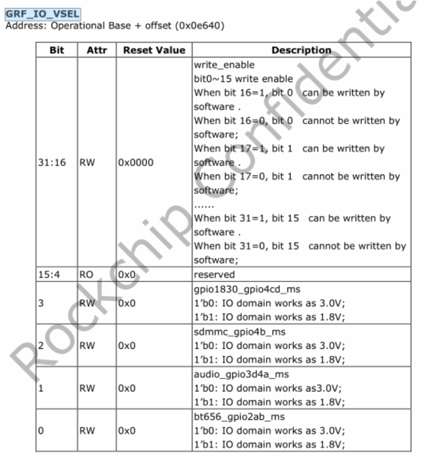
Technical figure from the Chinese source, PDF p.5.
GRF_IO_VSEL — Address: operational base + offset (0x0e640).
| Bit | Attr | Reset Value | Description |
|---|---|---|---|
| 31:16 | RW | 0x0000 | write_enable: bit0~15 write enable. When bit16=1, software can write bit0; when bit16=0, it cannot. When bit17=1, software can write bit1; when bit17=0, it cannot. …… When bit31=1, software can write bit15; when bit31=0, it cannot. |
| 15:4 | RO | 0x0 | Reserved |
| 3 | RW | 0x0 | gpio1830_gpio4cd_ms: 1’b0: IO domain works at 3.0V; 1’b1: IO domain works at 1.8V. |
| 2 | RW | 0x0 | sdmmc_gpio4b_ms: 1’b0: IO domain works at 3.0V; 1’b1: IO domain works at 1.8V. |
| 1 | RW | 0x0 | audio_gpio3d4a_ms: 1’b0: IO domain works at 3.0V; 1’b1: IO domain works at 1.8V. |
| 0 | RW | 0x0 | bt656_gpio2ab_ms: 1’b0: IO domain works at 3.0V; 1’b1: IO domain works at 1.8V. |
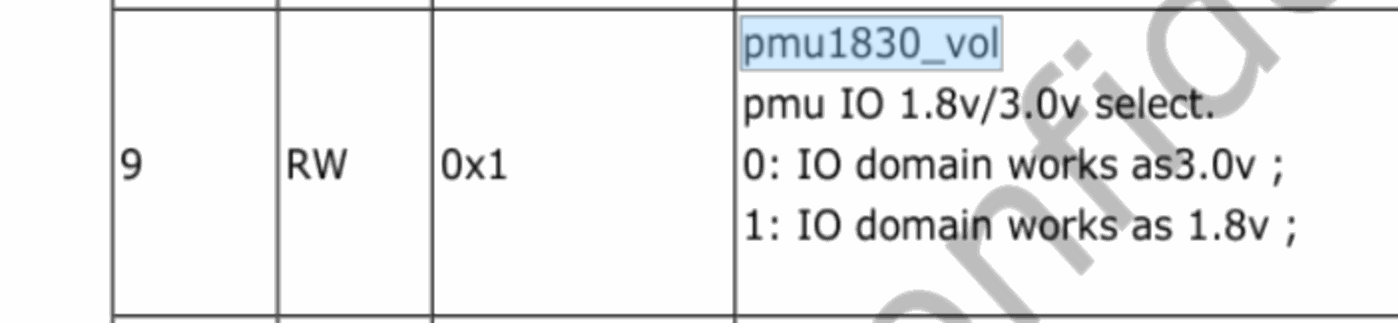
Technical figure from the Chinese source, PDF p.5.
| Bit | Attr | Reset Value | Description |
|---|---|---|---|
| 9 | RW | 0x1 | pmu1830_vol: PMU IO 1.8V/3.0V selection. 0: IO domain works at 3.0V; 1: IO domain works at 1.8V. |
After locating the registers by keyword, check the supply corresponding to the pins in the schematic. For example, suppose the entire row of gpio2 pins cannot be controlled correctly:
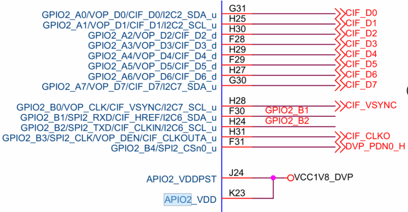
Technical figure from the Chinese source, PDF p.6.
This row of pins uses the APIO2 supply. In the SDK kernel directory, open kernel/Documentation/devicetree/bindings/power/rockchip-io-domain.txt. It describes the software definition of the APIO2 supply in detail:
Possible supplies for rk3399:
- bt656-supply: The supply connected to APIO2_VDD.
- audio-supply: The supply connected to APIO5_VDD.
- sdmmc-supply: The supply connected to SDMMC0_VDD.
- gpio1830 The supply connected to APIO4_VDD.
Possible supplies for rk3399 pmu-domains:
- pmu1830-supply:The supply connected to PMUIO2_VDD.
Search the dts directory for io_domain to find:
&io_domains {
    status = "okay";
    bt656-supply = <&vcc1v8_dvp >;
    audio-supply = <&vcca1v8_codec>;
    sdmmc-supply = <&vcc_sdio>;
    gpio1830-supply = <&vcc_3v0>;
};
Ensure that the corresponding software supply setting matches the hardware:
bt656-supply = <&vcc1v8_dvp>;
Inspect the debug-node information:
console:/ # cat sys/kernel/debug/regulator/regulator_summary
The 1.8V setting here is correct only if it agrees with the schematic. If it differs, change the setting to match.
1.2 U-Boot configuration
See section 9.13 of RKDocs/rk3399/Rockchip_RK3399_Developer_Guide_Android7.1_Software_CN&EN.pdf, which adds io-domain configuration in the rkdevelop branch of U-Boot. This functionality resolves the following issues:
It fixes incorrect IO levels or an inability to configure iomux caused by an incorrect io-domain setting in U-Boot. Without an io-domain setting in U-Boot, the chip uses its defaults until the kernel loads the correct DTS configuration, a period of approximately 3~4s. If an io-domain is connected to 3.0V but its default configuration is 1.8V, the voltage mismatch can damage the RK3399 IO.
Configure the kernel io-domain and confirm that U-Boot and the kernel contain these two commits (u-boot/drivers/power/rockchip-io-domain.c):
u-boot:
commit 5a4e354a116b45b8ac2311aaa3464a7e88cd13d5
Author: Jianqun Xu <jay.xu@rock-chips.com>
Date: Thu Mar 19 15:38:19 2020 +0800
power: support rockchip io-domain set
This patch should work with kernel dtb node property - "uboot-set" in io-domain node or pmu-io-domain node.
Change-Id: I86fa43d234091310ee08978ec42f5895fb010a8c
Signed-off-by: Jianqun Xu <jay.xu@rock-chips.com>
Signed-off-by: Wenping Zhang <wenping.zhang@rock-chips.com>
kernel:
commit f95ad65aabffa7450ff90a0dd4778cd5500de937
Author: Jianqun Xu <jay.xu@rock-chips.com>
Date: Fri Mar 20 09:52:57 2020 +0800
arm64: dts: rockchip: add 'uboot-set' in io-domain node for rk3399.
Add 'uboot-set' for io-domain node, which used by u-boot board init to set io domain.
Change-Id: Ia897e240c04d0b362551952278dadc8b4f2a8f2f
Signed-off-by: Jianqun Xu <jay.xu@rock-chips.com>
Signed-off-by: Wenping Zhang <wenping.zhang@rock-chips.com>
2. Developing GPIO in the kernel
This chapter introduces the configuration and methods for GPIO development in the kernel.
2.1 GPIO multiplexing
DTS configuration
The following configuration uses RK3588 Android12 as an example. To operate gpio3b7, configure enable-gpios = <&gpio3 RK_PB7 GPIO_ACTIVE_HIGH> in DTS. To prevent the pin being multiplexed to another function before the kernel starts and becoming unavailable as GPIO, use pinctrl-names and pinctrl-0 to select GPIO functionality. To request an IO interrupt, gpio3b6 illustrates configuration as a Schmitt-trigger input.
/{
    gpio_demo: gpio-demo {
        status = "okay";
        compatible = "rockchip,gpio-demo";
        enable-gpios = <&gpio3 RK_PB7 GPIO_ACTIVE_HIGH>;
        irq-gpios = <&gpio3 RK_PB6 GPIO_ACTIVE_HIGH>;
        pinctrl-names = "default";
        pinctrl-0 = <&gpio_pin &gpio_irq>;
    };
};
&pinctrl {
    gpio-pin {
        gpio_pin: gpio-pin {
            // Configure gpio3b7 iomux to GPIO
            rockchip,pins = <3 RK_PB7 RK_FUNC_GPIO &pcfg_pull_none>;
        };
    };
    gpio-irq {
        gpio_irq: gpio-irq {
            // Configure gpio3b6 iomux to GPIO and schmidt input mode
            rockchip,pins = <3 RK_PB6 RK_FUNC_GPIO &pcfg_pull_none_smt>;
        };
    };
};
Nodes referenced by pinctrl-0 must follow these rules:
They must be under the pinctrl node, use the function+group structure, and follow the other basic DTS rules. The function+group format is:
function {
    group {
        rockchip,pin = <gpiobank gpionum iomuxfunc &config>;
    };
};
iomuxfunc specifies the multiplexed function; RK_FUNC_GPIO selects GPIO. config sets pull-up, pull-down, Schmitt-trigger input mode and drive strength. See the SDK file rockchip-pinconf.dtsi; RK lists the available configurations under the DTS pinctrl node, as follows:
&pinctrl {
    pcfg_pull_up: pcfg-pull-up {
        bias-pull-up;
    };
    pcfg_pull_down: pcfg-pull-down {
        bias-pull-down;
    };
    pcfg_pull_none: pcfg-pull-none {
        bias-disable;
    };
    pcfg_pull_none_smt: pcfg-pull-none-smt {
        bias-disable;
        input-schmitt-enable;
    };
    pcfg_pull_none_drv_level_0: pcfg-pull-none-drv-level-0 {
        bias-disable;
        drive-strength = <0>;
    };
    ......
    pcfg_output_high: pcfg-output-high {
        output-high;
    };
    ......
    pcfg_output_low: pcfg-output-low {
        output-low;
    };
    ......
};
Here drive-strength = <2> selects drive-strength level 2, so 2 is written to the drive-strength register. For RK3588, the TRM lists the gpio2a0 drive-strength levels in the following figure; level 2 represents 50ohm.
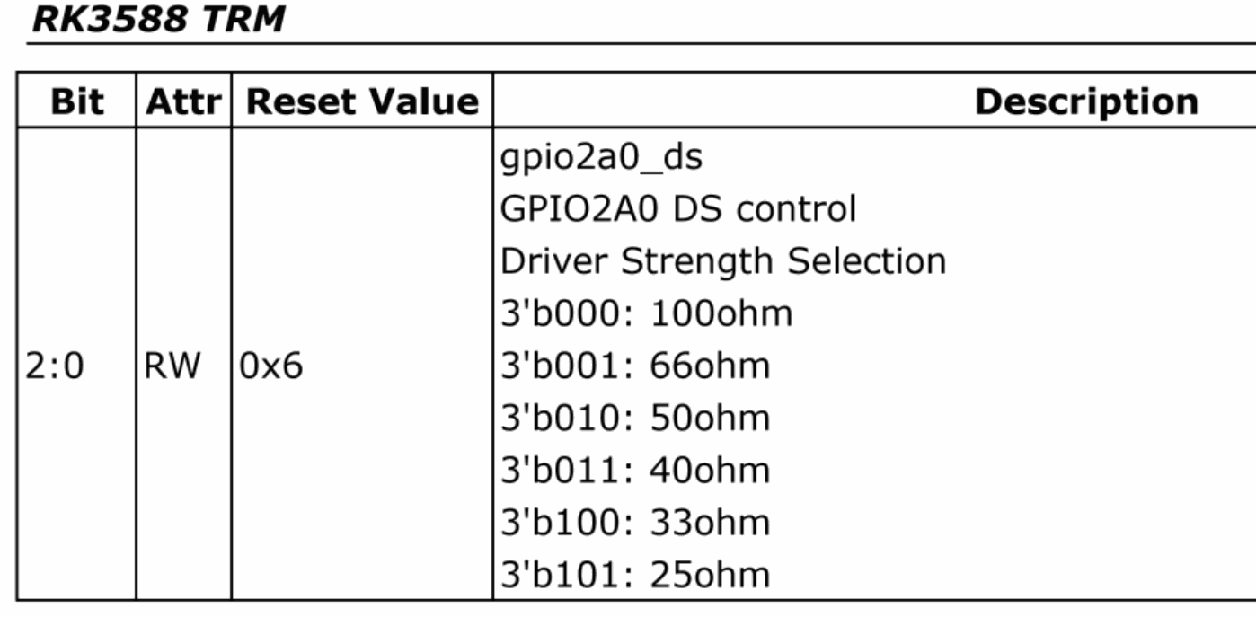
Technical figure from the Chinese source, PDF p.10.
RK3588 TRM
| Bit | Attr | Reset Value | Description |
|---|---|---|---|
| 2:0 | RW | 0x6 | gpio2a0_ds: GPIO2A0 DS control, driver-strength selection. 3’b000: 100ohm; 3’b001: 66ohm; 3’b010: 50ohm; 3’b011: 40ohm; 3’b100: 33ohm; 3’b101: 25ohm. |
User driver code
Using RK3588 Android12 as an example, once DTS is configured, the user driver reads that configuration to operate GPIO. It can request and operate GPIO using the following functions.
// Get the GPIO device. If multiple devices are used, the index parameter must be included
struct gpio_desc *gpiod_get(struct device *dev, const char *con_id,
                    enum gpiod_flags flags)
struct gpio_desc *gpiod_get_index(struct device *dev,
                      const char *con_id, unsigned int idx,
                      enum gpiod_flags flags)
// Release the GPIO device
void gpiod_put(struct gpio_desc *desc)
void gpiod_put_array(struct gpio_descs *descs)
// Set gpio input/output
int gpiod_direction_input(struct gpio_desc *desc)
int gpiod_direction_output(struct gpio_desc *desc, int value)
// Get/Set gpio value
int gpiod_get_value(const struct gpio_desc *desc);
void gpiod_set_value(struct gpio_desc *desc, int value);
//Get the GPIO IRQ interrupt number
int gpiod_to_irq(const struct gpio_desc *desc)
......
Example GPIO operation code for the user driver:
// SPDX-License-Identifier: GPL-2.0
/*
 * Copyright (c) 2020 Rockchip Electronics Co. Ltd.
 *
 * Author:Johnny Shi <nengqiang.shi@rock-chips.com>
 */
/* The following code is based on the RK3588 Android 12 platform */
#include <linux/gpio/consumer.h>
#include <linux/interrupt.h>
#include <linux/kernel.h>
#include <linux/math64.h>
#include <linux/module.h>
#include <linux/of_graph.h>
#include <linux/phy/phy.h>
#include <linux/platform_device.h>
static irqreturn_t irq_demo_handler(int irq, void *dev_id)
{
    printk("------irq_demo------\n");
    return IRQ_HANDLED;
}
static int gpio_demo_probe(struct platform_device *pdev)
{
    struct gpio_desc *enable_gpio, *irq_gpio;
    int irq;
    int ret;
    printk("------gpio_demo_probe------\n");
    // Get the gpio3b7 pin and set it as output
    enable_gpio = devm_gpiod_get_index(&pdev->dev, "enable", 0, GPIOD_OUT_HIGH);
    if (IS_ERR(enable_gpio)) {
        ret = PTR_ERR(enable_gpio);
         dev_err(&pdev->dev, "failed to request enable GPIO: %d\n", ret);
        return ret;
    }
    // Get the gpio3b6 pin and set it as input
    irq_gpio = devm_gpiod_get_index(&pdev->dev, "irq", 0, GPIOD_IN);
    if (IS_ERR(irq_gpio)) {
        ret = PTR_ERR(irq_gpio);
         dev_err(&pdev->dev, "failed to request irq GPIO: %d\n", ret);
        return ret;
    }
    // Get the gpio3b6 IRQ interrupt number and request IRQ
    irq = gpiod_to_irq(irq_gpio);
    ret = request_irq(irq, irq_demo_handler, IRQF_TRIGGER_FALLING, "demo_irq", NULL);
    if (ret) {
         dev_err(&pdev->dev, "failed to request IRQ: %d\n", ret);
        return ret;
    }
    // Set gpio3b7 pin output high
    gpiod_set_value(enable_gpio, 1);
    return 0;
}
static const struct of_device_id gpio_demo_of_match[] = {
    { .compatible = "rockchip,gpio-demo" },
    {}
};
static struct platform_driver gpio_demo_driver = {
    .driver = {
        .name = "gpio-demo",
        .of_match_table = of_match_ptr(gpio_demo_of_match),
    },
    .probe = gpio_demo_probe,
// .remove = gpio_demo_remove,
};
module_platform_driver(gpio_demo_driver);
MODULE_DESCRIPTION("Rockchip gpio demo driver");
MODULE_LICENSE("GPL v2");
According to DTS, the user driver obtains gpio3b7 using devm_gpiod_get_index(&pdev->dev, "enable", 0, GPIOD_OUT_HIGH). GPIO_ACTIVE_HIGH in DTS sets active-high polarity, and GPIOD_OUT_HIGH initializes gpio3b7 as an output. gpiod_set_value(enable_gpio, 1) drives gpio3b7 high. To request an IRQ as shown above, first obtain gpio3b6 with devm_gpiod_get_index(&pdev->dev, "irq", 0, GPIOD_IN) and initialize it as an input. Request the IRQ through gpiod_to_irq(irq_gpio) and request_irq(irq, irq_demo_handler, IRQF_TRIGGER_FALLING, "demo_irq", NULL).
2.2 GPIO input and output
In DTS, set pinctrl-names to default and configure the GPIO property in pinctrl-0 as pcfg_output_high or pcfg_output_low to directly output high or low. The driver automatically applies the GPIO properties in pinctrl-0 when it loads.
For example:
imx415: imx415@1a {
    compatible = "sony,imx415";
    reg = <0x1a>;
    clocks = <&cru CLK_MIPI_CAMARAOUT_M1>;
    clock-names = "xvclk";
    pinctrl-names = "default";
- pinctrl-0 = <&mipim0_camera1_clk>;
+ pinctrl-0 = <&mipim0_camera1_clk &test_gpio>; //添加一个test_gpio
    power-domains = <&power RK3588_PD_VI>;
    ......
}
&pinctrl {
    test {
        test_gpio: test-gpio {
            //GPIO3_B1配置为高电平输出,也可以配置为pcfg_output_low,低电平输出。
            rockchip,pins = <3 RK_PB1 RK_FUNC_GPIO &pcfg_output_high>;
        };
    };
}
For GPIO input, pcfg_pull_none or pcfg_pull_none_smt is generally sufficient.
2.3 Dynamically changing IO multiplexing
IO pin multiplexing can be changed dynamically: for example, a pin can serve as UART during one phase of kernel execution and as ordinary GPIO during another. The following configuration uses RK3588 Android12 as an example.
DTS configuration
Besides the four states defined by the kernel, pinctrl-names can specify custom states. The default state selects the uart3 pins and is automatically bound and applied by the kernel after the user driver matches; the driver need not apply it again. For custom states, see pinctrl-names=”iomux-exchange”. The driver can parse the state and dynamically select pin multiplexing as required.
/{
    iomux_exchange: iomux-exchange {
        compatible= "iomux-exchange-demo";
        pinctrl-names= "default", "iomux-exchange";
        pinctrl-0= <&uart3m0_xfer>;
        pinctrl-1= <&uart3m0_gpio>;
    };
    &pinctrl {
        uart3 {
            /omit-if-no-ref/
            uart3m0_xfer: uart3m0-xfer {
                rockchip,pins =
                    /* uart3_rx_m0 */
                    <1 RK_PC0 10 &pcfg_pull_up>,
                    /* uart3_tx_m0 */
                    <1 RK_PC1 10 &pcfg_pull_up>;
            };
        uart3-gpio{
            uart3m0_gpio: uart3m0-gpio {
                rockchip,pins =
                    <1 RK_PC0 RK_FUNC_GPIO &pcfg_pull_none>,
                    <1 RK_PC1 RK_FUNC_GPIO &pcfg_pull_none>;
            };
        };
    };
};
User driver code
The driver obtains pinctrl resources with devm_pinctrl_get, obtains the custom GPIO state with pinctrl_lookup_state, and applies the IO state with pinctrl_select_state. Example driver code:
// SPDX-License-Identifier: GPL-2.0
/*
 * Copyright (c) 2020 Rockchip Electronics Co. Ltd.
 *
 * Author:Johnny Shi <nengqiang.shi@rock-chips.com>
 */
/* The following code is based on the RK3588 Android 12 platform */
#include <linux/gpio/consumer.h>
#include <linux/interrupt.h>
#include <linux/kernel.h>
#include <linux/math64.h>
#include <linux/module.h>
#include <linux/of_graph.h>
#include <linux/phy/phy.h>
#include <linux/platform_device.h>
#include <linux/pinctrl/consumer.h>
struct pinctrl *uart_pinctrl;
struct pinctrl_state *uart_default;//uart
struct pinctrl_state *uart_gpio;//gpio
static int iomux_exchange(int select) {
    int ret = 0;
    if (select) {
        ret = pinctrl_select_state(uart_pinctrl, uart_gpio);
    } else {
        ret = pinctrl_select_state(uart_pinctrl, uart_default);
    }
    return ret;
}
static int iomux_exchange_demo_probe(struct platform_device *pdev)
{
    printk("------iomux_exchange_demo_probe------\n");
    uart_pinctrl = devm_pinctrl_get(&pdev->dev);
    if (IS_ERR_OR_NULL(uart_pinctrl)) {
        printk("Failed to get pin ctrl\n");
        return PTR_ERR(uart_pinctrl);
    }
    // Gets the pinctrl status property of "default"
    uart_default = pinctrl_lookup_state(uart_pinctrl, "default");
    if (IS_ERR_OR_NULL(uart_default)) {
        printk("Failed to lookup pinctrl default state\n");
        return PTR_ERR(uart_default);
    }
    // Get the custom "iomux-exchange" pinctrl status properties
    uart_gpio = pinctrl_lookup_state(uart_pinctrl, "iomux-exchange");
    if (IS_ERR_OR_NULL(uart_gpio)) {
        printk("Failed to lookup pinctrl iomux-exchange state\n");
        return PTR_ERR(uart_gpio);
    }
    iomux_exchange(1);
    //iomux_exchange(0);
    return 0;
}
static const struct of_device_id iomux_exchange_demo_of_match[] = {
    { .compatible = "iomux-exchange-demo" },
    {}
};
static struct platform_driver iomux_exchange_demo_driver = {
    .driver = {
        .name = "iomux-exchange-demo",
        .of_match_table = of_match_ptr(iomux_exchange_demo_of_match),
    },
    .probe = iomux_exchange_demo_probe,
// .remove = iomux_exchange_demo_remove,
};
module_platform_driver(iomux_exchange_demo_driver);
MODULE_DESCRIPTION("Rockchip iomux exchange demo driver");
MODULE_LICENSE("GPL v2");
If the code above does not call iomux_exchange(1), the pins default to UART. After boot, enter the following command to inspect IO multiplexing:
console:/ # cat sys/kernel/debug/pinctrl/pinctrl-rockchip-pinctrl/pinmux-pins
......
pin 44 (gpio1-12): (MUX UNCLAIMED) (GPIO UNCLAIMED)
pin 45 (gpio1-13): fde60000.dp gpio1:45 function dp group dp1-hpd
pin 46 (gpio1-14): 5-001a (GPIO UNCLAIMED) function mipi group mipim0-camera1-clk
pin 47 (gpio1-15): (MUX UNCLAIMED) (GPIO UNCLAIMED)
pin 48 (gpio1-16): iomux-exchange (GPIO UNCLAIMED) function uart3 group uart3m0-xfer
pin 49 (gpio1-17): iomux-exchange (GPIO UNCLAIMED) function uart3 group uart3m0-xfer
pin 50 (gpio1-18): 7-0011 (GPIO UNCLAIMED) function i2s0 group i2s0-mclk
pin 51 (gpio1-19): fe470000.i2s (GPIO UNCLAIMED) function i2s0 group i2s0-idle
pin 52 (gpio1-20): (MUX UNCLAIMED) gpio1:52
pin 53 (gpio1-21): fe470000.i2s (GPIO UNCLAIMED) function i2s0 group i2s0-idle
......
gpio1-16 and gpio1-17 are configured as UART pins. After calling iomux_exchange(1), inspect them again:
console:/ # cat sys/kernel/debug/pinctrl/pinctrl-rockchip-pinctrl/pinmux-pins
......
pin 44 (gpio1-12): (MUX UNCLAIMED) (GPIO UNCLAIMED)
pin 45 (gpio1-13): fde60000.dp gpio1:45 function dp group dp1-hpd
pin 46 (gpio1-14): 5-001a (GPIO UNCLAIMED) function mipi group mipim0-camera1-clk
pin 47 (gpio1-15): (MUX UNCLAIMED) (GPIO UNCLAIMED)
pin 48 (gpio1-16): iomux-exchange (GPIO UNCLAIMED) function uart3-gpio group uart3m0-gpio
pin 49 (gpio1-17): iomux-exchange (GPIO UNCLAIMED) function uart3-gpio group uart3m0-gpio
pin 50 (gpio1-18): 7-0011 (GPIO UNCLAIMED) function i2s0 group i2s0-mclk
pin 51 (gpio1-19): fe470000.i2s (GPIO UNCLAIMED) function i2s0 group i2s0-idle
pin 52 (gpio1-20): (MUX UNCLAIMED) gpio1:52
pin 53 (gpio1-21): fe470000.i2s (GPIO UNCLAIMED) function i2s0 group i2s0-idle
......
gpio1-16 and gpio1-17 have successfully switched to GPIO functionality.
3. Developing GPIO in U-Boot
GPIO can be operated in U-Boot by directly reading and writing register addresses with readl and writel, but that code is not portable. This section instead describes operation through a U-Boot driver. Using RK3588 Android12 as the example, the U-Boot DTS configuration and driver code are shown below.
3.1 Developing a U-Boot LED driver
DTS configuration
U-Boot has its own DTS files. The corresponding DTB is generated automatically during compilation and appended to u-boot.bin. GPIO DTS configuration in U-Boot is the same as in the kernel, except that the node must include u-boot,dm-spl or u-boot,dm-pre-reloc.
/{
    leds {
        compatible = "gpio-leds";
        status = "okay";
        u-boot,dm-spl;
        blue-led {
            u-boot,dm-spl;
            gpios = <&gpio2 RK_PA1 GPIO_ACTIVE_LOW>;
            label = "blue_full";
            default-state = "on";
        };
        green-led {
            u-boot,dm-spl;
            gpios = <&gpio2 RK_PA0 GPIO_ACTIVE_LOW>;
            label = "green_led";
            default-state = "on";
        };
    };
};
Note: gpio-leds configuration in DTS is normally placed in the kernel. The label option must be supplied; otherwise led_gpio.c fails during bind. The following patch prints the label setting:
diff --git a/drivers/led/led_gpio.c b/drivers/led/led_gpio.c
index 56702a1417..18062f2ac1 100644
--- a/drivers/led/led_gpio.c
+++ b/drivers/led/led_gpio.c
@@ -112,6 +112,7 @@ static int led_gpio_bind(struct udevice *parent)
                const char *label;
                label = ofnode_read_string(node, "label");
+ printf("%s: label %s\n", __func__, label);
                if (!label) {
                        debug("%s: node %s has no label\n", __func__,
                              ofnode_get_name(node));
After building U-Boot, inspect the DTB contents with fdtdump:
fdtdump ./u-boot.dtb | less
User driver code
The following introduces the LED driver in U-Boot. First enable these options:
/u-boot/configs/rk3588_defconfig
CONFIG_LED=y
CONFIG_LED_GPIO=y
The framework code is shown below:
u-boot/drivers/led/led-uclass.c // 默认编译
u-boot/drivers/led/led_gpio.c // 支持 compatible = "gpio-leds"
Relevant code interfaces
// 获取led device
int led_get_by_label(const char *label, struct udevice **devp);
// 设置/获取led状态
int led_set_state(struct udevice *dev, enum led_state_t state);
enum led_state_t led_get_state(struct udevice *dev);
// 忽略,目前未做底层驱动实现
int led_set_period(struct udevice *dev, int period_ms);
Calling led_get_by_label is sufficient to turn on the LED. In the example below, call led_get_by_label from board_late_init. After the system starts, the LEDs connected to gpio2a0 and gpio2a1 should light.
/u-boot/arch/arm/mach-rockchip/board.c
#include <led.h>
int board_late_init(void)
{
    struct udevice *led_dev;
    ...
    led_get_by_label("blue_full", &led_dev);
    led_set_state(led_dev, LEDST_ON);
    ...
}
Unlike the kernel, U-Boot does not automatically initiate probe for registered device-driver pairs during initialization, even though it uses a device-driver model. The user must explicitly trigger probe. Thus led_gpio_probe runs only after the user calls led_get_by_label. The core operation of led_get_by_label is device_probe, which invokes the LED driver’s probe. led_set_state can then control whether the LED is on or off.
Using the LED driver as a reference, a custom GPIO driver for U-Boot can be designed. The interface for obtaining a user device driver is:
int uclass_get_device(enum uclass_id id, int index, struct udevice **devp);
int uclass_get_device_by_name(enum uclass_id id, const char *name,
struct udevice **devp);
int uclass_get_device_by_seq(enum uclass_id id, int seq, struct udevice **devp);
int uclass_get_device_by_of_offset(enum uclass_id id, int node, struct udevice
**devp);
int uclass_get_device_by_ofnode(enum uclass_id id, ofnode node, struct udevice
**devp);
int uclass_get_device_by_phandle_id(enum uclass_id id,
int phandle_id, struct udevice **devp);
int uclass_get_device_by_phandle(enum uclass_id id,
struct udevice *parent, struct udevice **devp);
int uclass_get_device_by_driver(enum uclass_id id,
const struct driver *drv, struct udevice
**devp);
int uclass_get_device_tail(struct udevice *dev, int ret, struct udevice **devp);
......
The GPIO operation interfaces are:
// 申请/释放GPIO
int gpio_request_by_name(struct udevice *dev, const char *list_name,
int index, struct gpio_desc *desc, int flags);
int gpio_request_by_name_nodev(ofnode node, const char *list_name, int index,
struct gpio_desc *desc, int flags);
int gpio_request_list_by_name(struct udevice *dev, const char *list_name,
struct gpio_desc *desc_list, int max_count, int
flags);
int gpio_request_list_by_name_nodev(ofnode node, const char *list_name,
struct gpio_desc *desc_list, int max_count,
int flags);
int dm_gpio_free(struct udevice *dev, struct gpio_desc *desc)
// 配置GPIO方向。@flags:GPIOD_IS_OUT(输出)和 GPIOD_IS_IN(输入)
int dm_gpio_set_dir_flags(struct gpio_desc *desc, ulong flags);
// 设置/获取GPIO电平
int dm_gpio_get_value(const struct gpio_desc *desc)
int dm_gpio_set_value(const struct gpio_desc *desc, int value)
udevice is obtained through uclass_id. The LED driver registration is shown below:
U_BOOT_DRIVER(led_gpio) = {
  .name = "gpio_led",
  .id = UCLASS_LED,
  .of_match = led_gpio_ids,
  .ops = &gpio_led_ops,
  .priv_auto_alloc_size = sizeof(struct led_gpio_priv),
  .bind = led_gpio_bind,
  .probe = led_gpio_probe,
  .remove = led_gpio_remove,
};
UCLASS_LED is defined in u-boot/include/dm/uclass-id.h.
3.2 Developing a U-Boot GPIO driver
The LED driver above already exists in U-Boot; users only need to configure DTS and call its interfaces. The following is a GPIO driver development demo for U-Boot. Enable these options:
/u-boot/configs/rk3588_defconfig
CONFIG_DM_GPIO=y
CONFIG_GPIO_HOG=y
CONFIG_ARCH_ROCKCHIP=y
CONFIG_SPL_GPIO_SUPPORT=y
DTS configuration
For example, to operate gpio3b7, configure U-Boot DTS as follows:
gpio_uboot_demo {
    u-boot,dm-pre-reloc;
    compatible="gpio_uboot_demo";
    enable-gpios = <&gpio3 RK_PB7 GPIO_ACTIVE_HIGH>;
    status = "okay";
};
&gpio3 {
    u-boot,dm-pre-reloc;
    status = "okay";
};
User driver code
/*
 * Copyright (c) 2015 Google, Inc
 * Written by Simon Glass <sjg@chromium.org>
 *
 * SPDX-License-Identifier: GPL-2.0+
 */
/* The following code is based on the RK3588 Android 12 platform */
#include <common.h>
#include <dm.h>
#include <errno.h>
#include <asm/gpio.h>
#include <dm/lists.h>
#include <dm/ofnode.h>
static int gpio_uboot_demo_probe(struct udevice *dev)
{
    struct gpio_desc gpio_uboot ;
    int ret;
    printf("----gpio_uboot_demo_probe----\n");
    ret = gpio_request_by_name(dev, "enable-gpios", 0, &gpio_uboot, GPIOD_IS_OUT);
    if(ret)
    {
        printf("can not get eepro_wp gpio\n");
    }
    dm_gpio_set_value(&gpio_uboot, 1);
    return 0;
}
static int gpio_uboot_demo_remove(struct udevice *dev)
{
    printf("----gpio_uboot_demo_remove----\n");
    return 0;
}
static const struct udevice_id gpio_uboot_demo_ids[] = {
    { .compatible = "gpio_uboot_demo" },
    { }
};
U_BOOT_DRIVER(gpio_uboot_demo) = {
    .name = "gpio_uboot_demo",
    .id = UCLASS_GPIO,
    .of_match = gpio_uboot_demo_ids,
    .probe = gpio_uboot_demo_probe,
    .remove = gpio_uboot_demo_remove,
};
The driver obtains gpio3b7 with gpio_request_by_name(dev, "enable-gpios", 0, &gpio_uboot, GPIOD_IS_OUT) and configures it as an output. The user must explicitly call the relevant interface to execute the GPIO probe function, as follows:
/u-boot/arch/arm/mach-rockchip/board.c
int board_late_init(void)
{
    struct udevice *dev;
    ...
    uclass_get_device_by_driver(UCLASS_GPIO, DM_GET_DRIVER(gpio_uboot_demo), &dev);
    ...
}
Calling uclass_get_device_by_driver from board_late_init ultimately invokes the driver’s probe above. dm_gpio_set_value(&gpio_uboot, 1) drives the output high.
4. GPIO development in user space
There are many ways to work with GPIO in user space; this section uses the common echo command as an example. The Linux kernel provides a user-space GPIO debugging interface under /sys/class/gpio/:
console:/sys/class/gpio# ls
export gpiochip128 gpiochip509 gpiochip96
gpiochip0 gpiochip32 gpiochip64 unexport
The export file tells the system to export the GPIO pin number to be controlled; unexport removes that export. gpiochipN stores information about the system’s GPIO registers, including the base pin number controlled by each register, its name and the total number of pins.
As an example, export gpio1b1. First calculate its number: pin number = base of the controlling register + bit number within that register. gpio1b1 = 32 + 9 = 41. Export gpio1b1:
console:/sys/class/gpio# echo 41 > export
Set the direction: in means input and out means output:
console:/sys/class/gpio/gpio41# echo out > direction
Read the direction:
console:/sys/class/gpio/gpio41# cat direction
Set the output:
console:/sys/class/gpio/gpio41# echo 1 > value
Read the input/output value:
console:/sys/class/gpio/gpio41# cat value
Unexport the pin:
console:/sys/class/gpio# echo 41 > unexport
These operations require the IO to be multiplexed as GPIO. If another function is selected, its GPIO input/output cannot be operated. Check multiplexing first. Besides reading registers with the io tool, the following command shows multiplexing and configuration for all pins:
console:/ # cat sys/kernel/debug/pinctrl/pinctrl-rockchip-pinctrl/pinmux-pins
Pinmux settings per pin
Format: pin (name): mux_owner gpio_owner hog?
pin 0 (gpio0-0): (MUX UNCLAIMED) (GPIO UNCLAIMED)
pin 1 (gpio0-1): (MUX UNCLAIMED) (GPIO UNCLAIMED)
pin 2 (gpio0-2): (MUX UNCLAIMED) (GPIO UNCLAIMED)
pin 3 (gpio0-3): (MUX UNCLAIMED) (GPIO UNCLAIMED)
pin 4 (gpio0-4): (MUX UNCLAIMED) gpio0:4
pin 5 (gpio0-5): (MUX UNCLAIMED) gpio0:5
pin 6 (gpio0-6): ff420030.pwm (GPIO UNCLAIMED) function pwm3a group pwm3a-pin
pin 7 (gpio0-7): fe320000.dwmmc (GPIO UNCLAIMED) function sdmmc group sdmcc-cd
pin 8 (gpio0-8): (MUX UNCLAIMED) (GPIO UNCLAIMED)
pin 9 (gpio0-9): (MUX UNCLAIMED) gpio0:9
pin 10 (gpio0-10): (MUX UNCLAIMED) gpio0:10
......
console:/ # cat sys/kernel/debug/gpio
gpiochip0: GPIOs 0-31, parent: platform/pinctrl, gpio0:
 gpio-1 ( |vcc3v0_sd ) out hi
 gpio-4 ( |bt_default_wake_host) in lo
 gpio-5 ( |GPIO Key Power ) in hi
 gpio-9 ( |bt_default_reset ) out lo
 gpio-10 ( |reset ) out hi
 gpio-11 ( |spk-con ) out lo
gpiochip1: GPIOs 32-63, parent: platform/pinctrl, gpio1:
 gpio-34 ( |int-n ) in hi
 gpio-45 ( |enable ) out hi
gpiochip2: GPIOs 64-95, parent: platform/pinctrl, gpio2:
 gpio-64 ( |vbus-5v ) out lo
 gpio-83 ( |bt_default_rts ) in hi
 gpio-90 ( |bt_default_wake ) in lo
gpiochip3: GPIOs 96-127, parent: platform/pinctrl, gpio3:
 gpio-111 ( |mdio-reset ) out hi
gpiochip4: GPIOs 128-159, parent: platform/pinctrl, gpio4:
 gpio-150 ( |? ) out hi
 gpio-153 ( |vcc5v0_host ) out hi
 gpio-157 ( |enable ) out hi
 gpio-158 ( |vcc_lcd ) out hi
5. IO suspend and wakeup configuration
Chip-level suspend/wakeup operations are now mainly implemented in ATF, whose relevant code is not open. Different low-power modes entered during system sleep can be selected through DTS to meet product requirements. Projects require different wakeup sources; enable the appropriate sources in DTS.
The standby sequence generally shuts down power domains, module IPs, clocks and PLLs; puts DDR into self-refresh; switches the system bus to a low-speed clock (24M or 32K); powers off vdd_arm/vdd_log; and configures wakeup sources. To accommodate different standby requirements, the settings are passed to trust during boot through DTS nodes. RK3588 example:
arch/arm64/boot/dts/rockchip/rk3588s.dtsi
rockchip_suspend: rockchip-suspend {
        compatible = "rockchip,pm-rk3588";
        status = "disabled";
        // Set the sleep log switch. 0: printing is disabled, 1: printing is enabled
        rockchip,sleep-debug-en = <0>;
         // Sleep configuration
        rockchip,sleep-mode-config = <
                (0
                | RKPM_SLP_ARMOFF_LOGOFF //进入深度休眠断电vdd_arm和vdd_log
                | RKPM_SLP_PMU_PMUALIVE_32K //进入深度休眠时使用32K时钟源作为系统时钟
                | RKPM_SLP_PMU_DIS_OSC //关闭24M晶振,最低功耗模式时可使能
                | RKPM_SLP_32K_EXT //休眠时的32K时钟源是否选用外部的32K钟源
                )
        >;
        // Wakeup source configuration
        rockchip,wakeup-config = <
                (0
                | RKPM_GPIO_WKUP_EN //GPIO0唤醒
                )
        >;
};
5.1 Configuring GPIO wakeup
On RK3588, the GPIO0 pin supply is enabled during suspend by default and needs no additional configuration. To use a GPIO outside GPIO0 as a wakeup source, configure the following:
Keep this GPIO supply enabled during suspend.
vdd_log_s0: DCDC_REG3 {
    regulator-always-on;
    regulator-boot-on;
    regulator-min-microvolt = <675000>;
    regulator-max-microvolt = <750000>;
    regulator-ramp-delay = <12500>;
    regulator-name = "vdd_log_s0";
    regulator-state-mem {
    // regulator-off-in-suspend;
    regulator-on-in-suspend;
    regulator-suspend-microvolt = <750000>;
    };
};
regulator-off-in-suspend turns this supply off during suspend. To keep it on, change it to regulator-on-in-suspend.
Configure the rockchip_suspend node.
&rockchip_suspend {
        status = "okay";
        rockchip,sleep-debug-en = <1>;
        rockchip,sleep-mode-config = <
                (0
                 // | RKPM_SLP_ARMOFF_LOGOFF
                | RKPM_SLP_ARMOFF_DDRPD
                | RKPM_SLP_PMU_PMUALIVE_32K
                | RKPM_SLP_PMU_DIS_OSC
                | RKPM_SLP_32K_EXT
                )
        >;
        rockchip,wakeup-config = <
                (0
                | RKPM_GPIO_WKUP_EN
                | RKPM_CPU0_WKUP_EN
                )
        >;
};
In rockchip_suspend, RKPM_SLP_ARMOFF_LOGOFF powers off vdd_arm and vdd_log. Change it to RKPM_SLP_ARMOFF_DDRPD to retain vdd_log. Also configure RKPM_CPU0_WKUP_EN in rockchip_suspend.
Not every GPIO can be a wakeup source. Check PMU_WAKEUP_INT_CON in the TRM; many platforms support wakeup only from the GPIO0 group.
5.2 Configuring GPIO levels during suspend
RK3399 example:
&rockchip_suspend {
    status = "okay";
+ rockchip,power-ctrl =
+ <&gpio1 17 GPIO_ACTIVE_HIGH>, //配置休眠时GPIO1_C1为高电平
+ <&gpio1 14 GPIO_ACTIVE_HIGH>; //配置休眠时GPIO1_B6为高电平
rockchip,power-ctrl can select only GPIOs on PMUIO1/2. Prefer GPIO0; otherwise the IO state cannot be retained after suspend. The new suspend framework restores IOs in non-PMU-controlled power domains to their default state during suspend.
6. GPIO expanders
This chapter describes basic configuration and use of GPIO expanders. PCA9555 is the example: a 16-bit general-purpose GPIO expander with interrupt support and weak pull-up resistors for I2c bus/SMBus applications.
DTS configuration
&i2c6 {
    status = "okay";
    pca9555_20: pca9555_20@20 {
        compatible = "nxp,pca9555";
        reg = <0x20>;
    };
    imx586: imx586@1a {
        compatible = "sony,imx586";
        status = "okay";
        reset-gpio-index = <503>;
        ......
    };
};
reset-gpio-index is the GPIO number, which can be confirmed using cat /sys/kernel/debug/gpio.
Driver calls
ret |= of_property_read_u32(node, "reset-gpio-index",
        &test->reset_gpio_index);
gpio_to_desc(test->reset_gpio_index);
7. Emulating I2C with GPIO
This chapter describes basic GPIO-based I2C configuration. The corresponding driver is kernel/drivers/i2c/busses/i2c-gpio.c.
Config options
Set CONFIG_I2C_GPIO=y in defconfig or select GPIO-based bitbanging I2C in menuconfig.
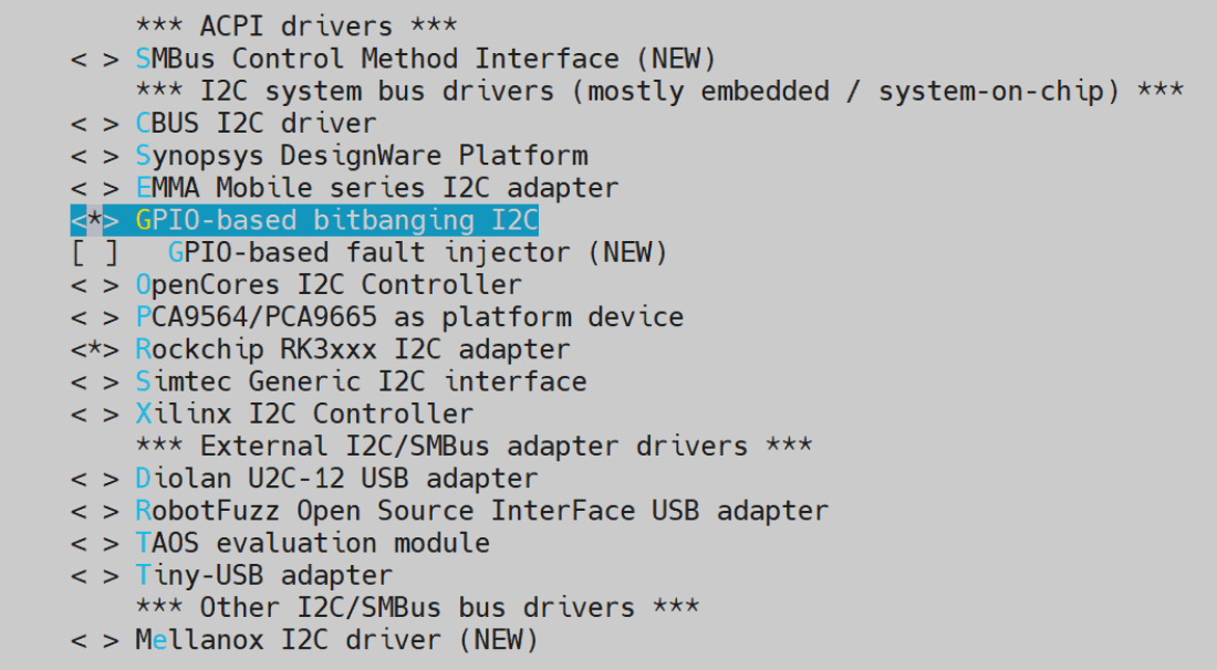
Technical figure from the Chinese source, PDF p.26.
The corresponding option is:
Device Drivers->
    I2C support --->
        I2C Hardware Bus support --->
            <*> GPIO-based bitbanging I2C
DTS configuration
i2c9: i2c@9 {
    compatible = "i2c-gpio";
    pinctrl-names = "default";
    pinctrl-0 = <&i2c9_xfer>;
    scl-gpios = <&gpio3 RK_PB3 GPIO_ACTIVE_HIGH>; //scl
    sda-gpios = <&gpio3 RK_PB4 GPIO_ACTIVE_HIGH>; //sda
    i2c-gpio,delay-us = <2>; /* ~100 kHz */
    #address-cells = <1>;
    #size-cells = <0>;
};
&pinctrl {
    i2c9 {
        /omit-if-no-ref/
        i2c9_xfer: i2c9-xfer {
            rockchip,pins =
                /* i2c9_scl */
                <3 RK_PB3 0 &pcfg_pull_none_smt>,
                /* i2c9_sda */
                <3 RK_PB4 0 &pcfg_pull_none_smt>;
        };
    };
};
8. GPIO debugging tools
This chapter introduces GPIO debugging tools.
8.1 IO tool
Rockchip platforms provide the IO tool to directly read and set register values for debugging.
8.1.1 IO tool in the kernel stage
Android10 and later require manual debugging configuration because of security standards. For example, on RK3399 Android12, enable these options to use IO commands:
kernel-5.10/kernel/configs/android-11.config
CONFIG_DEVMEM=y
Enter io and press Enter in the serial terminal or adb to list detailed command parameters.
console:/# io
Raw memory i/o utility - $Revision: 1.5 $
io -v -1|2|4 -r|w [-l <len>] [-f <file>] <addr> [<value>]
    -v Verbose, asks for confirmation
    -1|2|4 Sets memory access size in bytes (default byte)
    -l <len> Length in bytes of area to access (defaults to
               one access, or whole file length)
    -r|w Read from or Write to memory (default read)
    -f <file> File to write on memory read, or
               to read on memory write
    <addr> The memory address to access
    <val> The value to write (implies -w)
Examples:
    io 0x1000 Reads one byte from 0x1000
    io 0x1000 0x12 Writes 0x12 to location 0x1000
    io -2 -l 8 0x1000 Reads 8 words from 0x1000
    io -r -f dmp -l 100 200 Reads 100 bytes from addr 200 to file
    io -w -f img 0x10000 Writes the whole of file to memory
Note access size (-1|2|4) does not apply to file based accesses.
Querying GPIO multiplexing with the IO tool
Using RK3399 as an example, consult its TRM register descriptions to determine IO multiplexing. For gpio4b0, the schematic shows these possible functions:
GPIO4_B0/SDMMC0_D0/UART2A_RX_u
Search for gpio4b0 in the RK3399 TRM to find this register description:
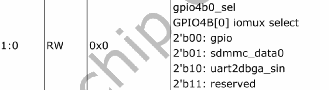
Technical figure from the Chinese source, PDF p.28.
| Bit | Attr | Reset Value | Description |
|---|---|---|---|
| 1:0 | RW | 0x0 | gpio4b0_sel: GPIO4B[0] iomux selection. 2’b00: gpio; 2’b01: sdmmc_data0; 2’b10: uart2dbga_sin; 2’b11: reserved. |
The TRM identifies GRF as the register base and 0x0e024 as its offset:

Technical figure from the Chinese source, PDF p.28.
GRF_GPIO4B_IOMUX — Address: operational base + offset (0x0e024). GPIO4B iomux control.
Search for address mapping in the datasheet and locate the GRF base address:
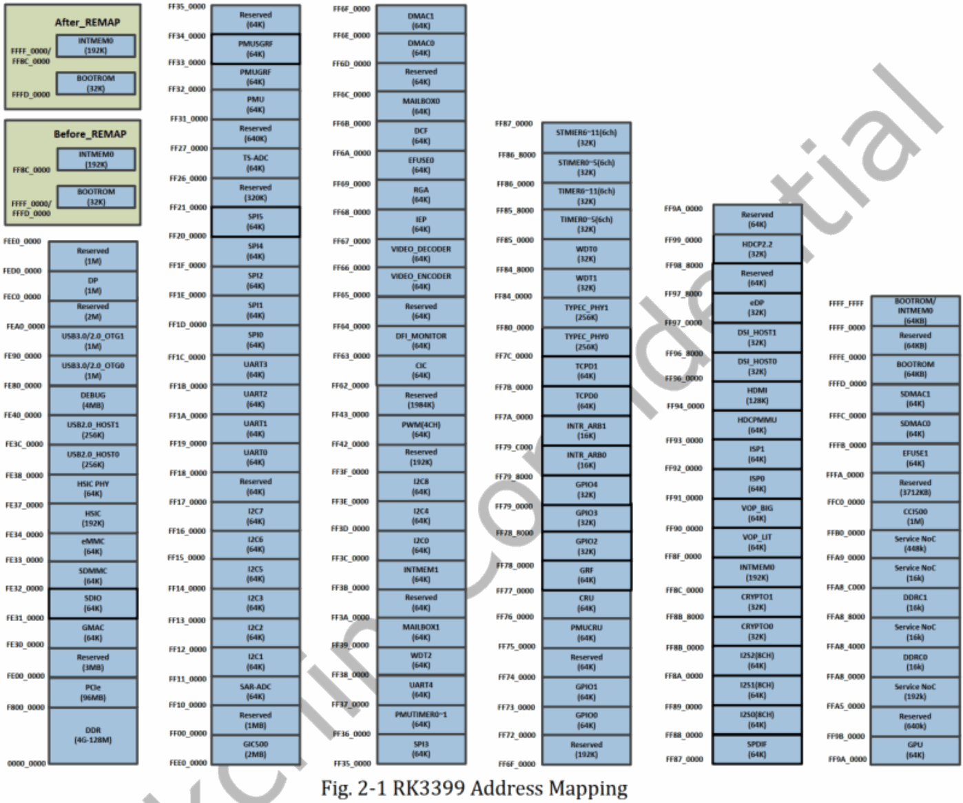
Technical figure from the Chinese source, PDF p.29.
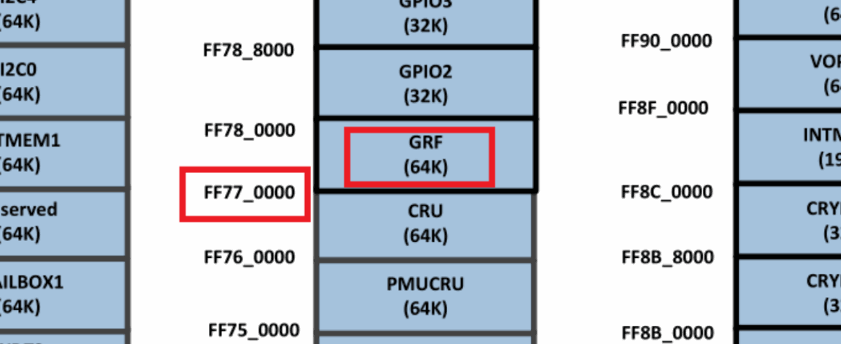
Technical figure from the Chinese source, PDF p.29.
Add the offset to the GRF base to obtain the gpio4b0 multiplexing register address, 0xff77e024. Enter in the serial terminal or adb:
console:/ # io -4 -l 0x100 0xff77e024
ff77e024: 00000555 0000855f 00000000 00000000
ff77e034: 00000000 00000000 00000000 000002a5
ff77e044: 00005450 0000ff03 00000143 00000000
ff77e054: 00004010 00000001 00000000 0000aa80
ff77e064: 00000455 00002040 0000aaa1 00000000
ff77e074: 00000000 00000000 00000000 00000000
ff77e084: 00000000 00000000 00000000 00000000
ff77e094: 00000000 00000000 00000000 00000000
ff77e0a4: 000000ff 00000000 00000000 00000000
ff77e0b4: 00000000 00000000 00000000 00000000
ff77e0c4: 00000000 00000000 00000000 00000000
ff77e0d4: 00000000 00000000 00000000 00000000
ff77e0e4: 00000000 00000000 00000000 00000000
ff77e0f4: 00000000 00000000 00000000 00000000
ff77e104: 00000000 00000000 00000000 0000b01b
ff77e114: 00000001 00003000 00000000 00000018
The first output line is:
ff77e024: 00000555 0000855f 00000000 00000000
The four values correspond to these addresses:
0xff77e024、0xff77e028、0xff77e02c、0xff77e030
Correspondence in hexadecimal:
0xff77e024:00000555
Convert 0x555 to binary and pad to 32 bits:
0000 0000 0000 0000 0000 0101 0101 0101
The converted value runs from least significant on the right to most significant on the left: the rightmost bit is bit 0 and the leftmost is bit 31. Match these bits against GRF_GPIO4B_IOMUX to interpret the result.
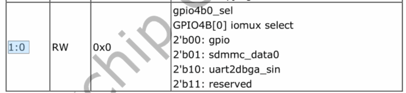
Technical figure from the Chinese source, PDF p.30.
| Bit | Attr | Reset Value | Description |
|---|---|---|---|
| 1:0 | RW | 0x0 | gpio4b0_sel: GPIO4B[0] iomux selection. 2’b00: gpio; 2’b01: sdmmc_data0; 2’b10: uart2dbga_sin; 2’b11: reserved. |
In the binary conversion of the serial output, bits [1:0] are 01, selecting sdmmc_data0. This confirms the current gpio4b0 multiplexing. If that is not the desired state, locate the code that selected it.
How can multiplexing be located in the code? Suppose gpio4b0 should be GPIO driven high/low, but the query reports sdmmc_data0. First find the sdmmc node in DTS and check whether its pinctrl property also references this GPIO.
Writing registers with the IO tool
To temporarily write a register for an experiment, use io -w.
For example, after reading the register with io -4 -r 0xff77e024, write 1 to bit 0 of 0xff77e024 as follows:
Why must bit 16 in the hexadecimal value following the register address be 1? Bits 16 through 31 are write-enable bits and default to 0, meaning writing is disabled. To write bit 0, its corresponding write-enable bit 16 must also be set to 1. This follows the register description:
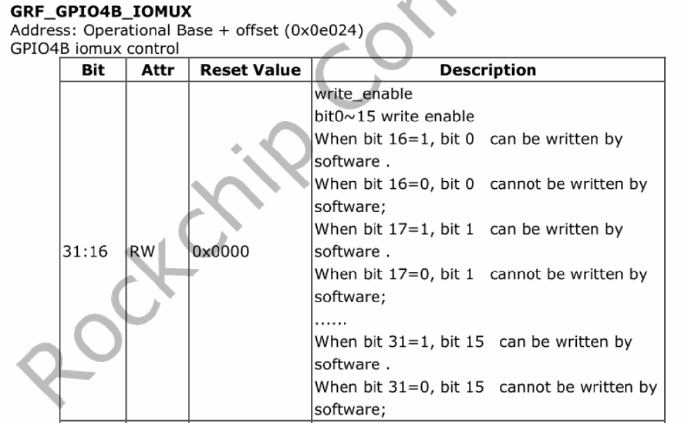
Technical figure from the Chinese source, PDF p.31.
GRF_GPIO4B_IOMUX — Address: operational base + offset (0x0e024). GPIO4B iomux control.
| Bit | Attr | Reset Value | Description |
|---|---|---|---|
| 31:16 | RW | 0x0000 | write_enable: bit0~15 write enable. When bit16=1, software can write bit0; when bit16=0, it cannot. When bit17=1, software can write bit1; when bit17=0, it cannot. …… When bit31=1, software can write bit15; when bit31=0, it cannot. |
Register values written with the IO tool do not persist after reboot.
Inspecting GPIO registers with the IO tool
Register reads can also determine whether a GPIO is an input or output and whether its output is high or low. For gpio4b0, search ADDRESS MAPPING in the RK3399 TRM to find the GPIO4 base:
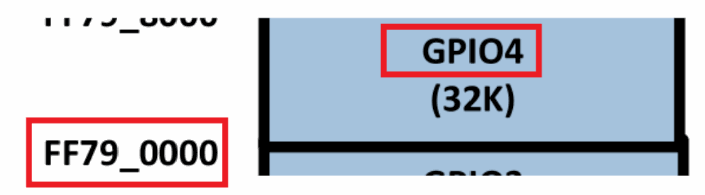
Technical figure from the Chinese source, PDF p.31.
| Module | Base | Size |
|---|---|---|
| GPIO4 | FF79_0000 | 32K |
Query GPIO4 state with the io command:
console:/ # io -4 -l 0x100 0xFF790000
ff790000: 42000000 6a400000 00000000 00000000
ff790010: 00000000 00000000 00000000 00000000
ff790020: 00000000 00000000 00000000 00000000
ff790030: ffffffff ffffffff 00000000 00000000
ff790040: 00000000 9434d0f9 00000000 00000000
ff790050: 438b2f06 00000000 00000000 00000000
ff790060: 00000000 00000000 00000000 3230372a
ff790070: 00000000 00000000 00000000 00000000
ff790080: 42000000 6a400000 00000000 00000000
ff790090: 00000000 00000000 00000000 00000000
ff7900a0: 00000000 00000000 00000000 00000000
ff7900b0: ffffffff ffffffff 00000000 00000000
ff7900c0: 00000000 9434d0f9 00000000 00000000
ff7900d0: 438b2f06 00000000 00000000 00000000
ff7900e0: 00000000 00000000 00000000 3230372a
ff7900f0: 00000000 00000000 00000000 00000000
Interpret it using the GPIO register descriptions in the RK3399 TRM. For example, to inspect gpio4b0:
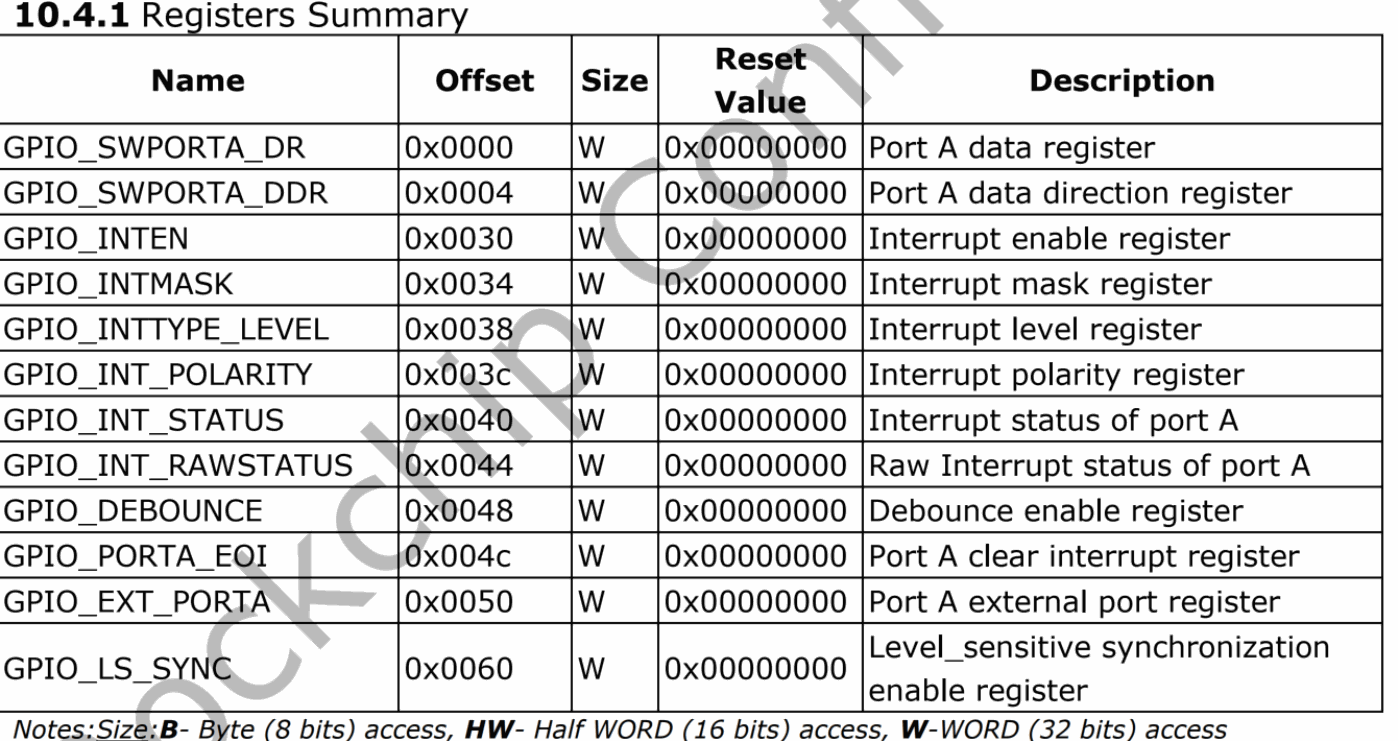
Technical figure from the Chinese source, PDF p.32.
10.4.1 Registers summary
| Name | Offset | Size | Reset Value | Description |
|---|---|---|---|---|
| GPIO_SWPORTA_DR | 0x0000 | W | 0x00000000 | Port A data register |
| GPIO_SWPORTA_DDR | 0x0004 | W | 0x00000000 | Port A data direction register |
| GPIO_INTEN | 0x0030 | W | 0x00000000 | Interrupt enable register |
| GPIO_INTMASK | 0x0034 | W | 0x00000000 | Interrupt mask register |
| GPIO_INTTYPE_LEVEL | 0x0038 | W | 0x00000000 | Interrupt level register |
| GPIO_INT_POLARITY | 0x003c | W | 0x00000000 | Interrupt polarity register |
| GPIO_INT_STATUS | 0x0040 | W | 0x00000000 | Interrupt status of port A |
| GPIO_INT_RAWSTATUS | 0x0044 | W | 0x00000000 | Raw interrupt status of port A |
| GPIO_DEBOUNCE | 0x0048 | W | 0x00000000 | Debounce enable register |
| GPIO_PORTA_EOI | 0x004c | W | 0x00000000 | Port A clear interrupt register |
| GPIO_EXT_PORTA | 0x0050 | W | 0x00000000 | Port A external port register |
| GPIO_LS_SYNC | 0x0060 | W | 0x00000000 | Level-sensitive synchronization enable register |
Size: B = Byte (8-bit) access; HW = Half WORD (16-bit) access; W = WORD (32-bit) access.
Offset 0x4 is the direction register and offset 0x0 is the data register. Reading direction register 0xff790004 returns 0x6a400000. Its bits correspond as follows:
| gpio4d | gpio4c | gpio4b | gpio4a |
|---|---|---|---|
| 0x6a | 0x40 | 0x00 | 0x00 |
Each pair of hexadecimal digits converts to eight binary bits, corresponding from right to left to pins 0 through 7. For example, 0x6a becomes 0110 1010, whose bits from right to left represent gpio4d0 through gpio4d7. According to the register description:
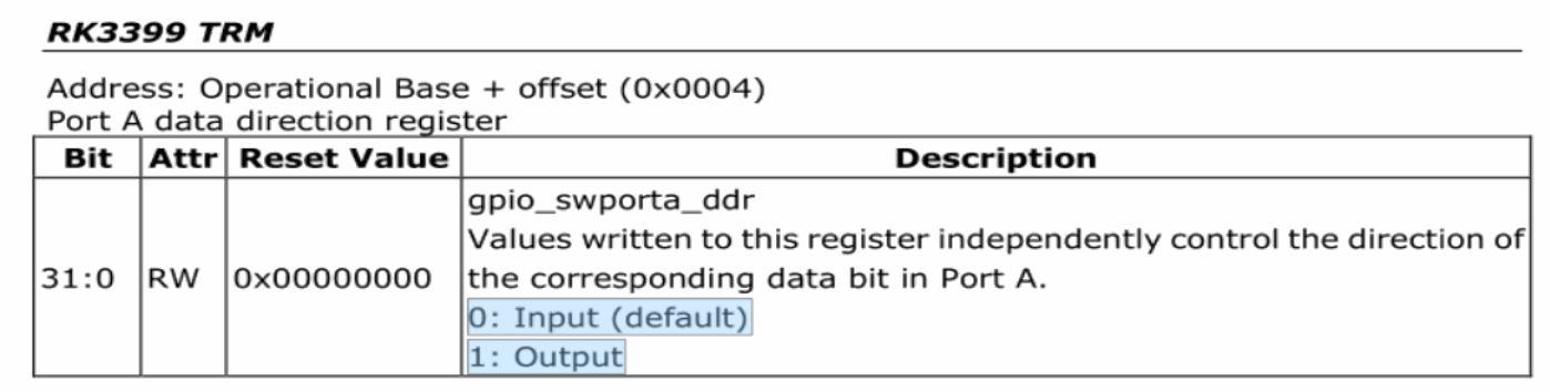
Technical figure from the Chinese source, PDF p.32.
RK3399 TRM — Address: operational base + offset (0x0004). Port A data direction register.
| Bit | Attr | Reset Value | Description |
|---|---|---|---|
| 31:0 | RW | 0x00000000 | gpio_swporta_ddr: values written to this register independently control the direction of the corresponding data bit in Port A. 0: input (default); 1: output. |
gpio4b0 is therefore currently an input. If it were an output, 0xFF790000 would show its high/low level. For input mode, read 0xFF790050 (GPIO_EXT_PORTA) to determine the input level.
8.1.2 IO tool in U-Boot
Hold ctrl + c during U-Boot startup to enter the command line. U-Boot provides numerous commands; enter ? to list those currently supported:
=> ?
? - alias for 'help'
android_print_hdr- print android image header
base - print or set address offset
bdinfo - print Board Info structure
bidram_dump- Dump bidram layout
boot - boot default, i.e., run 'bootcmd'
……
iomem - Show iomem data by device compatible(high priority) or node name
……
md - memory display
……
For earlier versions, use the following configuration, rebuild U-Boot and download it:
Enable the following macro to use IO commands:
diff --git a/include/configs/rk_default_config.h b/include/configs/rk_default_config.h
index 9852917d4f..305de26347 100755
--- a/include/configs/rk_default_config.h
+++ b/include/configs/rk_default_config.h
@@ -304,7 +304,7 @@
/* rk io command tool */
-#undef CONFIG_RK_IO_TOOL
+#define CONFIG_RK_IO_TOOL
U-Boot can also use the md command.
Add the following macro to use md:
diff --git a/include/configs/rk33plat.h b/include/configs/rk33plat.h
index 0906c0c091..3f94e9eabe 100755
--- a/include/configs/rk33plat.h
+++ b/include/configs/rk33plat.h
@@ -140,6 +140,7 @@
#define CONFIG_RK_GPIO_EXT_FUNC
#define CONFIG_CHARGE_LED
#define CONFIG_POWER_FUSB302
+ #define CONFIG_CMD_MEMORY
#endif
#if defined(CONFIG_RKCHIP_RK322XH)
Set bootdelay:
diff --git a/common/autoboot.c b/common/autoboot.c
index c27cc2c751..fe28adb2fd 100644
--- a/common/autoboot.c
+++ b/common/autoboot.c
@@ -146,6 +146,7 @@ static int abortboot_normal(int bootdelay)
{
int abort = 0;
unsigned long ts;
+ bootdelay = 3; //此处添加时间可自由定义,单位:秒
#ifdef CONFIG_MENUPROMPT
printf(CONFIG_MENUPROMPT);
These options are enabled in the default Rockchip configuration. The source recommends md commands for register access. The operations are:
// 读操作
md - memory display
Usage: md [.b, .w, .l, .q] address [# of objects]
// 写操作
mw - memory write (fill)
Usage: mw [.b, .w, .l, .q] address value [count]
Read example: display 0x10 consecutive data items starting at address 0x76000000.
=> md.l 0x76000000 0x10
76000000: fffffffe ffffffff ffffffff ffffffff ................
76000010: ffffffdf ffffffff feffffff ffffffff ................
76000020: ffffffff ffffffff ffffffff ffffffff ................
76000030: ffffffff ffffffff ffffffff ffffffff ................
Write example: assign 0x1234 to address 0x76000000.
=> mw.l 0x76000000 0xffff1234 // 高16位有mask
=> md.l 0x76000000 0x10 // 回读
76000000: ffff1234 ffffffff ffffffff ffffffff ................
76000010: ffffffdf ffffffff feffffff ffffffff ................
76000020: ffffffff ffffffff ffffffff ffffffff ................
76000030: ffffffff ffffffff ffffffff ffffffff ................
8.2 IOMUX tool
iomux is a GCC-compiled binary that obtains and sets GPIO pins through ioctl calls to the rockchip-pinctrl device. It is disabled by default; set CONFIG_ROCKCHIP_IOMUX=y in defconfig.
iomux tool source:
kernel/tools/testing/selftests/rkpinctrl/iomux.c
Build method:
gcc kernel/tools/testing/selftests/rkpinctrl/iomux.c -o iomux
Usage:
Example: set GPIO0_B7 to func1.
[root@RK3588:/]# iomux 0 15 1
Example: get GPIO0_B7 iomux.
[root@RK3588:/]# iomux 0 15
mux get (GPIO0-15) = 1
8.3 Pinconfig tool
PinConfig provides hardware and software engineers with unified IO configuration and verification. Supported chips in the source are RK3588, RK3566, RK3568, RV1126 and RV1109.
For detailed instructions, see PinConfig_UserManual.pdf supplied with the tool.
8.4 PinDebug tool
PinDebug is a pin-debugging tool for querying iomux and configuring pin properties. Supported chips in the source are RK3588, RK3566, RK3568, RV1126, RV1109, RV1106, RV1103 and RK3528.
For detailed instructions, see PinDebug_UserManual.pdf supplied with the tool.
9. GPIO troubleshooting procedure
This chapter gives the basic GPIO troubleshooting procedure. Follow these steps when GPIO input or output cannot be controlled.
9.1 Verify the power supply
Measure the supply voltage of the GPIO power-domain pins. Is it normal and consistent with the schematic? Is the DTS io-domain configuration correct? The most direct check is to read io-domain registers with io. For power-domain configuration, see the IO-Domain chapter.
9.2 Verify IO multiplexing
Most GPIO control failures occur because the pin is multiplexed to another function. Use the GPIO debugging tools, usually io to read the multiplexing register directly; see the debugging-tools chapter. A preliminary check can also be made using the temporary DTS file.
9.3 Verify GPIO clock state
For example, reading GPIO4 registers with the IO tool may return:
ff790000: 42400000 42400000 42400000 42400000
ff790010: 42400000 42400000 42400000 42400000
ff790020: 42400000 42400000 42400000 42400000
ff790030: 42400000 42400000 42400000 42400000
ff790040: 42400000 42400000 42400000 42400000
ff790050: 42400000 42400000 42400000 42400000
ff790060: 42400000 42400000 42400000 42400000
ff790070: 42400000 42400000 42400000 42400000
ff790080: 42400000 42400000 42400000 42400000
ff790090: 42400000 42400000 42400000 42400000
ff7900a0: 42400000 42400000 42400000 42400000
ff7900b0: 42400000 42400000 42400000 42400000
ff7900c0: 42400000 42400000 42400000 42400000
ff7900d0: 42400000 42400000 42400000 42400000
ff7900e0: 42400000 42400000 42400000 42400000
ff7900f0: 42400000 42400000 42400000 42400000
All values in the result are suspiciously identical. If some or all values read by io are the same unusual value, the GPIO clock is disabled and reads/writes are unavailable. Enable the RK3399 GPIO4 clock; search the RK3399 TRM for gpio4_en:
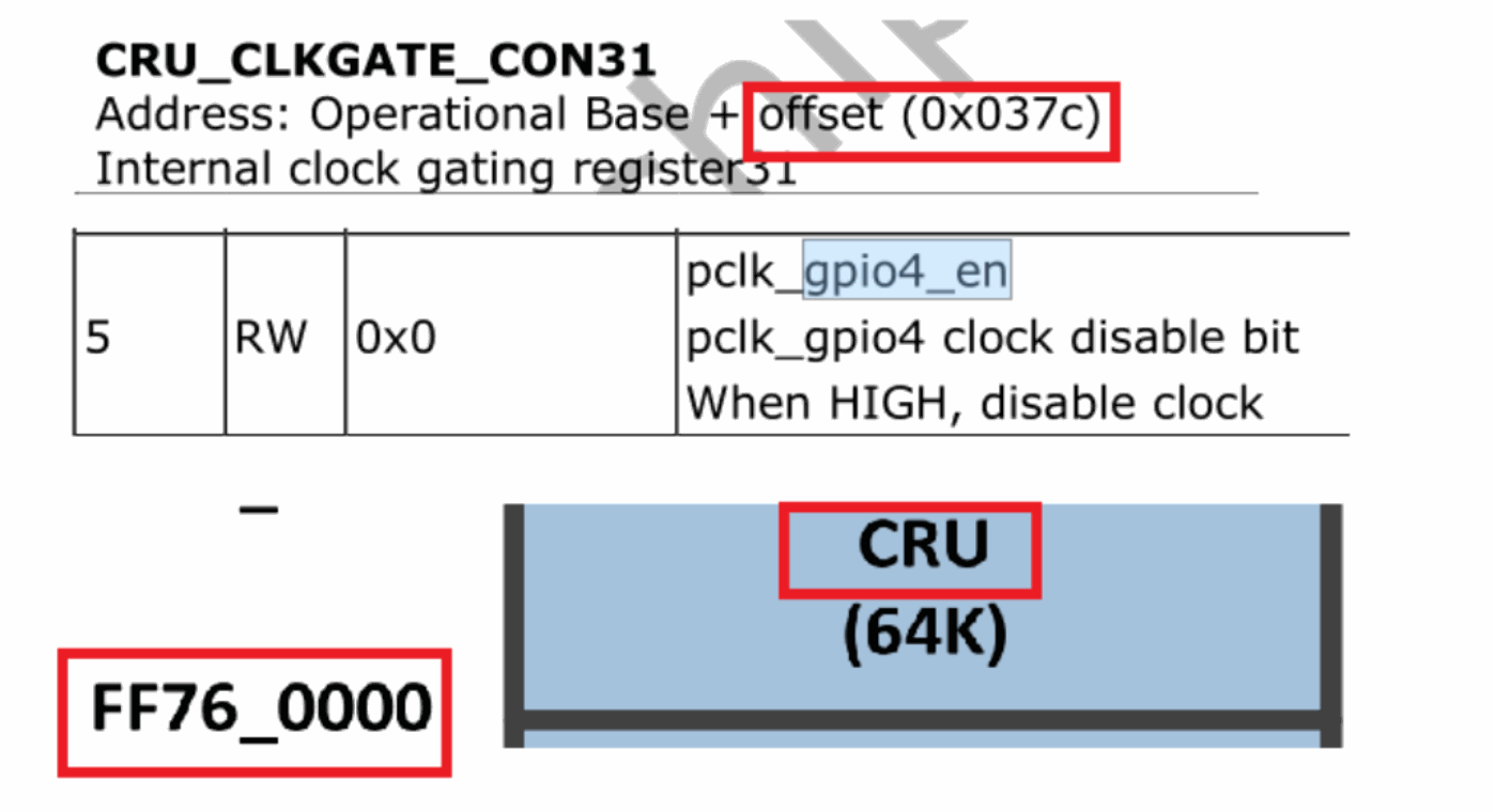
Technical figure from the Chinese source, PDF p.36.
CRU_CLKGATE_CON31 — Address: operational base + offset (0x037c). Internal clock-gating register 31. CRU base FF76_0000, size 64K.
| Bit | Attr | Reset Value | Description |
|---|---|---|---|
| 5 | RW | 0x0 | pclk_gpio4_en: pclk_gpio4 clock-disable bit. When HIGH, disable the clock. |
First read the current GPIO4 clock state using io. A high register bit means disabled:
io -4 -l 0x100 0xFF76037C
ff76037c: 000001b8 00000010 00000000 0000002a
ff76038c: 00000000 00000000 00000000 00000000
ff76039c: 00000000 00000000 00000000 00000000
ff7603ac: 00000000 00000000 00000000 00000000
ff7603bc: 00000000 00000000 00000000 00000000
ff7603cc: 00000000 00000000 00000000 00000000
ff7603dc: 00000000 00000000 00000000 00000000
ff7603ec: 00000000 00000000 00000000 00000000
ff7603fc: 00000000 00000000 000 00000 00000000
ff76040c: 00000000 00000000 00000000 00000000
ff76041c: 00000000 00000000 00004040 00000000
ff76042c: 00000014 00000000 00000000 00000000
ff76043c: 00000000 00000000 00000000 00000000
ff76044c: 00000000 00000000 00000000 00000000
ff76045c: 00000000 00000000 00000000 00000000
ff76046c: 00000000 00000000 00000000 00000000
The result 0x000001b8 is binary 0001 1011 1000. GPIO4’s clock corresponds to bit 5, counted from the right; that bit is 1, meaning disabled. Enable it to allow normal io reads and writes:
io -4 -w 0xFF76037C 0x00200000
io -4 -l 0x100 0xFF790000
ff790000: 42000000 6a400000 00000000 00000000
ff790010: 00000000 00000000 00000000 00000000
ff790020: 00000000 00000000 00000000 00000000
ff790030: ffffffff ffffffff 00000000 00000000
ff790040: 00000000 9434d0f9 00000000 00000000
ff790050: 438b2f06 00000000 00000000 00000000
ff790060: 00000000 00000000 00000000 3230372a
ff790070: 00000000 00000000 00000000 00000000
ff790080: 42000000 6a400000 00000000 00000000
ff790090: 00000000 00000000 00000000 00000000
ff7900a0: 00000000 00000000 00000000 00000000
ff7900b0: ffffffff ffffffff 00000000 00000000
ff7900c0: 00000000 9434d0f9 00000000 00000000
ff7900d0: 438b2f06 00000000 00000000 00000000
ff7900e0: 00000000 00000000 00000000 3230372a
ff7900f0: 00000000 00000000 00000000 00000000
Besides writing registers, the clock can be enabled through the sys interface, for example:
console:sys/kernel/debug/clk # cat clk_summary | grep gpio3
pclk_gpio3 0 1 0 100000000 0 0 50000
console:sys/kernel/debug/clk # ls pclk_gpio3
pclk_gpio3/clk_accuracy pclk_gpio3/clk_parent
pclk_gpio3/clk_available_parent pclk_gpio3/clk_phase
pclk_gpio3/clk_duty_cycle pclk_gpio3/clk_prepare_count
pclk_gpio3/clk_enable_count pclk_gpio3/clk_protect_count
pclk_gpio3/clk_flags pclk_gpio3/clk_rate
pclk_gpio3/clk_notifier_count
console:sys/kernel/debug/clk # echo 1 > pclk_gpio3/clk_enable_count
console:sys/kernel/debug/clk # cat clk_summary | grep gpio3
    pclk_gpio3 1 2 0 100000000 0 0 50000
Note: whether the GPIO clock is enabled depends on whether the GPIO is active, such as during an interrupt or data transfer; it is not directly determined by configuration or API calls.
9.4 Check conflicts caused by other GPIO drivers
If a pin intended as GPIO has correct multiplexing and power-domain settings but the oscilloscope waveform does not follow the high/low transitions in your driver, another driver may be operating it. Add debugging output in gpio_direction_output and gpio_direction_input as below to print all GPIO operations.
drivers/gpio/gpiolib.c
int gpiod_direction_input(struct gpio_desc *desc)
{
    + pr_info("%s: %d\n", __func__, desc_to_gpio(desc));
    ......
}
int gpiod_direction_output(struct gpio_desc *desc, int value)
{
    + pr_info("%s: %d\n", __func__, desc_to_gpio(desc));
    ......
}
To investigate uncontrollable behavior of RK3588 gpio4b3, first use this command to determine the base pin number of gpio4a0:
root@rk3588-buildroot:/# cat /sys/kernel/debug/gpio
gpiochip0: GPIOs 0-31, parent: platform/fd8a0000.gpio, gpio0:
 gpio-26 ( |GTP_RST_PORT ) out hi
 gpio-27 ( |GTP_INT_IRQ ) in hi
gpiochip1: GPIOs 32-63, parent: platform/fec20000.gpio, gpio1:
 gpio-41 ( |vcc-mipicsi0-regulat) out lo
 gpio-42 ( |vcc-mipicsi1-regulat) out lo
gpiochip2: GPIOs 64-95, parent: platform/fec30000.gpio, gpio2:
 gpio-76 ( |reset ) out hi ACTIVE LOW
 gpio-77 ( |hdmirx-det ) in hi ACTIVE LOW
 gpio-84 ( |vcc-mipidcphy0-regul) out hi
gpiochip3: GPIOs 96-127, parent: platform/fec40000.gpio, gpio3:
 gpio-96 ( |bt_default_wake_host) in lo
 gpio-113 ( |ircut-open ) out lo
 gpio-115 ( |vcc3v3-pcie30 ) out lo
#gpio4a0的引脚首编号为128
gpiochip4: GPIOs 128-159, parent: platform/fec50000.gpio, gpio4:
 gpio-130 ( |reset ) out hi
 gpio-133 ( |reset ) out hi
 gpio-134 ( |sbu1-dc ) out lo
 gpio-135 ( |sbu2-dc ) out hi
 gpio-136 ( |vcc5v0-host ) out hi
gpio-137 ( |enable ) out lo
gpio-138 ( |enable ) out lo
gpio-152 ( |vbus5v0-typec ) out lo
Calculate the gpio4b3 pin number:
gpio4b3 = 128 + (B-A) * 8 + 3 = 128 + 1 * 8 + 3 = 139
Look for messages containing 139:
root@rk3588-buildroot:/# dmesg | grep "gpiod_direction_output"
[ 1.460212] gpiod_direction_output: 152
[ 1.460291] gpiod_direction_output: 115
[ 1.460391] gpiod_direction_output: 136
......
[ 1.735094] gpiod_direction_output: 133
[ 1.806359] gpiod_direction_output: 139 #有驱动控制了gpio4b3
[ 2.136271] gpiod_direction_output: 113
9.5 Verify GPIO registers
If the IO power domain and IO reset are confirmed correct, directly read/write GPIO registers with io to determine finally whether software configuration is responsible.
Check these three GPIO registers:
Port Data Register: GPIO output register (Low/High)
Port Data Direction Register: GPIO direction register (Input/Output)
External Port Data Register: actual GPIO external-port level (Low/High)
For example, when GPIO is configured high, if the output register is 1 and the direction register is 1 but the external-port level is 0, the cause is most likely hardware: external circuitry is pulling the GPIO low.
10. FAQ
10.1 Output level cannot be controlled at power-on
Software cannot control the level immediately at power-on. Select a GPIO whose default hardware state has the required pull-up or pull-down. Using RK3399 gpio2c2 without external circuitry as an example, confirm the default state in the datasheet or by the suffix in the schematic pin name:
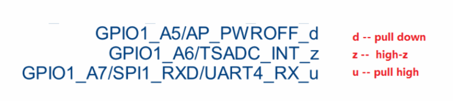
Technical figure from the Chinese source, PDF p.39.
For a high level at power-on, select a GPIO pin with the -u suffix; for a low level, select one with -d.
Some pins are not GPIO by default. Check the reset value of the multiplexing register in the TRM; JTAG pins, for example, default to JTAG mode.
10.2 Spurious GPIO interrupts
For spurious GPIO interrupts, enable Schmitt-trigger mode by configuring the GPIO as pcfg_pull_none_smt.
10.3 RV1103/RV1106 gpio3b0~gpio3c3 cannot be controlled
RV1103/RV1106 gpio3b0~gpio3c3 are special: GPIO mode requires additional register configuration, and they can only be inputs. GPIO and MIPI modes for this group are mutually exclusive. Follow these steps:
io -4 0xFF3B4804 0x40000000 #使能gpio3b的clk
io -4 0xFF3B4808 0x00100000 #使能gpio3c的clk
io -4 0xFF3E8000 0x7D #Clk/data lane enable
io -4 0xFF3E8080 0x5F #MIPI/LVDS enable
# 如果引脚是gpio3b6~gpio3b7和gpio3c0~gpio3c,则配置0xFF3E844C寄存器
io -4 0xFF3E844C 0x00010001 #切换csi_dphy_path0为TLL_MODE
# 如果引脚是gpio3b0~gpio3b5,则配置0xFF3E884C寄存器
io -4 0xFF3E884C 0x00010001 #切换csi_dphy_path1为TLL_MODE
io -4 0xFF55804c 0x00070000 #设置GPIO3_B4复用寄存器
10.4 RV1108 gpio1a0~gpio1b1 cannot be controlled
The source text refers here to RV1108 gpio3b0~gpio3c3. To configure them as GPIO, set DPHY_LVDS_TTL to TTL mode as follows:
io -4 0x2022838C 0x00000004 #enable TTL mode,disable LVDS mode,disable mipi mode
io -4 0x202283AC 0x000000fd #disable Data Lane,disable Clock Lane
10.5 RK3588 gpio4d2 and gpio4d3 cannot be controlled
For RK3588, and for other platforms such as RK3576 with the same issue, consult force_jtag in the manual before selecting GPIO mode:
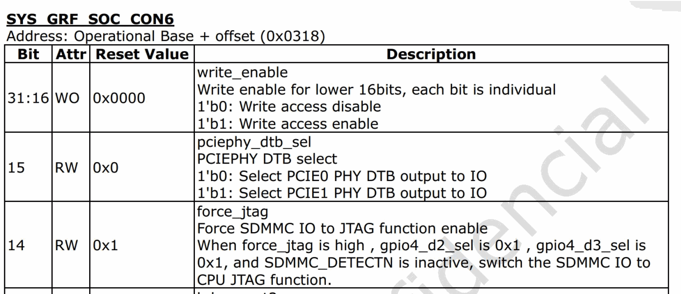
Technical figure from the Chinese source, PDF p.41.
SYS_GRF_SOC_CON6 — Address: operational base + offset (0x0318).
| Bit | Attr | Reset Value | Description |
|---|---|---|---|
| 31:16 | WO | 0x0000 | write_enable: individual write enable for each of the lower 16 bits. 1’b0: write access disabled; 1’b1: write access enabled. |
| 15 | RW | 0x0 | pciephy_dtb_sel: PCIEPHY DTB selection. 1’b0: select PCIE0 PHY DTB output to IO; 1’b1: select PCIE1 PHY DTB output to IO. |
| 14 | RW | 0x1 | force_jtag: enable forcing SDMMC IO to JTAG. When force_jtag is high, gpio4_d2_sel is 0x1, gpio4_d3_sel is 0x1, and SDMMC_DETECTN is inactive, switch SDMMC IO to the CPU JTAG function. |
Clear the default force_jtag bit:
io -4 0xFD58C318 0x40000000 #disable force_jtag
io -4 0xFD5F8098 0x0F000000 #iomux set to gpio
10.6 /sys/class/gpio is missing from the Android SDK
In device/rockchip/rk3588/BoardConfig.mk set BOARD_BUILD_GKI := false, and enable CONFIG_DEBUG_GPIO and CONFIG_GPIO_SYSFS in the kernel configuration.
10.7 Incorrect GPIO level readback
1. Is IOMUX configured as GPIO?
2. Is the GPIO DDR register configured for input?
3. Is the GPIO clock enabled?
4. Does GPIO have an internal/external pull-up?
5. Read GPIO_EXT_PORT to check the GPIO level. This register reflects the actual pin level, so IOMUX and DDR must be configured correctly and the pulls must not leave a high-impedance state.
10.8 Binding a GPIO interrupt to a specific core
The following patch changes interrupt affinity to CPU2:
--- a/drivers/gpio/gpio-rockchip.c
+++ b/drivers/gpio/gpio-rockchip.c
@@ -579,6 +579,25 @@ static int rockchip_interrupts_register(struct rockchip_pin_bank *bank)
        irq_set_chained_handler_and_data(bank->irq,
                                         rockchip_irq_demux, bank);
+ // +++ 新增:设置中断亲和性到CPU2 +++
+ {
+ struct cpumask cpumask;
+ int cpu = 2; // 指定CPU2
+
+ // 检查CPU2是否有效
+ if (cpu < num_possible_cpus()) {
+ cpumask_clear(&cpumask);
+ cpumask_set_cpu(cpu, &cpumask);
+ if (irq_set_affinity_hint(bank->irq, &cpumask)) {
+ dev_warn(bank->dev, "Failed to set IRQ affinity for CPU%d\n", cpu);
+ } else {
+ dev_warn(bank->dev, "IRQ%d affinity set to CPU%d\n", bank->irq, cpu);
+ }
+ } else {
+ dev_warn(bank->dev, "Invalid CPU%d for IRQ affinity\n", cpu);
+ }
+ }
+
        return 0;
 }
10.9 GPIO interrupt response latency
1. Change interrupt affinity.
2. CONFIG_HZ=1000 // Change the timer tick interval
- A high HZ value, such as 1000: a timer interrupt occurs every 1ms, and the scheduler has at most 1ms delay before responding to a new task.
- A low HZ value, such as 100: an interrupt occurs every 10ms, and task-switch latency may reach 10ms.
3. Increase the CPU frequency.
4. Apply a real-time patch following the documentation in docs\Patches\Real-Time-Performance.