
This is a source-based hardware design topic for platform reference; no corresponding ArmSoM board is confirmed. Parameters are source references, not ArmSoM measurements. Check silicon revision, PCB, SDK/BSP, kernel, firmware and peripheral specifications before implementation.
Design V1.0 §1.1–1.4, §2.1–2.3, §2.11; PDF 5–9, 14–15, 19
From BROM to the operating system
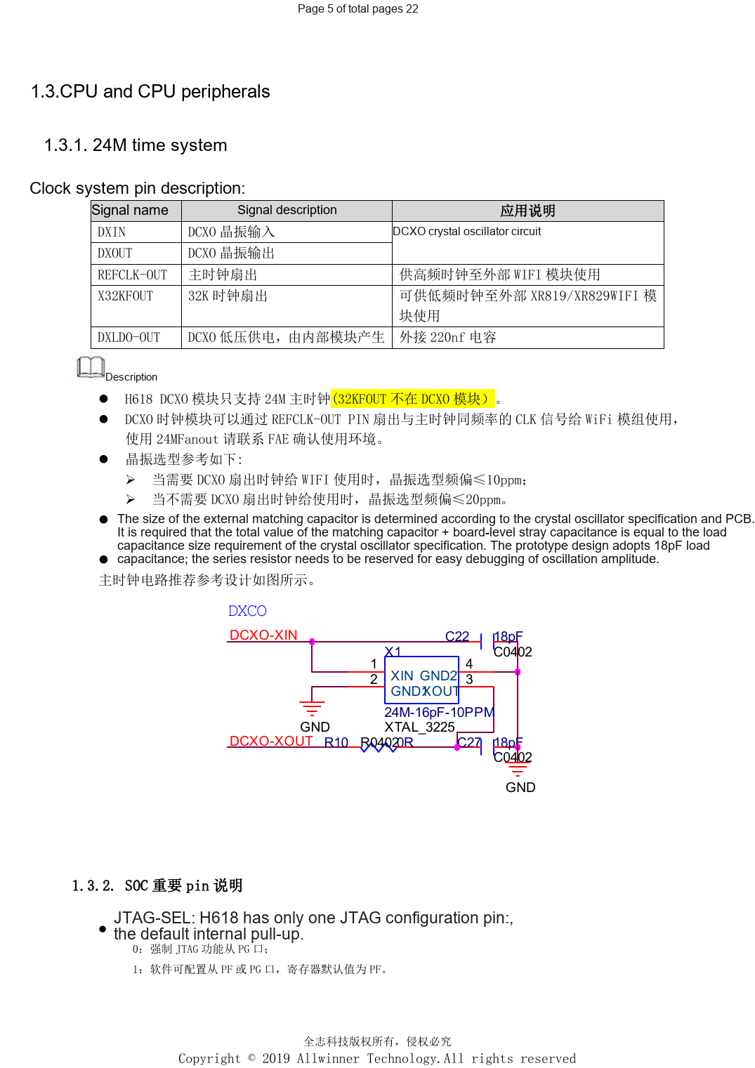
After reset, BROM initializes power, clocks, buses, reset and storage. Initialization information for UART and DRAM is read into SRAM, followed by Boot0, U-Boot and the operating system with its peripherals. Accessible serial diagnostics, boot straps and recovery belong in the minimum system. JTAG-SEL has an internal pull-up: low forces PG; high allows software selection of PF/PG, defaulting to PF. Pull AP-RESET up to VCC-PLL and retain its RC and ESD protection.
Power and sequencing
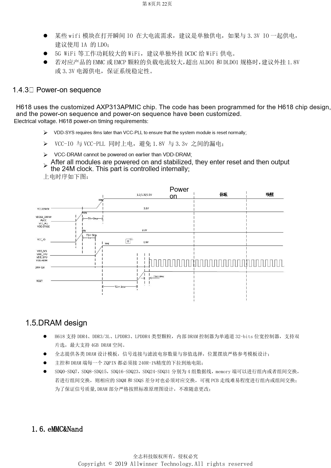
The reference uses a preprogrammed AXP313A. VDD-SYS follows VCC-PLL by 8ms; VCC-IO rises with VCC-PLL, and VCC-DRAM must not precede VDD-DRAM. Internal reset and the 24MHz clock follow stable supplies. CPU power is separate for DVFS; GPU and SYS share a rail that must not be independently voltage-scaled. The reference uses 22µF at the CPU regulator and load, two 22µF near SYS/GPU and at least 10µF near VCC-DRAM. Assess separate supplies for high-power Wi-Fi or eMMC loads exceeding the LDO rating.
Clock and source inconsistencies
DCXO supports only 24MHz. Crystal tolerance is ≤10ppm with Wi-Fi fanout and ≤20ppm otherwise. Fit 220nF on DXLDO-OUT. The 18pF capacitors are prototype examples, not universal values; keep DXIN/DXOUT below 400mil with ground shielding. The source lists 1.6A SYS+GPU load against 1.5A PMU capability: this requires clarification, not a claim of headroom. Its contents page says V2.1 while the cover and revision record say V1.0; this series identifies the source as V1.0.
Parameter reference
| Item | Source reference |
|---|---|
| Boot medium; PC3/4/5/6 | MLC NAND / SLC NAND: 1/1/1/1; eMMC USER: 0/1/1/1; eMMC BOOT: 1/0/1/1; SPI_NOR: 1/1/0/1; SPI_NAND: 1/1/1/0 |
| Module supply minimum | >=1.78V; nominal 1.8V ±1% |
Reference figures
These reference-page captures retain the original Chinese figure labels. No matching English edition was found; all four languages use the Chinese originals. Text parameters and steps remain copyable; captures support checking. Page numbers are physical PDF pages.
Choosing an ArmSoM platform
For an ArmSoM project, select a platform through official products and documentation, then verify processor, interfaces and software support anew. A733/H618 circuits are not transferred to another SoC by assumption.
Series reading
- H618 DDR and eMMC: templates, impedance and PCB review
- H618 interfaces: USB, HDMI, Ethernet and ESD layout
- H618 bring-up and stability: flashing, DDR and fault isolation
- H618 · Series index
Appendix: source AXP313A supply table
Design V1.0 · PDF 8
CPU/SYS use “+5%”, not “±5%”, in the source; the sign is not silently corrected. See the SYS+GPU current conflict above. The DRAM value is a DDR3 example, not universal.
| Rail | Voltage | Accuracy (source) | Ripple/noise | Scenario peak | PMU capacity |
|---|---|---|---|---|---|
| CPU | 0.9V | 0.9V+5% | <90mV | 1.8A | 3A |
| SYS+GPU | 0.94V | 0.94V+5% | <90mV | 1.6A | 1.5A |
| DRAM | 1.5V | 1.5V±10% | <125mV | 1A | 2A |
| Module | 1.8V | 1.8V±1% | <30mV | 100mA | 300mA |
| IO normal | 3.3V | 3.3V±10% | <125mV | 200mA | 500mA |