
This is a source-based hardware design topic for platform reference; no corresponding ArmSoM board is confirmed. Parameters are source references, not ArmSoM measurements. Check silicon revision, PCB, SDK/BSP, kernel, firmware and peripheral specifications before implementation.
Design V1.0 §1.7–1.13, §2.6–2.15; PDF 10–13, 17–21; PCB checklist V1.0
USB and display interfaces
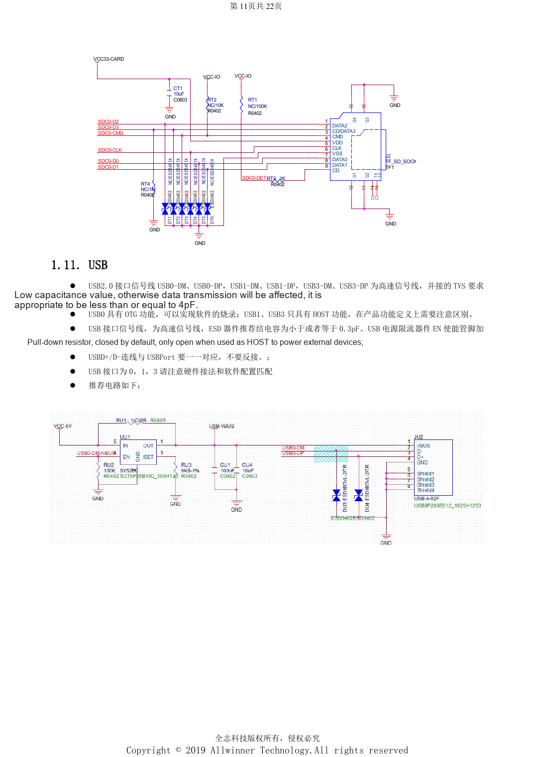
USB0 supports OTG/flashing; USB1 and USB3 are hosts. Port number 3 does not mean USB3.0. Pull the current-limit enable low by default and activate it only for host power. The same source page specifies both ≤4pF and ≤0.3pF for TVS capacitance; clarify the intended nets rather than choosing an arbitrary universal limit. HDMI includes IIC/CEC level shifting; use a low-drop Schottky on 5V to prevent backfeed and avoid falling below 4.75V. CVBS is a current output using an 0805 75Ω shunt and ground-shielded routing.
Networking, Wi-Fi and audio
Ethernet high-voltage capacitors are at least 1206 and 2kV, with 0805 75Ω resistors; prohibit traces and copper beneath the transformer. The guide requires >50mil high/low-voltage separation while the checklist says at least 2mm: retain the stricter review item and check the enclosure. Match Wi-Fi IO to PG; the SDIO clock reference is 33Ω plus 5.6pF. Bluetooth wake requires an appropriate always-on supply. RF is 50Ω, preferably <6cm, >3mm from the edge, without branches or layer changes, with ground vias every 0.5–1mm. Audio AVCC is ≥25mil; VRA1/2 ≥10mil and ≤300mil; separate LINEOUT from DDR noise.
Review ESD and thermal paths together
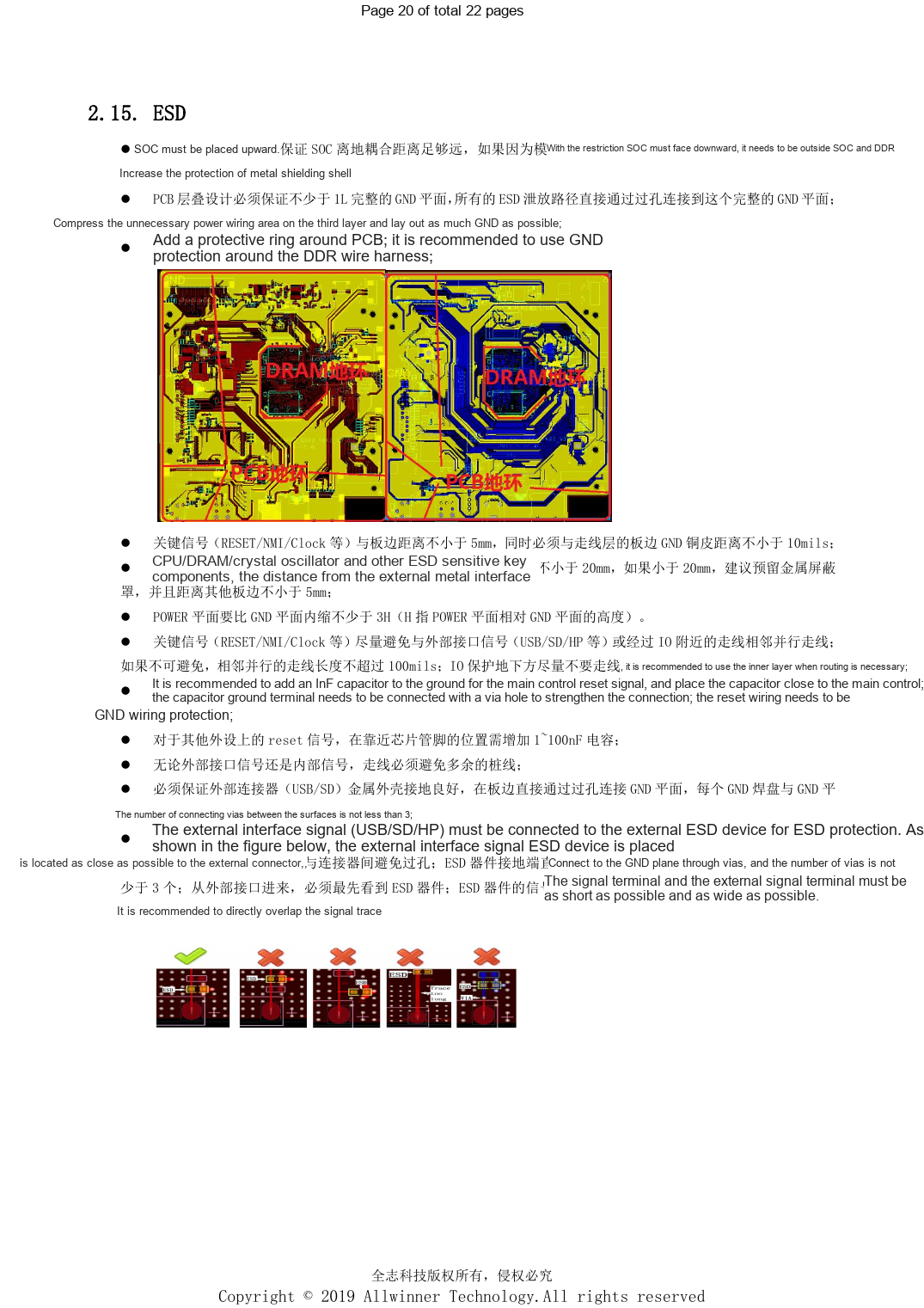
Keep at least one continuous ground layer. Place protection at the connector, ahead of the internal circuit, with at least three ground vias. RESET/NMI/Clock stay ≥5mm from the edge and ≥10mil from edge ground copper; CPU/DDR/crystals stay ≥20mm from exposed metal ports, otherwise consider shielding. SoC reset uses a 1nF reference; peripheral reset uses 1–100nF, not interchangeable rules. Recess power planes by at least 3H relative to ground. Central thermal vias reference 10–12mil holes and 30–40mil pitch; distribute heat sources and use the >2cm PMU/SoC reference spacing. Whole-product thermal and EMC tests remain necessary.
Parameter reference
| Item | Source reference |
|---|---|
| USB routing | 90Ω; length <4000mil; vias ≤2; clearance >10mil |
| HDMI routing | 90–100Ω; intra-pair <10mil; inter-pair <100mil; length <3000mil |
| SD Card routing | 50Ω; data-to-CLK <500mil; CLK resistor within 300mil of SoC |
Reference figures
These reference-page captures retain the original Chinese figure labels. No matching English edition was found; all four languages use the Chinese originals. Text parameters and steps remain copyable; captures support checking. Page numbers are physical PDF pages.
Choosing an ArmSoM platform
For an ArmSoM project, select a platform through official products and documentation, then verify processor, interfaces and software support anew. A733/H618 circuits are not transferred to another SoC by assumption.