
This ArmSoM platform reference describes the RK3588S chip, not a board compatibility claim. Verify the exact device, schematic, power rails and BSP. Figures and performance data are Rockchip reference material; no ArmSoM hardware tests were performed. No SDK or kernel version is specified.
Sources: two byte-identical English RK3588S Rev1.5 PDFs, 2023-01-17, each35 pages, in CN and EN directories. Electrical and thermal chapter headers say Rev1.2. All figures are English originals.
1.1
RK3588S is a low-power, high-performance processor for ARM-based PCs, edge-computing devices, personal mobile Internet devices and other digital multimedia applications. It integrates four Cortex-A76 cores and four Cortex-A55 cores, each with a NEON coprocessor. Hardware engines accelerate demanding applications. Video decoding supports H.265 and VP9 at 8K@60fps, H.264 at 8K@30fps, and AV1 at 4K@60fps. H.264 and H.265 encoding supports 8K@30fps; high-quality JPEG encoding/decoding and dedicated image preprocessing and postprocessing are also integrated. The 3D GPU supports OpenGLES 1.1, 2.0 and 3.2, OpenCL up to 2.2, and Vulkan 1.2. A dedicated 2D engine with an MMU accelerates display operations. The fully hardware-based ISP supports up to 48 megapixels and accelerates HDR, 3A, LSC, 3DNR, 2DNR, sharpening, dehaze, fisheye correction and gamma correction. The NPU supports mixed INT4/INT8/INT16/FP16 operations and up to 6 TOPS; models from TensorFlow, MXNet, PyTorch and Caffe can be converted. The four-channel external memory interface supports LPDDR4/LPDDR4X/LPDDR5 and demanding bandwidth requirements. A comprehensive peripheral interface set supports flexible applications.
1.2.1
Microprocessor. Four ARM Cortex-A76 MPCore and four ARM Cortex-A55 MPCore application processors combine high performance, low power and caches. DSU (DynamIQ Shared Unit) contains the L3 memory system, control logic and external interfaces for the DynamIQ cluster. The ARMv8-A instruction set is fully implemented, including ARM NEON Advanced SIMD for media/signal processing and ARMv8 Cryptography Extensions; TrustZone is supported. Each A76 has 64KB L1 instruction, 64KB L1 data and 512KB L2 cache; each A55 has 32KB L1 instruction, 32KB L1 data and 128KB L2 cache. All eight cores share 3MB L3. Eight independent power domains support internal power switches and externally controlled on/off operation for different applications: PD_CPU_0/1/2/3 correspond respectively to A55 cores 1/2/3/4, and PD_CPU_4/5/6/7 to A76 cores 1/2/3/4; each includes NEON, FPU and L1/L2 instruction/data caches. Three separate voltage domains support DVFS: A76_0+A76_1, A76_2+A76_3, and DSU+Cortex-A55.
1.2.2
Memory organization. On-chip BootROM boots through SPI, eMMC or SD/MMC and downloads system code through USB OTG. Shared memory is in VD_LOGIC; PMU SRAM in VD_PMU serves low-power applications. External dynamic memory complies with JEDEC LPDDR4/LPDDR4X/LPDDR5, with four 16-bit channels, up to two ranks/chip selects per channel and up to 32GB total address space. SDRAM supports power-down and self-refresh. The eMMC interface fully complies with JEDEC eMMC 5.1/5.0 and is backward-compatible with 4.51 and earlier; HS400, HS200, DDR50 and legacy modes use 1-, 4- or 8-bit buses. SD/MMC supports SD3.0 and MMC 4.51 with a 4-bit bus. FSPI transfers data to/from serial flash using 1-, 2- or 4-bit buses and two chip selects.
1.2.3
System components. Three Cortex-M0 MCUs are integrated: VD_PMU has 16KB cache+16KB TCM, VD_NPU has 16KB cache+64KB TCM, and PD_CENTER has 32KB TCM. Their programmable interrupt controller connects all CPU GIC IRQ lines also to PMU_M0 and DDR_M0; a JTAG debug controller is integrated. CRU generates clocks with 18 PLLs and one 24MHz oscillator input, gates individual components, and supports global and individual software reset. PMU offers configurable operating modes using frequency adjustment, automatic clock gating and power-domain switching, multiple wake sources, 10 separate voltage domains and 45 software-switchable power domains. There are 12 secure and 18 non-secure timers, each with a 64-bit counter, interrupt operation, free-running/user-defined counting and readable working state. Sixteen PWMs (PWM0–PWM15) support interrupts, programmable bus-clock prescaling followed by further division, 32-bit timers/counters, capture, continuous/one-shot and reference modes and variable-duty waveforms. PWM3/7/11/15 are optimized for infrared. Five watchdogs serve CPU/MCU; each 32-bit counter counts a preset value down to zero. Timeout either resets immediately or first interrupts, then resets on a second timeout if software has not cleared it. The interrupt controller accepts 12 PPI and 480 SPI sources and 16 software-triggered interrupts; fixed polarity is high-level for SPI and low-level for PPI, with software-programmable priority per source. Three microcode-programmed DMACs support linked-list scatter/gather and memory-to-memory, memory-to-peripheral and peripheral-to-memory transfers. Each has 8 channels, 32 peripheral hardware requests, 2 interrupt outputs and TrustZone with per-channel programmable security. Two cipher engines support LLI DMA; hardware-padded SHA-1, SHA-256/224, SHA-512/384, MD5 and SM3; hardware-padded HMAC using SHA-1/SHA-256/SHA-512/MD5/SM3; AES-128/192/256 encryption/decryption; AES and SM4 modes ECB/CBC/OFB/CFB/CTR/CTS/XTS/CCM/GCM/CBC-MAC/CMAC; DES/TDES in ECB/CBC/OFB/CFB; RSA/ECC/SM2 PKA operations up to 4096 bits; and random-number generation. Security includes key ladders, scrambling for all DDR types, secure OTP/debug/DFT/OS, and software-selectable secure/non-secure modes for non-CPU masters. Some slaves accept secure masters only, others accept either class as programmed. Part of shared SRAM is secure-only. External DDR divides into 16 regions with programmable access by each master. Three mailboxes connect CPU and MCU; each contains four elements comprising a data word, command-word register and interrupt flag. There are 32 software lock registers indicating occupancy. Hardware decompresses GZIP, LZ4 (general and legacy frame formats), DEFLATE and ZLIB, verifies LZ4 Hash32, and limits decompressed output size to prevent malicious memory destruction.
1.2.4
Video codec. Real-time decoding supports MPEG-1/2/4, H.263, H.264, H.265, VC-1, VP9, VP8, MVC and AV1, with an embedded MMU and parallel multichannel decoding at lower resolutions. The following capability tuples retain the source profile, level, resolution and rate, including the source marker ②. H.265/H.264 real-time encoding supports up to 8K@30fps and parallel multichannel operation at lower resolutions.
| Codec | Format | Resolution | |
|---|---|---|---|
| H.264 AVC/MVC Main10 L6.0 | 8K@30fps | 7680x4320 | ② |
| VP9 Profile0/2 L6.1 | 8K@60fps | 7680x4320 | |
| H.265 HEVC/MVC Main10 L6.1 | 8K@60fps | 7680x4320 | |
| AVS2 Profile0/2 L10.2.6 | 8K@60fps | 7680x4320 | |
| AV1 Main Profile 8/10bit L5.3 | 4K@60fps | 3840x2160 | |
| MPEG-2 MP | 1080p@60fps | 1920x1088 | |
| MPEG-1 MP | 1080p@60fps | 1920x1088 | |
| VC-1 AP level 3 | 1080p@60fps | 1920x1088 | |
| VP8 version2 | 1080p@60fps | 1920x1088 |
1.2.5
JPEG codec. Encoding uses baseline sequential DCT, sizes 96x96–8192x8192 (67Mpixels), up to 90 million pixels/s and four encoder units. Decoding accepts 48x48–65536x65536, YUV400/YUV411/YUV420/YUV422/YUV440/YUV444 and MJPEG, up to 1080P@280fps and 560 million pixels/s. The source also says ‘four encoder units’ under the decoder heading; that wording is retained as a source inconsistency, not silently corrected.
1.2.6
Neural processing unit. The accelerator reaches up to 6 TOPS. Three NPU cores operate together as three, as two, or independently. Supported arithmetic is integer 4/8/16, float16, Bfloat16 and tf32. Internal buffering is 384KBx3. Multiple tasks and scenarios run in parallel. Supported frameworks include TensorFlow, Caffe, Tflite, Pytorch, Onnx NN and Android NN. One separate voltage domain supports DVFS.
1.2.7
Graphics engine. The ARM Mali-G610 MP4 3D engine supports OpenGLES 1.1/2.0/3.2, OpenCL 2.2 and Vulkan 1.2. Four shader cores share a hierarchical tiler; MMU and 4x256KB L2 cache are included. It uses Valhall, AFBC 1.3, Serial Wire debugging for its embedded MCU and a separate DVFS voltage domain. The 2D engine accepts ARGB/RGB888/RGB565/YUV420/YUV422/BPP and outputs ARGB/RGB888/RGB565/YUV420/YUV422; maximum source/destination sizes are 8192x8192/4096x4096. It supports block transfer, transparency, gradient/pattern fills, global and per-pixel alpha (color and alpha channels separately), fading, arbitrary noninteger scaling from 1/8 to 8, rotations 0/90/180/270 degrees, X/Y mirroring with rotation, ROP2/ROP3/ROP4 and 4k/64k-page MMU. The image-enhancement processor accepts planar/semi-planar YUV420/YUV422 with UV swapping; outputs semi-planar YUV420/YUV422 with UV swapping and tile mode; downsamples YUV422 to YUV420; handles moving images up to 1920x1080 and deinterlaces.
1.2.8
Video inputs. Two MIPI DPHY/CPHY combo PHYs each support DPHY1.2 with four lanes at2.5Gbps/lane or CPHY1.1 with three trios at2.5Gsps/trio. Two CSI DPHY1.2 interfaces offer two lanes each at2.5Gbps/lane; pairs combine into four lanes. Camera combinations: two DCPHY plus two two-lane CSI DPHY supports four cameras; two DCPHY plus one four-lane CSI DPHY supports three. One standard8/10/12/16-bit DVP accepts up to150MHz, BT.601/BT.656/BT.1120, with configurable pixel_clk/hsync/vsync polarity.
1.2.9
Image signal processor. VICAP supports BT601/BT656/BT1120 and six MIPI CSI/DSI interfaces with up to four IDs each; CSI formats RAW8/10/12/14 and YUV422; HDR virtual-channel, identification-code and line-counter modes; and RAW pass-through to ISP0/1. Maximum input is 48M 8064x6048@15 with dual ISP, 32M 6528x4898@30 with dual ISP, or 16M 4672x3504@30 with one ISP. Processing includes 3A statistics (AE/histogram, AF, AWB), FPN fixed-pattern-noise removal, BLC black-level correction, DPCC static/dynamic defective-pixel-cluster correction, PDAF phase-detection autofocus, LSC lens shading, Bayer-2DNR spatial/Bayer-3DNR temporal raw denoising, CAC chromatic-aberration correction, three-frame HDR merging, DRC dynamic-range compression/tone mapping, GIC green-imbalance correction, advanced adaptive Debayer with chromatic-aberration correction, CCM/CSM color matrices and RGB2YUV, output gamma correction, automatic dehaze/effect enhancement, customer 3DLUT palette, horizontal-only LDCH lens-distortion correction, YUV-2DNR spatial denoising, sharpening and boundary filtering, CMSK privacy masking, local GAIN and ISP reuse by multiple sensors. Fisheye correction accepts RASTER YUV422SP/YUV422I/YUV420SP and outputs the same RASTER formats or FBCE YUV422SP/YUV420SP. Grid densities are 16x8 or 32x16, reduction factor up to 4, resolution 128x128–4095x4095, bicubic Y and bilinear C interpolation.
1.2.10
Display interfaces. One HDMI/eDP TX combo interface support x1/x2/x4, but HDMI and eDP cannot operate simultaneously on the same interface. HDMI FRL rates: 3/6/8/10/12Gbps; eDP: 1.62/2.7/5.4Gbps. HDMI reaches 7680x4320@60Hz, eDP 4K@60Hz. HDMI supports RGB/YUV up to 10 bits, DSC1.2a and HDCP2.3; eDP supports RGB/YCbCr4:4:4/YCbCr4:2:2, 8/10 bits per component and HDCP1.3. One DP TX1.4a interface combine with USB3.1 Gen1 and support 1/2/4 lanes, 1.62/2.7/5.4/8.1Gbps serializers, up to 7680x4320@30Hz, RGB/YUV up to 10 bits, SST, Type-C DP Alt Mode and HDCP2.3/1.3. Two MIPI interfaces support DPHY2.0 with 4 lanes at up to 4.5Gbps/lane or CPHY1.1 with 3 trios at up to 2.0Gsps/trio, up to 4K@60Hz, left/right dual-display mode, RGB up to 10 bits and DSC1.1/1.2a. BT.1120 output supports 1920x1080@60Hz and up to 150MHz. BT.1120 additionally supports RGB up to8bit.
1.2.11
Video output processor. Maximum outputs: Video Port0 7680x4320@60Hz; Port1 and Port2 each 4096x4320@60Hz; Port3 2048x1080@60Hz. Cluster0/1/2/3 each support 4096x4320 input/output, AFBCD, RGB/YUV/YUYV, scaling 4–1/4 and rotation. ESMART0/1/2/3 each support 4096x4320 input/output, RGB/YUV/YUYV, scaling 8–1/8 and four regions. Overlay combines up to eight layers (four clusters+four ESMART) in RGB or YUV. Postprocessing supports HDR10/HLG, HDR2SDR/SDR2HDR and 3D-LUT/P2I/CSC/BCSH/DITHER/CABC/GAMMA/COLORBAR. Writeback uses ARGB8888/RGB888/RGB565/YUV420 up to 1920x1080.
1.2.12
Audio interfaces. I2S0/I2S1 support up to 8 TX and 8 RX channels. Both use 16–32-bit resolution, up to 192kHz, software-selectable master/slave, I2S normal/left-/right-justified, PCM early/late1/late2/late3 and TDM normal, half-cycle/one-cycle/two-cycle left shift or right shift. I2S/PCM/TDM cannot operate simultaneously. I2S2/I2S3 each support 2 TX and 2 RX channels, 16–32 bits, up to 192kHz, programmable master/slave, the same three I2S and four PCM formats; I2S and PCM cannot run simultaneously. SPDIF0/1 pack two 16-bit samples into one 32-bit location, output biphase stereo, align 16–31-bit data left/right in 32-bit buffers, transfer linear PCM at 16/20/24 bits and support nonlinear PCM. PDM0/1 offer up to 8 channels, 16–24-bit resolution, up to 192kHz and master receive mode. The digital audio codec has two digital DAC channels, I2S/PCM master/slave, 16-bit sampling, three mixing modes per DAC channel and volume control. VAD reads I2S/PDM voice data, detects amplitude, stores microphone-array data and supports a combined level interrupt.
1.2.13
Connectivity. SDIO supports SDIO3.0 with a 4-bit bus. One GMAC support RGMII at 10/100/1000Mbps and RMII at 10/100Mbps, full or half duplex. USB3.1 Gen1 (equivalent to USB3.2 Gen1 and USB3.0) reaches 5Gbps. One OTG interface, USB3OTG_0, combine with DP TX; one Host interface, USB3OTG_2, combines with PIPE PHY2. Compliance: USB3.0 revision1.0, USB2.0 except USB3OTG_2, and xHCI1.1. Transfers include control, bulk with streams, interrupt and isochronous; simultaneous IN/OUT is supported. Descriptor caching and data prefetch improve high-latency-system performance. Power management supports USB2.0 LPM except on USB3OTG_2 and USB3.1 U0/U1/U2/U3. Device functions provide up to 10 IN and 6 OUT endpoints, each count including control endpoint0; up to 16 transfer resources, one per endpoint; flexible endpoint configuration for applications/USB set-configuration modes; hardware ERDY and burst handling; stream-based bulk endpoints with automatic controller data movement; isochronous endpoints using data buffers; and flexible descriptors supporting buffer-interrupt moderation, multiple transfers, isochronous/control transfers and scattered buffering. xHCI host supports up to 64 devices, one interrupter, one USB2.0 port except USB3OTG_2, one SuperSpeed port and standard/open-source xHCI/class drivers. DRD features include static device/host operation and ID-based USB3.1/USB2.0 OTG A/B operation; USB3OTG_2 supports USB3.1 Gen1 only. SRP, HNP and RSP are not supported. USB2.0 PHY supports battery-charge detection; USB3OTG_0 support Type-C/DP Alt Mode; USB3OTG_2 PHY shares PCIe/SATA. Two USB2.0 hosts comply with USB2.0, support high/full/low speeds 480/12/1.5Mbps and EHCI1.0/OHCI1.0a. Two Combo PIPE PHYs support PCIe2.1/SATA3.0/USB3.1 controllers: PHY0 selects SATA or PCIe2.1; PHY2 selects SATA, PCIe2.1 or USB3.1 Gen1. Each PCIe2.1 interface has one lane at 5Gbps, follows PCI Express Base2.1 and supports Root Complex only. Each SATA interface has one 6Gbps port, supports eSATA and complies with Serial ATA3.1/AHCI1.3.1. Five SPI controllers (SPI0–SPI4) are provided; two chip-select outputs and software-selectable serial master/slave are supported. Nine I2C masters I2C0–I2C8 support 7/10-bit addressing and programmable clocks up to 100kbit/s Standard-mode or 400kbit/s Fast-mode. Ten UARTs UART0–UART9 each have separate 64-byte TX/RX FIFOs, 5/6/7/8-bit transmit/receive, standard start/stop/parity, selectable input clocks for up to 4Mbps and automatic flow control on all UARTs.
1.2.14
Other features. Multiple GPIO groups support interrupts on every GPIO, level/edge triggering, configurable level polarity, rising/falling/both edges, selectable weak pull-up/pull-down and drive strength. TS-ADC supports user-defined and automatic modes. In user-defined mode start_of_conversion is fully software-controlled or hardware-generated. Automatic mode provides programmable high/low alarm interrupt thresholds and system-reset temperature. Seven TS-ADC channels have independently configurable temperature criteria; range is −40–125°C, resolution 1°C. SARADC has 12-bit resolution, up to 1MS/s and six single-ended inputs. OTP offers 32Kbit, with the higher 4k address space non-secure (source terminology retained). Secure mode supports read and program word masks; programming is at most 32 bits, reads at most 16 words; read/program status is readable and failed-program addresses are recorded. Package: FCCSP1253L, body 17mm x 17mm, ball diameter 0.26mm, pitch 0.4mm.
1.3 Block diagram
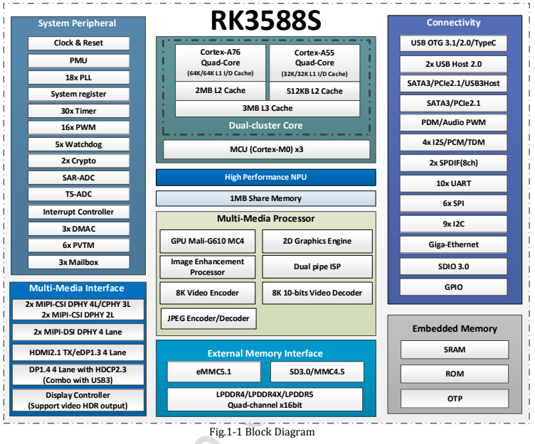
1-1. Block diagram (English original).
Additional diagram labels: 1MB shared memory; six PVTM blocks; two SPDIF blocks labelled “8ch”; system registers; embedded SRAM, ROM and OTP. The diagram labels the memory interface SD3.0/MMC4.5, while §1.2.2 specifies MMC4.51. These labels remain distinct.
2. Package information
2.1 Ordering
RK3588S and RK3588S-D are RoHS-compliant FCCSP1253L application processors, 900pcs by tray. The D part supports Dolby Audio; this distinction is not a compatibility guarantee for other variants.
2.2 Top marking
Rockchip identifies the brand; RKXXXX the chip; ABC the subcontractor; XXXXXX the die lot; DEFG the date code; NXXXXXX FXX the OSAT sub-lot. The dot identifies pin1. Photographs show YYWW in the date position, while the legend calls it DEFG.
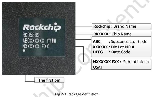
2-1. Package markings (English original).
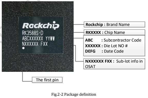
2-2. Package markings (English original).
2.3 Dimensions
Source figure2-4 is used twice, for bottom and side views; filenames distinguish them. Values are preserved in mm and inches.
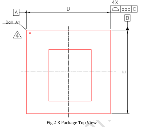
2-3. Package top view (English original).
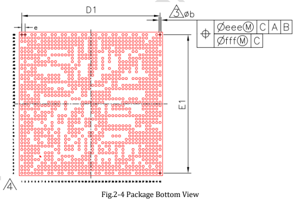
2-4-bottom. Package bottom view (English original).
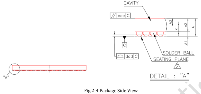
2-4-side. Package side view (English original).
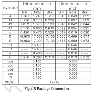
2-5. Package dimensions (English original).
| Symbol | mm Min | mm Nom | mm Max | inch Min | inch Nom | inch Max |
|---|---|---|---|---|---|---|
| A | 1.163 | 1.240 | 1.317 | 0.046 | 0.049 | 0.052 |
| A1 | 0.120 | 0.170 | 0.220 | 0.005 | 0.007 | 0.009 |
| A2 | 1.012 | 1.070 | 1.128 | 0.040 | 0.042 | 0.044 |
| A3 | 0.570 | 0.600 | 0.630 | 0.022 | 0.024 | 0.025 |
| c | 0.420 | 0.470 | 0.520 | 0.017 | 0.019 | 0.020 |
| D | 16.900 | 17.000 | 17.100 | 0.665 | 0.669 | 0.673 |
| E | 16.900 | 17.000 | 17.100 | 0.665 | 0.669 | 0.673 |
| D1 | — | 16.400 | — | — | 0.646 | — |
| E1 | — | 16.400 | — | — | 0.646 | — |
| e | — | 0.400 | — | — | 0.016 | — |
| b | 0.210 | 0.260 | 0.310 | 0.008 | 0.010 | 0.012 |
| aaa | 0.100 | 0.004 | ||||
| ccc | 0.150 | 0.006 | ||||
| ddd | 0.130 | 0.005 | ||||
| eee | 0.150 | 0.006 | ||||
| fff | 0.050 | 0.002 | ||||
| MD/ME | 42/42 |
2.4 Complete pin list
| Pin Name | Pin | Pin Name | Pin |
|---|---|---|---|
| VSS_1 | A1 | AVSS_98 | AY9 |
| VSS_2 | A2 | DDR_CH0_DQS0N_B | B1 |
| DDR_CH1_DQS1P_C | A3 | DDR_CH0_DQS0P_B | B2 |
| DDR_CH1_DQS1N_C | A4 | VSS_4 | B3 |
| DDR_CH1_ZQ_C | A5 | VSS_5 | B5 |
| DDR_CH1_WCK1N_C | A6 | DDR_CH1_WCK1P_C | B6 |
| DDR_CH1_A3_C | A7 | DDR_CH1_A6_C | B7 |
| DDR_CH1_DQS0P_C | A9 | VSS_6 | B8 |
| DDR_CH1_A4_C | A10 | DDR_CH1_DQS0N_C | B9 |
| DDR_CH1_DQ10_C | A12 | VSS_7 | B10 |
| DDR_CH1_LP4/4X_CKE1/LP5_CS1_C | A13 | VSS_8 | B11 |
| DDR_CH1_A5_C | A15 | DDR_CH1_DQ9_C | B12 |
| DDR_CH1_DQ14_C | A16 | DDR_CH1_RESET_C | B13 |
| DDR_CH1_LP4/4X_CKE0/LP5_CS0_C | A18 | VSS_9 | B14 |
| DDR_CH1_LP4/4X_CS1_C | A19 | DDR_CH1_LP4/4X_CS0_C | B15 |
| DDR_CH1_DQ2_C | A20 | DDR_CH1_DQ15_C | B16 |
| DDR_CH1_A1_C | A21 | VSS_10 | B17 |
| DDR_CH1_LP4/4X_CS1_D | A23 | DDR_CH1_A0_C | B18 |
| DDR_CH1_DQ0_D | A24 | VSS_11 | B19 |
| DDR_CH1_A0_D | A26 | DDR_CH1_DQ0_C | B20 |
| DDR_CH1_A1_D | A27 | VSS_12 | B21 |
| DDR_CH1_DQ3_D | A28 | DDR_CH1_A2_C | B22 |
| DDR_CH1_A2_D | A30 | VSS_13 | B23 |
| DDR_CH1_LP4/4X_CKE1/LP5_CS1_D | A31 | DDR_CH1_DQ2_D | B24 |
| DDR_CH1_DQ15_D | A32 | DDR_CH1_RESET_D | B25 |
| DDR_CH1_A6_D | A33 | VSS_14 | B26 |
| DDR_CH1_LP4/4X_CKE0/LP5_CS0_D | A35 | VSS_15 | B27 |
| DDR_CH1_A3_D | A36 | DDR_CH1_DQ5_D | B28 |
| DDR_CH1_WCK1P_D | A37 | VSS_16 | B29 |
| DDR_CH1_A5_D | A38 | DDR_CH1_LP4/4X_CS0_D | B30 |
| DDR_CH1_WCK0N_D | A39 | VSS_17 | B31 |
| DDR_CH1_ZQ_D | A40 | DDR_CH1_DQ12_D | B32 |
| DDR_CH1_DQS0N_D | A41 | DDR_CH1_A4_D | B33 |
| VSS_3 | A42 | VSS_18 | B34 |
| DDR_CH0_CKB_A | AA1 | VSS_19 | B35 |
| DDR_CH0_CK_A | AA2 | VSS_20 | B36 |
| VSS_296 | AA3 | DDR_CH1_WCK1N_D | B37 |
| DDR_CH0_DQ1_B | AA5 | VSS_21 | B38 |
| VSS_297 | AA6 | DDR_CH1_WCK0P_D | B39 |
| VSS_298 | AA7 | VSS_22 | B40 |
| VSS_299 | AA8 | DDR_CH1_DQS0P_D | B41 |
| VSS_300 | AA9 | VSS_23 | B42 |
| VSS_301 | AA10 | HDMI_TX0_SBDP/EDP_TX0_AUXP | BA1 |
| VSS_302 | AA11 | HDMI_TX0_D3P/EDP_TX0_D3P | BA2 |
| VSS_303 | AA12 | AVSS_116 | BA3 |
| DDR_CH0_PLL_AVSS | AA14 | HDMI_TX0_D0N/EDP_TX0_D0N | BA4 |
| VSS_304 | AA19 | HDMI_TX0_D1P/EDP_TX0_D1P | BA5 |
| VSS_305 | AA22 | AVSS_117 | BA6 |
| VSS_306 | AA23 | HDMI_TX0_D2N/EDP_TX0_D2N | BA7 |
| PLL_AVSS | AA26 | TYPEC0_SBU1/DP0_AUXP | BA8 |
| VDD_CPU_LIT_MEM_1 | AA28 | AVSS_118 | BA9 |
| VDD_CPU_LIT_MEM_2 | AA29 | TYPEC0_SSRX1N/DP0_TX0N | BA10 |
| VDD_CPU_LIT_MEM_3 | AA30 | TYPEC0_SSTX1N/DP0_TX1N | BA11 |
| VSS_307 | AA31 | AVSS_119 | BA12 |
| VSS_308 | AA37 | TYPEC0_SSRX2N/DP0_TX2N | BA13 |
| VSS_309 | AA38 | TYPEC0_SSTX2N/DP0_TX3N | BA14 |
| VSS_310 | AA39 | AVSS_120 | BA15 |
| VSS_311 | AA40 | MIPI_DPHY1_TX_D0N/MIPI_CPHY1_TX_TRIO0_A | BA16 |
| EMMC_D2/FSPI_D2_M0/GPIO2_D2_u | AA41 | MIPI_DPHY1_TX_D1P/MIPI_CPHY1_TX_TRIO1_A | BA17 |
| EMMC_D3/FSPI_D3_M0/GPIO2_D3_u | AA42 | AVSS_121 | BA18 |
| VSS_312 | AB2 | MIPI_DPHY1_TX_CLKN/MIPI_CPHY1_TX_TRIO1_B | BA19 |
| DDR_CH0_DQ3_A | AB3 | MIPI_DPHY1_TX_D2P/MIPI_CPHY1_TX_TRIO2_B | BA20 |
| DDR_CH0_DQ1_A | AB4 | AVSS_122 | BA21 |
| DDR_CH0_DQ4_A | AB5 | MIPI_DPHY1_TX_D3N/MIPI_CPHY1_TX_TRIO2_C | BA22 |
| VSS_313 | AB6 | MIPI_DPHY1_RX_D0P/MIPI_CPHY1_RX_TRIO0_B | BA23 |
| VSS_314 | AB9 | AVSS_123 | BA24 |
| VSS_315 | AB10 | MIPI_DPHY1_RX_D1N/MIPI_CPHY1_RX_TRIO0_C | BA25 |
| VSS_316 | AB11 | MIPI_DPHY1_RX_CLKP/MIPI_CPHY1_RX_TRIO1_C | BA26 |
| VSS_317 | AB12 | AVSS_124 | BA27 |
| DDR_CH0_PLL_DVDD | AB14 | MIPI_DPHY1_RX_D2N/MIPI_CPHY1_RX_TRIO2_A | BA28 |
| VSS_318 | AB19 | MIPI_DPHY1_RX_D3P/NO_USE | BA29 |
| VSS_319 | AB20 | AVSS_125 | BA30 |
| VSS_320 | AB21 | MIPI_DPHY0_TX_D0N/MIPI_CPHY0_TX_TRIO0_A | BA31 |
| VSS_321 | AB22 | MIPI_DPHY0_TX_D1P/MIPI_CPHY0_TX_TRIO1_A | BA32 |
| VSS_322 | AB23 | AVSS_126 | BA33 |
| VSS_323 | AB24 | MIPI_DPHY0_TX_CLKN/MIPI_CPHY0_TX_TRIO1_B | BA34 |
| PLL_AVDD1V8 | AB25 | MIPI_DPHY0_TX_D2P/MIPI_CPHY0_TX_TRIO2_B | BA35 |
| VDD_CPU_LIT_1 | AB31 | AVSS_127 | BA36 |
| VSS_324 | AB32 | MIPI_DPHY0_TX_D3N/MIPI_CPHY0_TX_TRIO2_C | BA37 |
| VSS_325 | AB33 | MIPI_DPHY0_RX_D0P/MIPI_CPHY0_RX_TRIO0_B | BA38 |
| VSS_326 | AB34 | MIPI_DPHY0_RX_D1P/MIPI_CPHY0_RX_TRIO1_A | BA40 |
| EMMCIO_1V8_1 | AB35 | MIPI_DPHY0_RX_CLKN/MIPI_CPHY0_RX_TRIO1_B | BA41 |
| VSS_327 | AB36 | MIPI_DPHY0_RX_D2N/MIPI_CPHY0_RX_TRIO2_A | BA42 |
| VSS_328 | AB37 | AVSS_128 | BB1 |
| VSS_329 | AB38 | HDMI_TX0_D3N/EDP_TX0_D3N | BB2 |
| VSS_330 | AB39 | HDMI_TX0_D0P/EDP_TX0_D0P | BB4 |
| VSS_331 | AB40 | HDMI_TX0_D1N/EDP_TX0_D1N | BB5 |
| EMMC_CLKOUT/GPIO2_A1_d | AB41 | HDMI_TX0_D2P/EDP_TX0_D2P | BB7 |
| EMMC_D4/I2C1_SCL_M3/UART5_RX_M2/GPIO2_D4_u | AB42 | TYPEC0_SBU2/DP0_AUXN | BB8 |
| DDR_CH0_LP4/4X_CS1_A | AC1 | TYPEC0_SSRX1P/DP0_TX0P | BB10 |
| DDR_CH0_A1_A | AC2 | TYPEC0_SSTX1P/DP0_TX1P | BB11 |
| VSS_332 | AC3 | TYPEC0_SSRX2P/DP0_TX2P | BB13 |
| VSS_333 | AC4 | TYPEC0_SSTX2P/DP0_TX3P | BB14 |
| VSS_334 | AC5 | MIPI_DPHY1_TX_D0P/MIPI_CPHY1_TX_TRIO0_B | BB16 |
| VSS_335 | AC6 | MIPI_DPHY1_TX_D1N/MIPI_CPHY1_TX_TRIO0_C | BB17 |
| VDD_VDENC_6 | AC16 | MIPI_DPHY1_TX_CLKP/MIPI_CPHY1_TX_TRIO1_C | BB19 |
| VSS_336 | AC17 | MIPI_DPHY1_TX_D2N/MIPI_CPHY1_TX_TRIO2_A | BB20 |
| VSS_337 | AC18 | MIPI_DPHY1_TX_D3P/NO_USE | BB22 |
| VSS_338 | AC22 | MIPI_DPHY1_RX_D0N/MIPI_CPHY1_RX_TRIO0_A | BB23 |
| VSS_339 | AC23 | MIPI_DPHY1_RX_D1P/MIPI_CPHY1_RX_TRIO1_A | BB25 |
| VSS_340 | AC24 | MIPI_DPHY1_RX_CLKN/MIPI_CPHY1_RX_TRIO1_B | BB26 |
| VSS_341 | AC25 | MIPI_DPHY1_RX_D2P/MIPI_CPHY1_RX_TRIO2_B | BB28 |
| VSS_342 | AC26 | MIPI_DPHY1_RX_D3N/MIPI_CPHY1_RX_TRIO2_C | BB29 |
| VDD_CPU_LIT_2 | AC27 | MIPI_DPHY0_TX_D0P/MIPI_CPHY0_TX_TRIO0_B | BB31 |
| VDD_CPU_LIT_3 | AC28 | MIPI_DPHY0_TX_D1N/MIPI_CPHY0_TX_TRIO0_C | BB32 |
| VDD_CPU_LIT_4 | AC29 | MIPI_DPHY0_TX_CLKP/MIPI_CPHY0_TX_TRIO1_C | BB34 |
| VDD_CPU_LIT_5 | AC30 | MIPI_DPHY0_TX_D2N/MIPI_CPHY0_TX_TRIO2_A | BB35 |
| VDD_CPU_LIT_6 | AC31 | MIPI_DPHY0_TX_D3P/NO_USE | BB37 |
| VCCIO5_1 | AC33 | MIPI_DPHY0_RX_D0N/MIPI_CPHY0_RX_TRIO0_A | BB38 |
| VCCIO5_2 | AC34 | MIPI_DPHY0_RX_CLKP/MIPI_CPHY0_RX_TRIO1_C | BB41 |
| EMMCIO_1V8_2 | AC35 | AVSS_129 | BB42 |
| SPI2_CS1_M2/I2C1_SCL_M1/UART0_RX_M1/GPIO0_B0_z | AC37 | DDR_CH0_ZQ_B | C1 |
| SDMMC_DET/GPIO0_A4_u | AC38 | VSS_24 | C2 |
| TSADC_SHUT_ORG/TSADC_SHUT/GPIO0_A1_z | AC39 | DDR_CH0_WCK0N_B | C3 |
| EMMC_DATA_STROBE/I2C2_SDA_M2/UART5_CTSN_M1/GPIO2_A2_d | AC40 | DDR_CH0_WCK0P_B | C4 |
| VSS_343 | AC41 | VSS_25 | C6 |
| DDR_CH0_LP4/4X_CKE1/LP5_CS1_A | AD1 | VSS_26 | C7 |
| VSS_344 | AD2 | DDR_CH1_WCK0P_C | C8 |
| VSS_345 | AD3 | VSS_27 | C9 |
| VSS_346 | AD5 | DDR_CH1_DQ11_C | C10 |
| VSS_347 | AD6 | VSS_28 | C11 |
| VSS_348 | AD8 | VSS_29 | C12 |
| VSS_349 | AD9 | DDR_CH1_DQ12_C | C13 |
| VSS_350 | AD10 | VSS_30 | C14 |
| VSS_351 | AD11 | VSS_31 | C15 |
| VSS_352 | AD12 | DDR_CH1_DQ5_C | C16 |
| VSS_353 | AD13 | DDR_CH1_DQ4_C | C17 |
| VSS_354 | AD14 | VSS_32 | C18 |
| VDD_VDENC_7 | AD15 | VSS_33 | C19 |
| VSS_355 | AD19 | VSS_34 | C20 |
| VSS_356 | AD20 | DDR_CH1_CK_C | C21 |
| VSS_357 | AD22 | VSS_35 | C22 |
| VSS_358 | AD23 | DDR_CH1_CK_D | C23 |
| VSS_359 | AD24 | VSS_36 | C24 |
| VSS_360 | AD25 | DDR_CH1_DQ1_D | C25 |
| VDD_CPU_LIT_7 | AD26 | VSS_37 | C26 |
| VDD_CPU_LIT_8 | AD27 | DDR_CH1_DQ6_D | C27 |
| CLK32K_IN/CLK32K_OUT0/GPIO0_B2_u | AD38 | VSS_38 | C28 |
| PMIC_SLEEP2/GPIO0_A3_d | AD39 | DDR_CH1_DQ7_D | C29 |
| EMMC_RSTN/I2C2_SCL_M2/UART5_RTSN_M1/GPIO2_A3_d | AD40 | VSS_39 | C30 |
| EMMC_D6/FSPI_CS0N_M0/GPIO2_D6_u | AD41 | DDR_CH1_DQ14_D | C32 |
| EMMC_D5/I2C1_SDA_M3/UART5_TX_M2/GPIO2_D5_u | AD42 | DDR_CH1_DM1_D | C33 |
| DDR_CH0_DM0_A | AE1 | DDR_CH1_DQ13_D | C34 |
| DDR_CH0_DQ6_A | AE2 | VSS_40 | C35 |
| DDR_CH0_DQ5_A | AE5 | DDR_CH1_DQS1N_D | C36 |
| VSS_361 | AE6 | VSS_41 | C37 |
| VSS_362 | AE7 | VSS_42 | C39 |
| VSS_363 | AE8 | AVSS_1 | C41 |
| VSS_364 | AE9 | PCIE20_2_RXN/SATA30_2_RXN/USB30_SSRXN | C42 |
| VSS_365 | AE10 | DDR_CH0_A3_B | D2 |
| VSS_366 | AE11 | VSS_43 | D3 |
| VSS_367 | AE12 | VSS_44 | D4 |
| VSS_368 | AE13 | VSS_45 | D7 |
| VSS_369 | AE14 | DDR_CH1_WCK0N_C | D8 |
| VSS_370 | AE15 | DDR_CH1_DQ8_C | D10 |
| VSS_371 | AE16 | VSS_46 | D11 |
| VSS_372 | AE19 | DDR_CH1_DM1_C | D13 |
| VSS_373 | AE20 | VSS_47 | D14 |
| VSS_374 | AE22 | VSS_48 | D15 |
| VSS_375 | AE23 | DDR_CH1_DQ7_C | D16 |
| VSS_376 | AE24 | DDR_CH1_DQ6_C | D17 |
| VSS_377 | AE25 | VSS_49 | D18 |
| VSS_378 | AE26 | VSS_50 | D19 |
| VDD_CPU_LIT_9 | AE27 | DDR_CH1_CKB_C | D21 |
| VSS_379 | AE38 | VSS_51 | D22 |
| VSS_380 | AE39 | DDR_CH1_CKB_D | D23 |
| VSS_381 | AE40 | DDR_CH1_DQ4_D | D25 |
| EMMC_D7/FSPI_CS1N_M0/GPIO2_D7_u | AE41 | VSS_52 | D26 |
| EMMC_CMD/FSPI_CLK_M0/GPIO2_A0_u | AE42 | DDR_CH1_DM0_D | D27 |
| DDR_CH0_A2_A | AF1 | DDR_CH1_DQ9_D | D29 |
| VSS_382 | AF2 | VSS_53 | D30 |
| DDR_CH0_DQ7_A | AF3 | VSS_54 | D31 |
| DDR_CH0_DQ14_A | AF4 | VSS_55 | D32 |
| DDR_CH0_DQ15_A | AF5 | DDR_CH1_DQ8_D | D34 |
| VSS_383 | AF6 | DDR_CH1_DQS1P_D | D36 |
| VSS_384 | AF7 | VOP_POST_EMPTY/I2C4_SDA_M3/UART6_RTSN_M1/PWM0_M2/SPI4_CLK_M2/GPIO1_A2_d | D38 |
| VSS_385 | AF8 | SPI2_CLK_M0/GPIO1_A6_d | D39 |
| VSS_386 | AF9 | UART7_TX_M2/SPI0_CS1_M2/GPIO1_B5_u | D40 |
| VSS_387 | AF10 | PCIE20_2_TXN/SATA30_2_TXN/USB30_SSTXN | D41 |
| VDD_LOGIC_5 | AF12 | PCIE20_2_RXP/SATA30_2_RXP/USB30_SSRXP | D42 |
| VDD_LOGIC_6 | AF13 | DDR_CH0_A4_B | E1 |
| VSS_388 | AF16 | VSS_56 | E2 |
| VSS_389 | AF17 | DDR_CH0_WCK1P_B | E3 |
| VSS_390 | AF19 | DDR_CH0_WCK1N_B | E4 |
| VSS_391 | AF20 | VSS_57 | E5 |
| VSS_392 | AF21 | VSS_58 | E6 |
| VSS_393 | AF26 | VSS_59 | E8 |
| VSS_394 | AF27 | VSS_60 | E9 |
| VSS_395 | AF28 | VSS_61 | E10 |
| VSS_396 | AF29 | VSS_62 | E12 |
| VSS_397 | AF30 | DDR_CH1_DQ13_C | E13 |
| VSS_398 | AF31 | VSS_63 | E16 |
| VSS_399 | AF32 | DDR_CH1_DM0_C | E17 |
| VSS_400 | AF33 | VSS_64 | E18 |
| VSS_401 | AF34 | VSS_65 | E19 |
| RESERVED | AF35 | DDR_CH1_DQ1_C | E20 |
| VCCIO5_1V8 | AF36 | VSS_66 | E21 |
| VSS_402 | AF37 | VSS_67 | E23 |
| VSS_403 | AF38 | VSS_68 | E25 |
| VSS_404 | AF39 | VSS_69 | E27 |
| VSS_405 | AF40 | DDR_CH1_DQ10_D | E29 |
| VSS_406 | AF41 | VSS_70 | E30 |
| DDR_CH0_RESET_A | AG1 | VSS_71 | E31 |
| DDR_CH0_A5_A | AG2 | DDR_CH1_DQ11_D | E32 |
| VSS_407 | AG3 | VSS_72 | E33 |
| VSS_408 | AG4 | VSS_73 | E34 |
| VSS_409 | AG5 | VSS_74 | E37 |
| VSS_410 | AG6 | VSS_75 | E38 |
| VSS_411 | AG7 | VSS_76 | E39 |
| VSS_412 | AG8 | AVSS_2 | E40 |
| VSS_413 | AG15 | PCIE20_2_TXP/SATA30_2_TXP/USB30_SSTXP | E41 |
| VSS_414 | AG16 | DDR_CH0_LP4/4X_CKE1/LP5_CS1_B | F1 |
| VSS_415 | AG17 | VSS_77 | F2 |
| VSS_416 | AG18 | VSS_78 | F3 |
| VSS_417 | AG19 | VSS_79 | F4 |
| VSS_418 | AG20 | VSS_80 | F8 |
| VSS_419 | AG21 | VSS_81 | F9 |
| VSS_420 | AG22 | VSS_82 | F10 |
| VSS_421 | AG23 | VSS_83 | F13 |
| VSS_422 | AG24 | VSS_84 | F14 |
| VSS_423 | AG25 | VSS_85 | F15 |
| VSS_424 | AG28 | VSS_86 | F16 |
| VSS_425 | AG29 | VSS_87 | F19 |
| VSS_426 | AG31 | DDR_CH1_DQ3_C | F20 |
| VSS_427 | AG32 | VSS_88 | F21 |
| VSS_428 | AG33 | VSS_89 | F23 |
| VSS_429 | AG34 | VSS_90 | F29 |
| VSS_430 | AG35 | VSS_91 | F31 |
| PMIC_SLEEP4/GPIO0_C2_d | AG36 | VSS_92 | F33 |
| LITCPU_AVS/SPI3_CLK_M2/GPIO0_D3_u | AG37 | VSS_93 | F34 |
| I2S1_SDI0_M1/GPU_AVS/UART0_TX_M0/I2C4_SCL_M2/PWM4_M0/GPIO0_C5_u | AG38 | VSS_94 | F35 |
| I2S1_SDI3_M1/PDM0_SDI1_M1/I2C6_SCL_M0/UART1_CTSN_M2/PWM7_IR_M0/SPI3_MISO_M2/GPIO0_D0_d | AG39 | VSS_95 | F36 |
| VSS_431 | AG40 | MIPI_CAMERA2_CLK_M0/SPDIF1_TX_M0/SATA2_ACT_LED_M1/I2C5_SDA_M3/UART1_RX_M1/PWM13_M2/GPIO1_B7_u | F37 |
| I2S1_SDO1_M1/I2C0_SDA_M2/UART1_RX_M2/SPI3_MOSI_M2/GPIO0_D2_u | AG41 | VSS_96 | F38 |
| PMIC_SLEEP6/PDM0_SDI3_M1/GPIO0_D6_d | AG42 | VSS_97 | F39 |
| VSS_432 | AH2 | AVSS_3 | F40 |
| VSS_433 | AH3 | PCIE20_2_REFCLKP | F41 |
| VSS_435 | AH5 | PCIE20_2_REFCLKN | F42 |
| VSS_436 | AH7 | DDR_CH0_DM1_B | G2 |
| VSS_437 | AH8 | VSS_98 | G3 |
| VSS_438 | AH9 | DDR_CH0_DQ10_B | G4 |
| VSS_439 | AH10 | DDR_CH0_DQ8_B | G5 |
| VDD_LOGIC_7 | AH11 | VSS_99 | G6 |
| VDD_LOGIC_8 | AH12 | VSS_100 | G8 |
| VDD_LOGIC_9 | AH13 | VSS_101 | G9 |
| VDD_LOGIC_10 | AH14 | VSS_102 | G10 |
| VDD_LOGIC_11 | AH15 | VSS_103 | G12 |
| VSS_440 | AH16 | VSS_104 | G20 |
| VSS_441 | AH17 | VSS_105 | G21 |
| VDD_GPU_1 | AH18 | VSS_106 | G22 |
| VDD_GPU_2 | AH19 | DDR_CH1_VDDQ_CKE | G24 |
| VDD_GPU_3 | AH20 | VSS_107 | G25 |
| VDD_GPU_4 | AH21 | VSS_108 | G26 |
| VDD_LOGIC_12 | AH23 | VCCIO4_1V8_1 | G27 |
| VDD_LOGIC_13 | AH24 | VCCIO4_1V8_2 | G28 |
| VDD_NPU_MEM_1 | AH25 | VSS_109 | G29 |
| VDD_NPU_MEM_2 | AH26 | VCCIO4 | G31 |
| VSS_442 | AH28 | PCIE20_SATA30_0_AVDD_1V8 | G34 |
| VSS_443 | AH29 | AVSS_4 | G36 |
| VSS_444 | AH36 | SPI2_MISO_M0/GPIO1_A4_d | G37 |
| TSADC_TEST_OUT_TS | AH37 | MIPI_CAMERA4_CLK_M0/I2C8_SDA_M2/UART1_CTSN_M1/PWM15_IR_M3/GPIO1_D7_u | G38 |
| PMIC_SLEEP5/GPIO0_C3_d | AH38 | PDM1_SDI2_M1/SPI0_MISO_M2/GPIO1_B1_d | G39 |
| I2S1_MCLK_M1/JTAG_TCK_M2/I2C1_SCL_M0/UART2_TX_M0/PCIE20X1_1_CLKREQN_M0/GPIO0_B5_d | AH39 | PCIE20X1_1_CLKREQN_M2/DP0_HPDIN_M2/I2C2_SDA_M4/UART6_RX_M1/SPI4_MISO_M2/GPIO1_A0_d | G40 |
| VSS_434 | AH4 | AVSS_5 | G41 |
| I2S1_SCLK_TX_M1/JTAG_TMS_M2/I2C1_SDA_M0/UART2_RX_M0/PCIE20X1_1_WAKEN_M0/GPIO0_B6_d | AH40 | DDR_CH0_A6_B | H1 |
| I2S1_SDO0_M1/CPU_BIG0_AVS/I2C0_SCL_M2/UART0_CTSN/UART1_TX_M2/SPI0_CS0_M0/HDMI_TX0_CEC_M1/GPIO0_D1_u | AH41 | DDR_CH0_LP4/4X_CKE0/LP5_CS0_B | H2 |
| I2S1_SDI1_M1/NPU_AVS/UART0_RTSN/PWM5_M1/SPI0_CLK_M0/SATA_CP_POD/GPIO0_C6_u | AH42 | VSS_110 | H3 |
| DDR_CH0_DQ2_A | AJ1 | VSS_111 | H4 |
| DDR_CH0_DQ0_A | AJ2 | VSS_112 | H5 |
| DDR_CH0_DQ12_A | AJ3 | VSS_113 | H6 |
| VSS_445 | AJ5 | VSS_114 | H11 |
| DDR_CH0_DQ11_A | AJ6 | VSS_115 | H12 |
| VSS_446 | AJ7 | DDR_CH1_VDDQ_1 | H14 |
| VSS_447 | AJ8 | DDR_CH1_VDDQ_2 | H15 |
| VSS_448 | AJ9 | DDR_CH1_VDDQ_3 | H16 |
| VSS_449 | AJ10 | DDR_CH1_VDDQ_4 | H18 |
| VSS_450 | AJ11 | DDR_CH1_VDDQ_5 | H20 |
| VSS_451 | AJ12 | VSS_116 | H22 |
| VDD_LOGIC_14 | AJ15 | DDR_CH1_VDDQ_CK | H24 |
| VSS_452 | AJ16 | VSS_117 | H25 |
| VDD_GPU_MEM_1 | AJ18 | VDD_LOGIC_1 | H27 |
| VDD_GPU_5 | AJ19 | VSS_118 | H29 |
| VDD_GPU_6 | AJ20 | VCCIO1_1V8 | H31 |
| VDD_GPU_7 | AJ21 | PCIE20_SATA30_USB30_2_AVDD_1V8 | H34 |
| VDD_NPU_MEM_3 | AJ25 | PCIE20_SATA30_0_AVDD_0V85 | H36 |
| VSS_453 | AJ26 | AVSS_6 | H37 |
| VSS_454 | AJ27 | PDM1_SDI0_M1/PCIE20X1_1_PERSTN_M2/PWM3_IR_M3/SPI2_CS0_M0/GPIO1_A7_u | H38 |
| VSS_455 | AJ28 | PDM1_SDI1_M1/SPI2_CS1_M0/GPIO1_B0_u | H39 |
| VSS_456 | AJ29 | AVSS_7 | H40 |
| VSS_457 | AJ30 | PCIE20_0_TXP/SATA30_0_TXP | H41 |
| VDD_LOGIC_15 | AJ31 | PCIE20_0_TXN/SATA30_0_TXN | H42 |
| VDD_LOGIC_16 | AJ32 | DDR_CH0_LP4/4X_CS0_B | J1 |
| VCCIO6_1V8 | AJ34 | VSS_119 | J2 |
| VSS_458 | AJ35 | DDR_CH0_DQ9_B | J3 |
| PMU_0V75_1 | AJ36 | DDR_CH0_DQ11_B | J4 |
| PMU_0V75_2 | AJ37 | DDR_CH0_DQ14_B | J5 |
| VSS_459 | AJ38 | VSS_120 | J6 |
| VSS_460 | AJ39 | VSS_121 | J7 |
| VSS_461 | AJ40 | VSS_122 | J8 |
| VSS_462 | AJ41 | VSS_123 | J9 |
| DDR_CH0_LP4/4X_CKE0/LP5_CS0_A | AK1 | VSS_124 | J10 |
| VSS_463 | AK2 | VSS_125 | J12 |
| DDR_CH0_DQ13_A | AK3 | VSS_126 | J14 |
| DDR_CH0_DM1_A | AK4 | VSS_127 | J15 |
| DDR_CH0_DQ8_A | AK5 | VSS_128 | J16 |
| VSS_464 | AK6 | DDR_CH1_VDD_1 | J18 |
| VSS_465 | AK7 | DDR_CH1_VDD_MIF_1 | J20 |
| NC | AK9 | VSS_129 | J22 |
| VCCIO2 | AK10 | VSS_130 | J24 |
| VCCIO2_1V8 | AK11 | VSS_131 | J26 |
| HDMI/eDP_TX0_VDD_IO_1V8 | AK12 | VDD_LOGIC_2 | J27 |
| VDD_LOGIC_17 | AK15 | VSS_132 | J29 |
| VSS_466 | AK16 | VSS_133 | J30 |
| VDD_GPU_MEM_2 | AK18 | VSS_134 | J31 |
| VDD_GPU_8 | AK21 | PCIE20_SATA30_USB30_2_AVDD_0V85 | J36 |
| VSS_467 | AK22 | AVSS_8 | J38 |
| VDD_NPU_MEM_4 | AK25 | AVSS_9 | J39 |
| VSS_468 | AK26 | AVSS_10 | J40 |
| VDD_NPU_1 | AK27 | PCIE20_0_RXN/SATA30_0_RXN | J41 |
| VDD_NPU_2 | AK28 | PCIE20_0_RXP/SATA30_0_RXP | J42 |
| VDD_NPU_3 | AK29 | DDR_CH0_DQS1P_B | K1 |
| VSS_469 | AK30 | DDR_CH0_DQS1N_B | K2 |
| I2S1_LRCK_TX_M1/PWM0_M0/I2C2_SCL_M0/SPI0_CS1_M0/PCIE20X1_1_PERSTN_M0/GPIO0_B7_d | AK39 | VSS_135 | K3 |
| VSS_470 | AK40 | VSS_136 | K6 |
| MIPI_CSI0_D1P | AK41 | VSS_137 | K7 |
| MIPI_CSI0_D1N | AK42 | DDR_CH0_VDDQ_CK_1 | K9 |
| DDR_CH0_A3_A | AL2 | VSS_138 | K10 |
| VSS_471 | AL3 | VSS_139 | K11 |
| VSS_472 | AL4 | VSS_140 | K12 |
| VSS_473 | AL5 | VSS_141 | K14 |
| HDMI/eDP_TX0_VDD_CMN_1V8 | AL14 | VSS_142 | K17 |
| AVSS_24 | AL15 | DDR_CH1_VDD_2 | K18 |
| VSS_474 | AL16 | DDR_CH1_VDD_MIF_2 | K20 |
| VDD_GPU_MEM_3 | AL18 | VSS_143 | K22 |
| VDD_GPU_9 | AL21 | VSS_144 | K23 |
| VSS_475 | AL22 | VSS_145 | K25 |
| VDD_NPU_4 | AL28 | VSS_146 | K26 |
| VDD_NPU_5 | AL29 | VDD_CPU_BIG0_MEM_1 | K27 |
| VDD_NPU_6 | AL30 | VDD_CPU_BIG0_MEM_2 | K28 |
| VDD_LOGIC_18 | AL31 | VDD_CPU_BIG0_MEM_3 | K29 |
| VCCIO6_1 | AL33 | VDD_CPU_BIG0_MEM_4 | K30 |
| VSS_476 | AL35 | VSS_147 | K31 |
| I2S1_LRCK_RX_M1/PDM0_CLK1_M1/PWM2_M0/UART0_RX_M0/I2C4_SDA_M2/DP0_HPDIN_M1/GPIO0_C4_d | AL38 | VSS_148 | K32 |
| I2S1_SDO2_M1/PDM0_SDI2_M1/PWM3_IR_M0/I2C1_SCL_M2/HDMI_TX0_SDA_M1/SPI3_CS0_M2/SATA_CPDET/GPIO0_D4_u | AL39 | VSS_149 | K33 |
| I2S1_SDI2_M1/PDM0_SDI0_M1/I2C6_SDA_M0/UART1_RTSN_M2/PWM6_M0/SPI0_MISO_M0/GPIO0_C7_d | AL40 | AVSS_11 | K34 |
| MIPI_CSI0_D0N | AL41 | AVSS_12 | K35 |
| MIPI_CSI0_D0P | AL42 | AVSS_13 | K36 |
| DDR_CH0_ZQ_A | AM1 | AVSS_14 | K37 |
| DDR_CH0_A6_A | AM2 | AVSS_15 | K38 |
| VSS_477 | AM4 | AVSS_16 | K39 |
| VSS_478 | AM5 | AVSS_17 | K40 |
| HDMI/eDP_TX0_VDD_0V75_1 | AM13 | PCIE20_0_REFCLKN | K41 |
| AVSS_25 | AM14 | DDR_CH0_A5_B | L1 |
| AVSS_26 | AM15 | VSS_150 | L2 |
| VSS_479 | AM16 | VSS_151 | L3 |
| VSS_480 | AM17 | VSS_152 | L5 |
| VDD_GPU_10 | AM21 | VSS_153 | L6 |
| VDD_GPU_11 | AM22 | DDR_CH0_VDDQ_CK_2 | L9 |
| VSS_481 | AM23 | VSS_154 | L10 |
| VSS_482 | AM25 | VSS_155 | L11 |
| VSS_483 | AM27 | VSS_156 | L12 |
| VDD_NPU_7 | AM30 | VSS_157 | L14 |
| VSS_484 | AM31 | DDR_CH1_PLL_AVDD1V8 | L15 |
| VSS_485 | AM32 | DDR_CH1_VDD_3 | L18 |
| VCCIO6_2 | AM33 | DDR_CH1_VDD_MIF_3 | L20 |
| MIPI_CSI0_AVCC1V8 | AM35 | VSS_158 | L22 |
| MIPI_CSI0_AVCC0V75 | AM37 | VSS_159 | L23 |
| PMIC_SLEEP3/GPIO0_C1_d | AM38 | VSS_160 | L24 |
| I2S1_SDO3_M1/CPU_BIG1_AVS/I2C1_SDA_M2/HDMI_TX0_SCL_M1/SPI3_CS1_M2/SATA_MP_SWITCH/GPIO0_D5_u | AM39 | VSS_161 | L32 |
| I2S1_SCLK_RX_M1/PDM0_CLK0_M1/PWM1_M0/I2C2_SDA_M0/SPI0_MOSI_M0/GPIO0_C0_d | AM40 | VSS_162 | L33 |
| VSS_486 | AM41 | AVSS_18 | L34 |
| DDR_CH0_DQS0P_A | AN1 | AVSS_19 | L35 |
| DDR_CH0_DQS0N_A | AN2 | VSS_163 | L36 |
| VSS_487 | AN3 | MIPI_CAMERA3_CLK_M0/I2C8_SCL_M2/UART1_RTSN_M1/PWM14_M2/GPIO1_D6_u | L37 |
| DDR_CH0_DQ10_A | AN4 | MIPI_CAMERA1_CLK_M0/SPDIF0_TX_M0/I2C5_SCL_M3/UART1_TX_M1/GPIO1_B6_u | L38 |
| DDR_CH0_DQ9_A | AN5 | I2C4_SCL_M3/UART6_CTSN_M1/PWM1_M2/SPI4_CS0_M2/GPIO1_A3_d | L39 |
| VSS_488 | AN6 | PCIE20X1_1_WAKEN_M2/I2C2_SCL_M4/UART6_TX_M1/SPI4_MOSI_M2/GPIO1_A1_d | L40 |
| VSS_489 | AN7 | AVSS_20 | L41 |
| OTP_VDDOTP_0V75 | AN8 | PCIE20_0_REFCLKP | L42 |
| HDMI/eDP_TX0_AVDD_0V75 | AN10 | DDR_CH0_LP4/4X_CS1_B | M1 |
| AVSS_27 | AN11 | VSS_164 | M2 |
| HDMI/eDP_TX0_VDD_0V75_2 | AN12 | VSS_165 | M5 |
| AVSS_28 | AN13 | DDR_CH0_VDDQ_CKE_1 | M6 |
| AVSS_29 | AN14 | DDR_CH0_VDDQ_CKE_2 | M7 |
| AVSS_30 | AN15 | VSS_166 | M8 |
| VSS_490 | AN17 | VSS_167 | M9 |
| AVSS_31 | AN18 | VSS_168 | M10 |
| VDD_GPU_12 | AN21 | VSS_169 | M12 |
| VDD_GPU_13 | AN22 | VSS_170 | M14 |
| VSS_491 | AN23 | DDR_CH1_PLL_DVDD | M16 |
| VSS_492 | AN25 | VSS_171 | M17 |
| VDD_NPU_8 | AN30 | VSS_172 | M19 |
| VSS_493 | AN31 | VSS_173 | M21 |
| VSS_494 | AN32 | VSS_174 | M22 |
| VSS_495 | AN33 | VSS_175 | M23 |
| VSS_496 | AN34 | VDD_CPU_BIG0_1 | M24 |
| VSS_497 | AN35 | VDD_CPU_BIG0_2 | M25 |
| VSS_498 | AN37 | VDD_CPU_BIG0_3 | M28 |
| VSS_499 | AN38 | VDD_CPU_BIG0_4 | M29 |
| VSS_500 | AN39 | VDD_CPU_BIG0_5 | M30 |
| VSS_501 | AN40 | AVSS_21 | M33 |
| MIPI_CSI0_CLK0N | AN41 | AVSS_22 | M34 |
| MIPI_CSI0_CLK0P | AN42 | VSS_176 | M35 |
| VSS_502 | AP2 | VSS_177 | M36 |
| VSS_503 | AP5 | PDM1_CLK1_M1/SATA0_ACT_LED_M1/UART4_TX_M2/SPI0_CLK_M2/GPIO1_B3_d | M37 |
| VSS_504 | AP6 | PDM1_SDI3_M1/UART4_RX_M2/SPI0_MOSI_M2/GPIO1_B2_d | M38 |
| AVSS_32 | AP7 | PDM1_CLK0_M1/UART7_RX_M2/SPI0_CS0_M2/GPIO1_B4_u | M39 |
| AVSS_33 | AP8 | HDMI_TX0_HPD_M0/SPI2_MOSI_M0/GPIO1_A5_d | M40 |
| AVSS_34 | AP9 | I2S0_LRCK_RX/PDM0_CLK0_M0/I2C4_SDA_M4/PWM15_IR_M2/GPIO1_C6_d | M41 |
| AVSS_35 | AP10 | I2S0_SCLK_TX/I2C6_SCL_M1/UART3_CTSN/PWM7_IR_M2/SPI4_CS0_M0/GPIO1_C3_d | M42 |
| AVSS_36 | AP11 | DDR_CH0_DQ2_B | N1 |
| AVSS_37 | AP16 | DDR_CH0_DQ13_B | N2 |
| TYPEC0_DP0_VDDA_0V85_1 | AP18 | VSS_178 | N3 |
| AVSS_38 | AP22 | DDR_CH0_DQ12_B | N5 |
| SARADC_AVDD_1V8 | AP23 | DDR_CH0_DQ15_B | N6 |
| VSS_505 | AP25 | VSS_179 | N7 |
| VSS_506 | AP27 | VSS_180 | N9 |
| VDD_NPU_9 | AP30 | VSS_181 | N11 |
| AVSS_39 | AP31 | VSS_182 | N12 |
| AVSS_40 | AP32 | DDR_CH1_PLL_AVSS | N15 |
| VSS_507 | AP33 | VSS_183 | N16 |
| VSS_508 | AP34 | VSS_184 | N17 |
| VSS_509 | AP35 | VSS_185 | N18 |
| VSS_510 | AP37 | VSS_186 | N21 |
| VSS_511 | AP38 | VSS_187 | N22 |
| VSS_512 | AP39 | VDD_CPU_BIG0_6 | N24 |
| VSS_513 | AP40 | VDD_CPU_BIG0_7 | N25 |
| MIPI_CSI0_D3N | AP41 | AVSS_23 | N33 |
| MIPI_CSI0_D3P | AP42 | VSS_188 | N34 |
| SDMMC_CLK/PDM1_CLK0_M0/TEST_CLKOUT_M0/MCU_JTAG_TMS_M0/UART5_TX_M0/GPIO4_D5_d | AR1 | OSC_1V8_1 | N35 |
| SDMMC_D1/PDM1_SDI2_M0/JTAG_TMS_M1/I2C3_SDA_M4/UART2_RX_M1/PWM9_M1/GPIO4_D1_u | AR2 | OSC_1V8_2 | N36 |
| VSS_514 | AR3 | PMUIO1_1V8_1 | N37 |
| VSS_515 | AR4 | VSS_189 | N38 |
| DDR_CH0_WCK0N_A | AR5 | VSS_190 | N39 |
| DDR_CH0_WCK0P_A | AR6 | VSS_191 | N40 |
| AVSS_41 | AR9 | I2C3_SCL_M0/UART3_TX_M0/SPI4_MOSI_M0/GPIO1_C1_z | N41 |
| AVSS_42 | AR16 | I2S0_SDI0/GPIO1_D4_d | N42 |
| AVSS_43 | AR18 | DDR_CH0_RESET_B | P1 |
| TYPEC0_DP0_VDDA_0V85_2 | AR19 | VSS_192 | P2 |
| AVSS_44 | AR20 | DDR_CH0_DQ5_B | P3 |
| AVSS_45 | AR21 | DDR_CH0_DQ4_B | P4 |
| AVSS_46 | AR22 | DDR_CH0_DQ7_B | P5 |
| TYPEC0_DP0_VDDH_1V8 | AR23 | VSS_193 | P6 |
| AVSS_47 | AR25 | VSS_194 | P7 |
| MIPI_D/C_PHY1_VDD | AR27 | VSS_195 | P8 |
| MIPI_D/C_PHY1_VDD_1V8_1 | AR30 | VSS_196 | P9 |
| MIPI_D/C_PHY0_VDD | AR33 | DDR_CH0_VDDQ_1 | P10 |
| MIPI_D/C_PHY1_VDD_1V2_1 | AR34 | VSS_197 | P12 |
| MIPI_D/C_PHY0_VDD_1V2_2 | AR35 | VDD_VDENC_1 | P15 |
| GMAC1_PPSTRIG/I2C3_SDA_M1/UART7_TX_M1/SPI1_MISO_M1/GPIO3_C0_d | AR36 | VSS_198 | P16 |
| GMAC1_TXD3/SDIO_D1_M1/I2S3_SCLK/AUDDSM_LN/FSPI_D2_M2/I2C6_SCL_M4/PWM11_IR_M0/SPI4_MOSI_M1/GPIO3_A1_u | AR37 | VSS_199 | P17 |
| GMAC1_TXD2/SDIO_D0_M1/I2S3_MCLK/FSPI_D0_M2/I2C6_SDA_M4/PWM10_M0/SPI4_MISO_M1/GPIO3_A0_u | AR38 | VSS_200 | P18 |
| GMAC1_RXD1/I2S2_SCLK_RX_M1/MIPI_CAMERA3_CLK_M1/PWM9_M0/GPIO3_B0_u | AR39 | VSS_201 | P19 |
| VSS_516 | AR40 | VDD_CPU_BIG0_8 | P23 |
| VSS_517 | AR41 | VSS_202 | P25 |
| SDMMC_D3/PDM1_SDI0_M0/JTAG_TMS_M0/I2C8_SDA_M0/UART5_RTSN_M0/PWM10_M1/GPIO4_D3_u | AT1 | VSS_203 | P26 |
| VSS_518 | AT2 | VSS_204 | P27 |
| DDR_CH0_WCK1N_A | AT3 | VSS_205 | P28 |
| DDR_CH0_WCK1P_A | AT4 | VSS_206 | P29 |
| VSS_519 | AT5 | VSS_207 | P30 |
| VSS_520 | AT6 | VSS_208 | P31 |
| AVSS_48 | AT7 | VSS_209 | P32 |
| AVSS_49 | AT8 | VSS_210 | P33 |
| USB20_AVDD_3V3 | AT10 | VSS_211 | P34 |
| USB20_DVDD_0V75_1 | AT11 | PDM0_SDI0_M0/SPI1_CS1_M2/GPIO1_D5_d | P38 |
| USB20_DVDD_0V75_2 | AT12 | I2S0_LRCK_TX/I2C2_SCL_M3/UART4_RTSN/GPIO1_C5_d | P39 |
| USB20_AVDD_1V8_1 | AT13 | I2S0_SDO3/I2S0_SDI2/PDM0_SDI2_M0/I2C1_SCL_M4/UART4_TX_M0/PWM0_M1/SPI1_CLK_M2/GPIO1_D2_d | P40 |
| USB20_AVDD_1V8_2 | AT14 | I2S0_SDO0/I2C4_SCL_M4/UART4_CTSN/GPIO1_C7_d | P41 |
| CIF_HREF/BT1120_D8/I2S1_SDO1_M0/PCIE20X1_1_BUTTON_RSTN/I2C7_SCL_M3/UART8_RTSN_M0/PWM14_M1/SPI0_CS0_M1/GPIO4_B2_u | AT15 | DDR_CH0_A2_B | R1 |
| AVSS_50 | AT16 | DDR_CH0_A1_B | R2 |
| TYPEC0_DP0_VDD_0V85 | AT18 | VSS_212 | R3 |
| AVSS_51 | AT19 | VSS_213 | R4 |
| AVSS_52 | AT20 | VSS_214 | R8 |
| AVSS_53 | AT21 | DDR_CH0_VDDQ_2 | R10 |
| AVSS_54 | AT22 | VDD_VDENC_2 | R15 |
| AVSS_55 | AT23 | VSS_215 | R16 |
| MIPI_D/C_PHY1_VREG | AT27 | VSS_216 | R20 |
| AVSS_56 | AT29 | VSS_217 | R21 |
| MIPI_D/C_PHY0_VDD_1V8_2 | AT30 | VDD_CPU_BIG0_9 | R23 |
| MIPI_D/C_PHY0_VREG | AT33 | VDD_CPU_BIG0_10 | R24 |
| VSS_521 | AT36 | VSS_218 | R25 |
| GMAC1_RXD0/MIPI_CAMERA2_CLK_M1/PWM8_M0/GPIO3_A7_u | AT37 | VDD_CPU_BIG1_1 | R26 |
| GMAC1_RXD2/SDIO_D2_M1/I2S3_LRCK/AUDDSM_LP/FSPI_D2_M2/UART8_TX_M1/SPI4_CLK_M1/GPIO3_A2_u | AT38 | VDD_CPU_BIG1_2 | R27 |
| GMAC1_TXCLK/SDIO_CMD_M1/I2S3_SDI/AUDDSM_RP/UART8_RTSN_M1/SPI4_CS1_M1/GPIO3_A4_d | AT39 | VDD_CPU_BIG1_3 | R28 |
| GMAC1_RXD3/SDIO_D3_M1/I2S3_SDO/AUDDSM_RN/FSPI_D3_M2/UART8_RX_M1/SPI4_CS0_M1/GPIO3_A3_u | AT40 | VDD_CPU_BIG1_4 | R29 |
| MIPI_CSI0_D2P | AT41 | VDD_CPU_BIG1_5 | R30 |
| MIPI_CSI0_D2N | AT42 | VDD_CPU_BIG1_6 | R31 |
| SDMMC_CMD/PDM1_CLK1_M0/MCU_JTAG_TCK_M0/UART5_RX_M0/PWM7_IR_M1/GPIO4_D4_u | AU1 | VDD_CPU_BIG1_7 | R32 |
| VSS_522 | AU2 | VDD_CPU_BIG1_8 | R33 |
| VSS_523 | AU3 | VSS_219 | R35 |
| VSS_524 | AU4 | PMUIO1_1V8_2 | R36 |
| USB20_HOST1_REXT | AU6 | I2C3_SDA_M0/UART3_RX_M0/SPI4_MISO_M0/GPIO1_C0_z | R38 |
| TYPEC0_USB20_OTG0_REXT | AU7 | I2S0_SDI1/PDM0_SDI3_M0/I2C1_SDA_M4/UART4_RX_M0/PWM1_M1/SPI1_CS0_M2/GPIO1_D3_d | R39 |
| AVSS_57 | AU8 | VSS_220 | T2 |
| CIF_D5/BT1120_D5/I2S1_SDI0_M0/I2C3_SDA_M2/UART3_TX_M2/SPI2_MOSI_M1/GPIO4_A5_d | AU15 | VSS_221 | T3 |
| AVSS_58 | AU16 | VSS_222 | T4 |
| AVSS_59 | AU18 | DDR_CH0_VDDQ_3 | T10 |
| AVSS_60 | AU19 | DDR_CH0_VDD_1 | T12 |
| AVSS_61 | AU21 | DDR_CH0_VDD_2 | T13 |
| MIPI_CAMERA0_CLK_M0/SPDIF1_TX_M1/I2S1_SDO0_M0/SATA2_ACT_LED_M0/I2C6_SCL_M3/UART8_RX_M0/SPI0_CS1_M1/GPIO4_B1_u | AU22 | VDD_VDENC_3 | T15 |
| BT1120_D11/UART9_RX_M1/PWM12_M1/SPI3_MISO_M1/GPIO4_B5_d | AU23 | VSS_224 | T16 |
| AVSS_62 | AU24 | VSS_225 | T17 |
| AVSS_63 | AU25 | VSS_226 | T18 |
| AVSS_64 | AU27 | VSS_227 | T20 |
| AVSS_65 | AU28 | VSS_228 | T21 |
| AVSS_66 | AU29 | VSS_229 | T24 |
| CIF_D11/PCIE20X1_2_CLKREQN_M0/HDMI_TX0_SCL_M2/I2C5_SCL_M0/SPI3_MOSI_M3/GPIO3_C7_u | AU30 | VSS_230 | T25 |
| AVSS_67 | AU31 | VDD_CPU_BIG1_9 | T26 |
| CIF_D8/FSPI_CS0N_M2/UART5_TX_M1/SPI3_CS0_M3/GPIO3_C4_u | AU34 | VSS_231 | T35 |
| VSS_525 | AU35 | VSS_232 | T36 |
| VSS_526 | AU38 | VSS_233 | T37 |
| VSS_527 | AU39 | VSS_234 | T38 |
| VSS_528 | AU40 | VSS_235 | T39 |
| MIPI_CSI0_CLK1P | AU41 | VSS_236 | T40 |
| MIPI_CSI0_CLK1N | AU42 | XIN_24M | T41 |
| SDMMC_D2/PDM1_SDI1_M0/JTAG_TCK_M0/I2C8_SCL_M0/UART5_CTSN_M0/GPIO4_D2_u | AV1 | XOUT_24M | T42 |
| SDMMC_D0/PDM1_SDI3_M0/JTAG_TCK_M1/I2C3_SCL_M4/UART2_TX_M1/PWM8_M1/GPIO4_D0_u | AV2 | VSS_223 | T7 |
| DDR_CH0_DQS1N_A | AV3 | DDR_CH0_A0_A | U1 |
| DDR_CH0_DQS1P_A | AV4 | DDR_CH0_A0_B | U2 |
| VSS_529 | AV5 | DDR_CH0_DQ0_B | U3 |
| USB20_HOST0_DM | AV6 | DDR_CH0_DQ6_B | U4 |
| USB20_HOST1_DP | AV7 | DDR_CH0_DQ3_B | U5 |
| AVSS_68 | AV8 | VSS_237 | U6 |
| AVSS_69 | AV9 | VSS_238 | U7 |
| TYPEC0_USB20_VBUSDET | AV10 | VSS_239 | U8 |
| SARADC_IN2 | AV11 | DDR_CH0_VDD_3 | U12 |
| AVSS_70 | AV12 | DDR_CH0_VDD_4 | U13 |
| SARADC_IN3 | AV13 | VDD_VDENC_4 | U15 |
| AVSS_71 | AV14 | VSS_240 | U16 |
| AVSS_72 | AV15 | VSS_241 | U17 |
| AVSS_73 | AV16 | VSS_242 | U18 |
| CIF_D6/BT1120_D6/I2S1_SDI1_M0/I2C5_SCL_M2/UART3_RX_M2/SPI2_CLK_M1/GPIO4_A6_d | AV18 | VSS_243 | U20 |
| CIF_D0/BT1120_D0/I2S1_MCLK_M0/PCIE20X1_1_CLKREQN_M1/UART9_RTSN_M1/SPI0_MISO_M1/GPIO4_A0_d | AV19 | VSS_244 | U21 |
| AVSS_74 | AV21 | VSS_245 | U22 |
| BT1120_D13/PCIE20X1_2_CLKREQN_M1/HDMI_TX0_SCL_M0/I2C5_SDA_M1/SPI3_CLK_M1/GPIO4_B7_u | AV22 | VSS_246 | U23 |
| CIF_VSYNC/BT1120_D9/I2S1_SDO2_M0/PCIE20X1_2_BUTTON_RSTN/I2C7_SDA_M3/UART8_CTSN_M0/PWM15_IR_M1/GPIO4_B3_u | AV23 | VSS_247 | U24 |
| AVSS_75 | AV25 | VSS_248 | U25 |
| CIF_D2/BT1120_D2/I2S1_LRCK_TX_M0/PCIE20X1_1_PERSTN_M1/SPI0_CLK_M1/GPIO4_A2_d | AV26 | VDD_CPU_BIG1_10 | U26 |
| CIF_CLKOUT/BT1120_D10/I2S1_SDO3_M0/DP0_HPDIN_M0/SPDIF0_TX_M1/UART9_TX_M1/PWM11_IR_M1/GPIO4_B4_u | AV27 | I2S0_SCLK_RX/PDM0_CLK1_M0/I2C2_SDA_M3/PWM11_IR_M2/SPI4_CS1_M0/GPIO1_C4_d | U35 |
| AVSS_76 | AV29 | I2S0_MCLK/I2C6_SDA_M1/UART3_RTSN/PWM3_IR_M2/SPI4_CLK_M0/GPIO1_C2_d | U36 |
| CIF_D10/SPI3_MISO_M3/GPIO3_C6_u | AV30 | I2S0_SDO1/I2C7_SCL_M0/UART6_TX_M2/SPI1_MISO_M2/GPIO1_D0_d | U37 |
| HDMI_TX0_HPD_M1/MCU_JTAG_TCK_M1/UART9_RX_M2/SPI0_CS0_M3/GPIO3_D4_d | AV31 | I2S0_SDO2/I2S0_SDI3/PDM0_SDI1_M0/I2C7_SDA_M0/UART6_RX_M2/SPI1_MOSI_M2/GPIO1_D1_d | U38 |
| AVSS_77 | AV32 | VSS_249 | U39 |
| AVSS_78 | AV33 | VSS_250 | U40 |
| CIF_D9/FSPI_CS1N_M2/UART5_RX_M1/SPI3_CS1_M3/GPIO3_C5_u | AV34 | VSS_251 | U41 |
| GMAC1_TXD1/I2S2_MCLK_M1/UART2_CTSN/GPIO3_B4_u | AV35 | DDR_CH0_CKB_B | V1 |
| VSS_530 | AV36 | DDR_CH0_CK_B | V2 |
| ETH1_REFCLKO_25M/MIPI_CAMERA1_CLK_M1/I2C4_SCL_M0/GPIO3_A6_d | AV37 | VSS_252 | V3 |
| GMAC1_RXCLK/SDIO_CLK_M1/MIPI_CAMERA0_CLK_M1/FSPI_CLK_M2/I2C4_SDA_M0/UART8_CTSN_M1/GPIO3_A5_d | AV38 | DDR_CH0_DM0_B | V5 |
| GMAC1_RXDV_CRS/I2S2_LRCK_RX_M1/MIPI_CAMERA4_CLK_M1/UART2_TX_M2/PWM2_M1/GPIO3_B1_d | AV39 | VSS_253 | V6 |
| GMAC1_MDC/MIPI_TE0/I2C8_SCL_M4/UART7_RTSN_M1/PWM14_M0/SPI1_CS0_M1/GPIO3_C2_d | AV40 | VSS_254 | V7 |
| VSS_531 | AV41 | VSS_255 | V8 |
| VSS_532 | AW3 | DDR_CH0_VDDQ_4 | V10 |
| VSS_533 | AW4 | DDR_CH0_VDD_MIF_1 | V12 |
| USB20_HOST0_REXT | AW5 | DDR_CH0_VDD_MIF_2 | V13 |
| USB20_HOST0_DP | AW6 | DDR_CH0_VDD_MIF_3 | V14 |
| USB20_HOST1_DM | AW7 | VSS_256 | V16 |
| AVSS_79 | AW8 | VSS_257 | V17 |
| AVSS_80 | AW9 | VSS_258 | V19 |
| TYPEC0_USB20_OTG_ID | AW10 | VSS_259 | V23 |
| TYPEC0_DP0_REXT | AW11 | VSS_260 | V24 |
| AVSS_81 | AW12 | VSS_261 | V25 |
| SARADC_IN5 | AW13 | VDD_CPU_BIG1_MEM_1 | V26 |
| AVSS_82 | AW14 | VDD_CPU_BIG1_MEM_2 | V27 |
| SARADC_IN0_BOOT | AW15 | VDD_CPU_BIG1_MEM_3 | V28 |
| AVSS_83 | AW16 | VDD_CPU_BIG1_MEM_4 | V29 |
| AVSS_84 | AW17 | VSS_262 | V30 |
| CIF_D1/BT1120_D1/I2S1_SCLK_TX_M0/PCIE20X1_1_WAKEN_M1/UART9_CTSN_M1/SPI0_MOSI_M1/GPIO4_A1_d | AW18 | VSS_263 | V31 |
| CIF_D4/BT1120_D4/I2S1_LRCK_RX_M0/I2C3_SCL_M2/UART0_RX_M2/SPI2_MISO_M1/GPIO4_A4_d | AW19 | VSS_264 | V32 |
| AVSS_85 | AW21 | VSS_265 | V33 |
| BT1120_D12/SATA0_ACT_LED_M0/I2C5_SCL_M1/PWM13_M1/SPI3_MOSI_M1/GPIO4_B6_d | AW22 | VSS_266 | V34 |
| BT1120_D14/PCIE20X1_2_WAKEN_M1/HDMI_TX0_SDA_M0/I2C8_SCL_M3/SPI3_CS0_M1/GPIO4_C0_u | AW23 | PMUIO2_1 | V35 |
| AVSS_86 | AW25 | PMUIO2_2 | V36 |
| CIF_D7/BT1120_D7/I2S1_SDI2_M0/I2C5_SDA_M2/SPI2_CS0_M1/GPIO4_A7_d | AW26 | PMUIO2_1V8_1 | V37 |
| CIF_CLKIN/BT1120_CLKOUT/I2S1_SDI3_M0/I2C6_SDA_M3/UART8_TX_M0/SPI2_CS1_M1/GPIO4_B0_d | AW27 | VSS_267 | V38 |
| AVSS_87 | AW28 | VSS_268 | V39 |
| AVSS_88 | AW29 | VSS_269 | V40 |
| MCU_JTAG_TMS_M1/UART9_TX_M2/PWM11_IR_M3/SPI0_CS1_M3/GPIO3_D5_d | AW30 | TVSS | V41 |
| CIF_D12/PCIE20X1_2_WAKEN_M0/HDMI_TX0_SDA_M2/I2C5_SDA_M0/UART4_RX_M1/PWM8_M2/SPI3_CLK_M3/GPIO3_D0_u | AW31 | NPOR | V42 |
| AVSS_89 | AW32 | VSS_270 | W2 |
| AVSS_90 | AW33 | VSS_271 | W5 |
| GMAC1_TXER/I2S2_SDI_M1/UART2_RX_M2/PWM3_IR_M1/GPIO3_B2_d | AW34 | VSS_272 | W7 |
| GMAC1_TXD0/I2S2_SDO_M1/UART2_RTSN/GPIO3_B3_u | AW35 | VSS_273 | W8 |
| AVSS_91 | AW36 | VSS_274 | W9 |
| GMAC1_MCLKINOUT/I2S2_LRCK_TX_M1/UART3_RX_M1/PWM13_M0/GPIO3_B6_d | AW37 | DDR_CH0_VDDQ_5 | W10 |
| GMAC1_PPSCLK/UART7_RX_M1/SPI1_CLK_M1/GPIO3_C1_d | AW38 | VDD_VDENC_5 | W16 |
| GMAC1_MDIO/MIPI_TE1/I2C8_SDA_M4/UART7_CTSN_M1/PWM15_IR_M0/SPI1_CS1_M1/GPIO3_C3_d | AW39 | VDD_VDENC_MEM_1 | W17 |
| AVSS_92 | AW40 | VSS_275 | W18 |
| MIPI_DPHY0_RX_D3P/NO_USE | AW41 | VSS_276 | W19 |
| MIPI_DPHY0_RX_D3N/MIPI_CPHY0_RX_TRIO2_C | AW42 | VSS_277 | W22 |
| HDMI_TX0_SBDN/EDP_TX0_AUXN | AY1 | VSS_278 | W23 |
| AVSS_93 | AY2 | VSS_279 | W24 |
| HDMI/eDP_TX0_REXT | AY3 | VSS_280 | W26 |
| AVSS_94 | AY4 | VDD_LOGIC_3 | W33 |
| AVSS_95 | AY5 | REFCLK_OUT/GPIO0_A0_d | W38 |
| AVSS_96 | AY7 | SPI2_MOSI_M2/I2C0_SDA_M0/GPIO0_A6_z | W39 |
| AVSS_97 | AY8 | SPI2_CS0_M2/I2C1_SDA_M1/PWM5_M0/UART0_TX_M1/GPIO0_B1_z | W40 |
| TYPEC0_USB20_OTG_DM | AY10 | PMIC_SLEEP1/GPIO0_A2_d | W41 |
| TYPEC0_USB20_OTG_DP | AY11 | PMIC_INT_L/GPIO0_A7_u | W42 |
| AVSS_99 | AY12 | DDR_CH0_A4_A | Y1 |
| SARADC_IN1 | AY13 | DDR_CH0_LP4/4X_CS0_A | Y2 |
| AVSS_100 | AY14 | VSS_281 | Y3 |
| SARADC_IN4 | AY15 | VSS_282 | Y4 |
| AVSS_101 | AY16 | VSS_283 | Y5 |
| AVSS_102 | AY17 | VSS_284 | Y6 |
| AVSS_103 | AY18 | DDR_CH0_VDDQ_6 | Y10 |
| CIF_D3/BT1120_D3/I2S1_SCLK_RX_M0/UART0_TX_M2/GPIO4_A3_d | AY19 | VSS_285 | Y11 |
| AVSS_104 | AY21 | DDR_CH0_PLL_AVDD1V8 | Y14 |
| AVSS_105 | AY22 | VDD_VDENC_MEM_2 | Y17 |
| AVSS_106 | AY23 | VSS_286 | Y18 |
| AVSS_107 | AY25 | VSS_287 | Y19 |
| BT1120_D15/SPDIF1_TX_M2/PCIE20X1_2_PERSTN_M1/HDMI_TX0_CEC_M0/I2C8_SDA_M3/PWM6_M1/SPI3_CS1_M1/GPIO4_C1_d | AY26 | VSS_288 | Y22 |
| CIF_D13/PCIE20X1_2_PERSTN_M0/UART4_TX_M1/PWM9_M2/SPI0_MISO_M3/GPIO3_D1_d | AY27 | VSS_289 | Y23 |
| AVSS_108 | AY28 | VSS_290 | Y24 |
| AVSS_109 | AY29 | PLL_DVDD0V75 | Y26 |
| CIF_D14/I2C7_SCL_M2/UART9_RTSN_M2/SPI0_MOSI_M3/GPIO3_D2_d | AY30 | VSS_291 | Y28 |
| CIF_D15/I2C7_SDA_M2/UART9_CTSN_M2/PWM10_M2/SPI0_CLK_M3/GPIO3_D3_d | AY31 | VSS_292 | Y29 |
| AVSS_110 | AY32 | VSS_293 | Y30 |
| AVSS_111 | AY33 | VSS_294 | Y31 |
| GMAC1_PTP_REF_CLK/I2C3_SCL_M1/SPI1_MOSI_M1/GPIO3_B7_d | AY34 | VSS_295 | Y32 |
| GMAC1_TXEN/I2S2_SCLK_TX_M1/UART3_TX_M1/PWM12_M0/GPIO3_B5_u | AY35 | VDD_LOGIC_4 | Y33 |
| AVSS_112 | AY36 | PMUIO2_1V8_2 | Y37 |
| AVSS_113 | AY37 | SPI2_MISO_M2/I2C0_SCL_M0/GPIO0_B3_z | Y38 |
| AVSS_114 | AY39 | SPI2_CLK_M2/SDMMC_PWREN/PMU_DEBUG/GPIO0_A5_d | Y39 |
| MIPI_DPHY0_RX_D1N/MIPI_CPHY0_RX_TRIO0_C | AY40 | EMMC_D1/FSPI_D1_M0/GPIO2_D1_u | Y40 |
| AVSS_115 | AY41 | EMMC_D0/FSPI_D0_M0/GPIO2_D0_u | Y41 |
| MIPI_DPHY0_RX_D2P/MIPI_CPHY0_RX_TRIO2_B | AY42 |
3. Electrical specifications
3.1 Absolute ratings
Exceeding these limits can permanently damage the device; prolonged exposure to absolute maxima impairs reliability.
| Parameters | Related Power Group | Min | Max | Unit |
|---|---|---|---|---|
| Supply voltage for CPU | VDD_CPU_BIG0 VDD_CPU_BIG1 VDD_CPU_LIT | -0.3 | 1.1 | V |
| Supply voltage for CPU memory | VDD_CPU_BIG0_MEM VDD_CPU_BIG1_MEM VDD_CPU_LIT_MEM | -0.3 | 1.1 | V |
| Supply voltage for GPU | VDD_GPU | -0.3 | 1.1 | V |
| Supply voltage for GPU memory | VDD_GPU_MEM | -0.3 | 1.1 | V |
| Supply voltage for NPU | VDD_NPU | -0.3 | 1.1 | V |
| Supply voltage for NPU memory | VDD_NPU_MEM | -0.3 | 1.1 | V |
| Supply voltage for VCODEC | VDD_VDENC | -0.3 | 0.95 | V |
| Supply voltage for VCODEC memory | VDD_VDENC_MEM | -0.3 | 0.95 | V |
| Supply voltage for core logic | VDD_LOGIC | -0.3 | 0.95 | V |
| 0.75V supply voltage | PMU_0V75 PLL_DVDD0V75 USB20_DVDD_0V75 HDMI/eDP_TX0_VDD_0V75 HDMI/eDP_TX0_AVDD_0V75 MIPI_CSI0_AVCC0V75 OTP_VDDOTP_0V75 | -0.3 | 0.95 | V |
| 0.85V supply voltage | DDR_CH0_VDD DDR_CH0_VDD_MIF DDR_CH0_PLL_DVDD DDR_CH1_VDD DDR_CH1_VDD_MIF DDR_CH1_PLL_DVDD TYPEC0_DP0_VDD_0V85 TYPEC0_DP0_VDDA_0V85 MIPI_D/C_PHY0_VDD MIPI_D/C_PHY1_VDD PCIE20_SATA30_0_AVDD_0V85 PCIE20_SATA30_USB30_2_AVDD_0V85 | -0.3 | 1.00 | V |
| 1.2V supply voltage | MIPI_D/C_PHY_VDD_1V2 | -0.3 | 1.35 | V |
| 1.8V supply voltage | DDR_CH0_PLL_AVDD1V8 DDR_CH1_PLL_AVDD1V8 PLL_AVDD1V8 USB20_AVDD_1V8 TYPEC0_DP0_VDDH_1V8 HDMI/eDP_TX0_VDD_CMN_1V8 HDMI/eDP_TX0_VDD_IO_1V8 MIPI_CSI0_AVCC1V8 MIPI_D/C_PHY_VDD_1V8 PCIE20_SATA30_0_AVDD_1V8 PCIE20_SATA30_USB30_2_AVDD_1V8 SARADC_AVDD_1V8 OSC_1V8 | -0.5 | 1.98 | V |
| 3.3V supply voltage | USB20_AVDD_3V3 | -0.5 | 3.63 | V |
| 1.8V only GPIO supply voltage | PMUIO1_1V8 EMMCIO_1V8 VCCIO1_1V8 | -0.5 | 1.98 | V |
| 1.8V/3.3V GPIO supply voltage | PMUIO2_1V8 VCCIO2_1V8 VCCIO4_1V8 VCCIO5_1V8 VCCIO6_1V8 | -0.5 | 3.63 | V |
| Supply voltage for DDR IO (LPDDR4/4X 0.6V; LPDDR5 0.5V) | DDR_CH0_VDDQ DDR_CH0_VDDQ_CK DDR_CH1_VDDQ DDR_CH1_VDDQ_CK | -0.3 | 0.7 | V |
| Supply voltage for DDR IO (LPDDR4/4X 1.1V; LPDDR5 1.05V) | DDR_CH0_VDDQ_CKE DDR_CH1_VDDQ_CKE | -0.3 | 1.25 | V |
| Storage Temperature | Tstg | -40 | 125 | ℃ |
| Max Conjunction Temperature | Tj | NA | 125 | ℃ |
3.2 Recommended operation
| Parameters | Symbol | Min | Typ | Max | Unit |
|---|---|---|---|---|---|
| Voltage for CPU BigCore 0 | VDD_CPU_BIG0 | 0.55 | 0.75 | 1.05 | V |
| Voltage for CPU BigCore 0 Memory | VDD_CPU_BIG0_MEM | 0.675 | 0.75 | 1.05 | V |
| Voltage for CPU BigCore 1 | VDD_CPU_BIG1 | 0.55 | 0.75 | 1.05 | V |
| Voltage for CPU BigCore 1 Memory | VDD_CPU_BIG1_MEM | 0.675 | 0.75 | 1.05 | V |
| Voltage for CPU LitCore and DSU | VDD_CPU_LIT | 0.55 | 0.75 | 0.95 | V |
| Voltage for CPU LitCore and DSU Memory | VDD_CPU_LIT_MEM | 0.675 | 0.75 | 0.95 | V |
| Voltage for GPU | VDD_GPU | 0.55 | 0.75 | 0.95 | V |
| Voltage for GPU Memory | VDD_GPU_MEM | 0.675 | 0.75 | 0.95 | V |
| Voltage for NPU | VDD_NPU | 0.55 | 0.75 | 0.95 | V |
| Voltage for NPU Memory | VDD_NPU_MEM | 0.675 | 0.75 | 0.95 | V |
| Voltage for VCODEC | VDD_VDENC | 0.675 | 0.75 | 0.825 | V |
| Voltage for VCODEC Memory | VDD_VDENC_MEM | 0.675 | 0.75 | 0.825 | V |
| Voltage for Logic | VDD_LOGIC | 0.675 | 0.75 | 0.825 | V |
| Voltage for PMU | PMU_0V75 | 0.675 | 0.75 | 0.825 | V |
| Digital GPIO Power (1.8V only) | PMUIO1_1V8, VCCIO1_1V8 | 1.65 | 1.8 | 1.95 | V |
| Digital GPIO Power (3.3V/1.8V) | PMUIO2_1V8, VCCIO2_1V8, VCCIO4_1V8, VCCIO5_1V8, VCCIO6_1V8 | 2.7 1.65 | 3.3 1.8 | 3.6 1.95 | V |
| eMMC IO Power (1.8V) | EMMCIO_1V8 | 1.65 | 1.8 | 1.95 | V |
| DDR CH0 Logic power(0.85V) | DDR_CH0_VDD, DDR_CH0_VDD_MIF, DDR_CH1_VDD, DDR_CH1_VDD_MIF | 0.675 | 0.85 | 0.935 | V |
| DDR CH0_PLL power(0.85V) | DDR_CH0_PLL_DVDD, DDR_CH1_PLL_DVDD | 0.675 | 0.75 | 0.8925 | V |
| DDR CH0_PLL power(1.8V) | DDR_CH0_PLL_AVDD1V8, DDR_CH1_PLL_AVDD1V8 | 1.62 | 1.8 | 1.98 | V |
| LPDDR4 IO VDDQ power | DDR_CH0_VDDQ, DDR_CH0_VDDQ_CK, DDR_CH1_VDDQ, DDR_CH1_VDDQ_CK | 0.57 | 0.6 | 0.63 | V |
| LPDDR4 Retention IO VDDQ Power | DDR_CH0_VDDQ_CKE, DDR_CH1_VDDQ_CKE | 1.045 | 1.1 | 1.155 | V |
| LPDDR5 IO VDDQ power | DDR_CH0_VDDQ, DDR_CH0_VDDQ_CK, DDR_CH1_VDDQ, DDR_CH1_VDDQ_CK | 0.475 | 0.5 | 0.525 | V |
| LPDDR5 Retention IO VDDQ Power | DDR_CH0_VDDQ_CKE, DDR_CH1_VDDQ_CKE | 1.0 | 1.05 | 1.1 | V |
| PLL Analog Power(0.75V) | PLL_DVDD0V75 | 0.675 | 0.75 | 0.8925 | V |
| PLL Analog Power(1.8V) | PLL_AVDD1V8 | 1.62 | 1.8 | 1.98 | V |
| USB 2.0 Analog Power (0.75V) | USB20_DVDD_0V75 | 0.6975 | 0.75 | 0.825 | V |
| USB 2.0 Analog Power (1.8V) | USB20_AVDD_1V8 | 1.674 | 1.8 | 1.98 | V |
| USB 2.0 Analog Power (3.3V) | USB20_AVDD_3V3 | 3.069 | 3.3 | 3.63 | V |
| USB & DP Analog Power (0.85V) | TYPEC0_DP0_VDD_0V85, TYPEC0_DP0_VDDA_0V85 | 0.8075 | 0.85 | 0.8925 | V |
| USB & DP Analog Power (1.8V) | TYPEC0_DP0_VDDH_1V8 | 1.71 | 1.8 | 1.89 | V |
| Combo PIPE PHY Analog Power(0.9V) | PCIE20_SATA30_0_AVDD_0V85, PCIE20_SATA30_USB30_2_AVDD_0V85 | 0.8 | 0.85 | 0.935 | V |
| Combo PIPE PHY Analog Power(1.8V) | PCIE20_SATA30_0_AVDD_1V8, PCIE20_SATA30_USB30_2_AVDD_1V8 | 1.62 | 1.8 | 1.98 | V |
| MIPI CSI DPHY Analog Power(0.75V) | MIPI_CSI0_AVCC0V75 | 0.675 | 0.75 | 0.825 | V |
| MIPI CSI DPHY Analog Power(1.8V) | MIPI_CSI0_AVCC1V8 | 1.62 | 1.8 | 1.98 | V |
| MIPI DCPHY Analog Power (0.85V) | MIPI_D/C_PHY_VDD, MIPI_D/C_PHY1_VDD | 0.7125 | 0.85 | 0.8925 | V |
| MIPI DCPHY Analog Power (1.2V) | MIPI_D/C_PHY_VDD_1V2 | 1.14 | 1.2 | 1.26 | V |
| MIPI DCPHY Analog Power (1.8V) | MIPI_D/C_PHY_VDD_1V8 | 1.71 | 1.8 | 1.89 | V |
| HDMI/eDP TX Digital Power (0.75V) | HDMI/eDP_TX0_VDD_0V75 | 0.675 | 0.75 | 0.85 | V |
| HDMI/eDP TX Analog Power (0.75V) | HDMI/eDP_TX0_AVDD_0V75 | 0.675 | 0.75 | 0.85 | V |
| HDMI/eDP TX Analog Power (1.8V) | HDMI/eDP_TX0_VDD_CMN_1V8 | 1.62 | 1.8 | 1.98 | V |
| HDMI/eDP TX Analog Power (1.8V) | HDMI/eDP_TX0_VDD_IO_1V8 | 1.62 | 1.8 | 1.98 | V |
| SARADC Analog Power(1.8V) | SARADC_AVDD_1V8 | 1.62 | 1.8 | 1.98 | V |
| OTP Analog Power(0.75V) | OTP_VDDOTP_0V75 | 0.675 | 0.75 | 0.825 | V |
| OSC Analog Power(1.8V) | OSC_1V8 | 1.65 | 1.8 | 1.95 | V |
| OSC input clock frequency | NA | 24 | NA | MHz | |
| Max CPU frequency | NA | NA | 2.2-2.4 | GHz | |
| Max GPU frequency | NA | NA | 1000 | MHz | |
| Max NPU frequency | NA | NA | 1000 | MHz | |
| Ambient Operating Temperature | TA | 0 | NA | 80 | ℃ |
3.3 DC characteristics
| Parameters | Symbol | Min | Typ | Max | Unit | |
|---|---|---|---|---|---|---|
| Digital 3.3V/1.8V GPIO @3.3V | Input Low Voltage | VIL | VSS | NA | 0.3*VDDO | V |
| Digital 3.3V/1.8V GPIO @3.3V | Input High Voltage | VIH | 0.7*VDDO | NA | VDDO | V |
| Digital 3.3V/1.8V GPIO @3.3V | Output Low Voltage | VOL | VSS | NA | 0.25*DVDD | V |
| Digital 3.3V/1.8V GPIO @3.3V | Output High Voltage | VOH | 0.75*DVDD | NA | DVDD | V |
| Digital 3.3V/1.8V GPIO @3.3V | Pullup Resistor | RRPU | 10 | NA | 100 | Kohm |
| Digital 3.3V/1.8V GPIO @3.3V | Pulldown Resistor | RRPD | 10 | NA | 100 | Kohm |
| Digital 3.3V/1.8V GPIO @1.8V | Input Low Voltage | VIL | VSS | NA | 0.3*VDDO | V |
| Digital 3.3V/1.8V GPIO @1.8V | Input High Voltage | VIH | 0.7*VDDO | NA | VDDO | V |
| Digital 3.3V/1.8V GPIO @1.8V | Output Low Voltage | VOL | VSS | NA | 0.25*DVDD | V |
| Digital 3.3V/1.8V GPIO @1.8V | Output High Voltage | VOH | 0.75*DVDD | NA | DVDD | V |
| Digital 3.3V/1.8V GPIO @1.8V | Pullup Resistor | RRPU | 10 | NA | 50 | Kohm |
| Digital 3.3V/1.8V GPIO @1.8V | Pulldown Resistor | RRPD | 10 | NA | 50 | Kohm |
| Digital 1.8V only GPIO @1.8V | Input Low Voltage | VIL | VSS | NA | 0.3*VDDO | V |
| Digital 1.8V only GPIO @1.8V | Input High Voltage | VIH | 0.7*VDDO | NA | VDDO | V |
| Digital 1.8V only GPIO @1.8V | Output Low Voltage | VOL | VSS | NA | 0.25*DVDD | V |
| Digital 1.8V only GPIO @1.8V | Output High Voltage | VOH | 0.75*DVDD | NA | DVDD | V |
| Digital 1.8V only GPIO @1.8V | Pullup Resistor | RRPU | 10 | NA | 50 | Kohm |
| Digital 1.8V only GPIO @1.8V | Pulldown Resistor | RRPD | 10 | NA | 50 | Kohm |
| eMMC IO @1.8V | Input Low Voltage | VIL | VSS | NA | 0.35*DVDD | V |
| eMMC IO @1.8V | Input High Voltage | VIH | 0.65*DVDD | NA | DVDD | V |
| eMMC IO @1.8V | Output Low Voltage | VOL | VSS | NA | 0.45 | V |
| eMMC IO @1.8V | Output High Voltage | VOH | DVDD-0.45 | NA | DVDD | V |
| eMMC IO @1.8V | Pullup Resistor | RRPU | 10 | NA | 50 | Kohm |
| eMMC IO @1.8V | Pulldown Resistor | RRPD | 10 | NA | 50 | Kohm |
| DDR IO | Input Low Voltage | VIL | NA | NA | Vref-0.14 | V |
| DDR IO | Input High Voltage | VIH | Vref+0.14 | NA | NA | V |
| DDR IO | Output Log Voltage | VOL | NA | NA | 0.2 | V |
| DDR IO | Output High Voltage | VOH | 0.25 | NA | NA | V |
| DDR IO | Input Low Current | IIL | -100/-500 | NA | 100/500 | Room/Hot uA |
| DDR IO | Input High Current | IIH | -100/-500 | NA | 100/500 | Room/Hot uA |
3.4 General IO
| Parameters | Symbol | Test condition | Min | Typ | Max | Unit | |
|---|---|---|---|---|---|---|---|
| Digital 3.3V/1.8V GPIO @3.3V | Input leakage current | IPAD | DVDD=Max, VPAD=0V or DVDD | -10 | NA | 10 | uA |
| Digital 3.3V/1.8V GPIO @3.3V | Input Hysteresis for Schmitt Trigger Operation | VH | 0.08* VDDO | NA | NA | V | |
| Digital 3.3V/1.8V GPIO @3.3V | Input pullup resistor current | IRPU | VPAD = 0V | -20 | NA | -180 | uA |
| Digital 3.3V/1.8V GPIO @3.3V | Input pulldown resistor current | IRPD | VPAD = VDDO | 20 | NA | 180 | uA |
| Digital 3.3V/1.8V GPIO @1.8V | Input leakage current | IPAD | DVDD=Max, VPAD=0V or DVDD | -10 | NA | 10 | uA |
| Digital 3.3V/1.8V GPIO @1.8V | Input Hysteresis for Schmitt Trigger Operation | VH | 0.1* VDDO | NA | NA | V | |
| Digital 3.3V/1.8V GPIO @1.8V | Input pullup resistor current | IRPU | VPAD = 0V | -20 | NA | -180 | uA |
| Digital 3.3V/1.8V GPIO @1.8V | Input pulldown resistor current | IRPD | VPAD = VDDO | 20 | NA | 180 | uA |
| Digital 1.8V only GPIO @1.8V | Input leakage current | IPAD | DVDD=Max, VPAD=0V or DVDD | -10 | NA | 10 | uA |
| Digital 1.8V only GPIO @1.8V | Input Hysteresis for Schmitt Trigger Operation | VH | 0.1* VDDO | NA | NA | V | |
| Digital 1.8V only GPIO @1.8V | Input pullup resistor current | IRPU | VPAD = 0V | -20 | NA | -170 | uA |
| Digital 1.8V only GPIO @1.8V | Input pulldown resistor current | IRPD | VPAD = VDDO | 20 | NA | 170 | uA |
| eMMC IO @1.8V | Input leakage current | IPAD | DVDD=Max, VPAD=0V or DVDD | -10 | NA | 10 | uA |
| eMMC IO @1.8V | Input Hysteresis for Schmitt Trigger Operation | VH | 0.1* DVDD | NA | NA | V | |
| eMMC IO @1.8V | Input pullup resistor current | IRPU | VPAD = 0V | -20 | NA | -170 | uA |
| eMMC IO @1.8V | Input pulldown resistor current | IRPD | VPAD = VDDO | 20 | NA | 170 | uA |
VDDO and DVDD both denote IO supply. Negative pull-up-current MIN/MAX entries retain source positions.
3.5.1 INT PLL
| Parameters | Symbol | Test condition | Min | Typ | Max | Unit |
|---|---|---|---|---|---|---|
| Input clock frequency | FFIN | 4.5 | - | 300 | MHz | |
| Reference frequency(FFIN/p) | FFREE | 4.5 | 7 | 12 | MHz | |
| Frequency of PLL’s output | FFOUT | 35.2 | - | 4500 | MHz | |
| Frequency of VCO’s output | FFVCO | 2250 | - | 4500 | MHz | |
| Lock time | TLT | Measured at all FFIN and FFOUT range. RESETB=High | - | - | 150 | Cycles |
3.5.2 FRAC PLL
| Parameters | Symbol | Test condition | Min | Typ | Max | Unit |
|---|---|---|---|---|---|---|
| Input clock frequency | FFIN | 6 | - | 300 | MHz | |
| Reference frequency(FFIN/p) | FFREE | 6 | 20 | 30 | MHz | |
| Frequency of PLL’s output | FFOUT | 35.2 | - | 4500 | MHz | |
| Frequency of VCO’s output | FFVCO | 2250 | - | 4500 | MHz | |
| Lock time | TLT | Measured at all FFIN and FFOUT range. RESETB=High | - | - | 500 | Cycles |
3.5.3 DDR PLL
| Parameters | Symbol | Test condition | Min | Typ | Max | Unit |
|---|---|---|---|---|---|---|
| Input clock frequency | FFIN | 6 | - | 300 | MHz | |
| Reference frequency(FFIN/p) | FFREE | 6 | 20 | 30 | MHz | |
| Frequency of PLL’s output | FFOUT | 51.6 | - | 6600 | MHz | |
| Frequency of VCO’s output | FFVCO | 3300 | - | 6600 | MHz | |
| Lock time | TLT | Measured at all FFIN and FFOUT range. RESETB=High | - | - | 500 | Cycles |
Note①: p is the input-divider value.
3.6 PCIe2/SATA
| Parameters | Symbol | Min | Typ | Max | Unit |
|---|---|---|---|---|---|
| Transmitter | |||||
| Differential Peak-Peak TX Output Voltage Swing | VTX_DIFF_PP | 800 | 1000 | 1200 | mV |
| Differential Peak-Peak Low Power TX Output Voltage Swing | VTX_DIFF_PP_LOW | 400 | NA | 1200 | mV |
| The output impedance | RTX_DIFF_DC | 80 | 100 | 120 | ohm |
| Single Ended Output Resistance Matching | RTX_DC_OFFSET | NA | NA | 5 | % |
| Transmitter output common mode voltage | VTX_DC_CM | 400 | NA | 800 | mV |
| Maximum mismatch between TXP and TXM for both time and amp | VTX_CM_AC_PP_ACTIVE | NA | NA | 50 | mV |
| The amount of voltage change allowed during Receiver Detection | VTX_RCV_DETECT | NA | NA | 600 | mV |
| TX de-emphasis | VTX_DE_RATIO | 3.0 | 3.5 | 4.0 | dB |
| AC Coupling Capacitor(USB3.1/PCIe) | CAC_COUPLING | 75 | NA | 200 | nF |
| AC Coupling Capacitor(SATA) | CAC_COUPLING | 6 | NA | 12 | nF |
| Output rising time for 20% to 80% | Tr | 25 | NA | NA | ps |
| Output falling time for 20% to 80% | Tf | 25 | NA | NA | ps |
| Transmitter short circuit limit | ITX_SHORT | NA | NA | 20 | mA |
| Output differential skew | TSKEW_DIFF | -15 | NA | 15 | ps |
| Receiver | |||||
| Input Voltage Swing | VRXDPP_C | 250 | NA | 1200 | mVpp |
| The input differential impedance | RRXD_C | 80 | 100 | 120 | Ohm |
| Single Ended input Resistance Matching | RRXD_C_MS | NA | NA | 5 | % |
3.7 MIPI CDPHY
| Parameters | Symbol | Description | Test condition | Min | Typ | Max | Unit |
|---|---|---|---|---|---|---|---|
| LP-RX | VIH | Logic1 input voltage | All conditions | 880 | NA | NA | mV |
| LP-RX | VIL | Logic0 input voltage, not in ULPS state | All conditions | NA | NA | 550 | mV |
| Skew Calibration | Tskewcal (initial) | Duration for which the transmitter drives the skew-calibration pattern in the initial skew calibration mode | >1.5Gbps | NA | NA | 100 | us |
| Skew Calibration | Tskewcal (initial) | Duration for which the transmitter drives the skew-calibration pattern in the initial skew calibration mode | >1.5Gbps | 2^15 | NA | NA | UI |
| Skew Calibration | Tskewcal (periodic) | Duration for which the transmitter drives the skew-calibration pattern in the periodic skew calibration mode | >1.5Gbps (optional) | NA | NA | 10 | us |
| Skew Calibration | Tskewcal (periodic) | Duration for which the transmitter drives the skew-calibration pattern in the periodic skew calibration mode | >1.5Gbps (optional) | 2^13 | NA | NA | UI |
3.8 MIPI CSI DPHY
| Parameters | Symbol | Min | Typ | Max | Units |
|---|---|---|---|---|---|
| Common-mode interference beyond 450 MHz | ΔVCMRX(HF) | NA | NA | 100 | mV |
| Common-mode interference beyond 450 MHz | ΔVCMRX(HF) | NA | NA | 50 | mV |
| Common-mode interference 50MHz- 450MHz | ΔVCMRX(LF) | -50 | NA | 50 | mV |
| Common-mode interference 50MHz- 450MHz | ΔVCMRX(LF) | -25 | NA | 25 | mV |
| Common-mode termination | CCM | NA | NA | 60 | pF |
| Input pulse rejection | eSPIKE | NA | NA | 300 | V.ps |
| Minimum pulse width response | TMIN-RX | 20 | NA | NA | ns |
| Peak interference amplitude | VINT | NA | NA | 200 | mV |
| Interference frequency | fINT | 450 | NA | NA | MHz |
3.9 SARADC
| Parameters | Symbol | Test condition | Min | Typ | Max | Unit |
|---|---|---|---|---|---|---|
| Resolution | NA | 12 | NA | Bit | ||
| Anglog Input Range | AIN | AVSS18 | NA | AVDD18 | V | |
| Differential Non-Linearity | DNL | PD = Low Fs = 1MS/s FCLK = 20MHz FSOC = 1MHz FAIN = 10kHz ramp wave | NA | ±1.0 | ±3.0 | LSB |
| Integral Non-Linearity | INL | PD = Low Fs = 1MS/s FCLK = 20MHz FSOC = 1MHz FAIN = 10kHz ramp wave | NA | ±2.0 | ±6.0 | LSB |
| Top Offset Voltage Error | EOT | PD = Low Fs = 1MS/s FCLK = 20MHz FSOC = 1MHz FAIN = 10kHz ramp wave | NA | ±10 | ±20 | LSB |
| Bottom Offset Voltage Error | EOB | PD = Low Fs = 1MS/s FCLK = 20MHz FSOC = 1MHz FAIN = 10kHz ramp wave | NA | ±10 | ±20 | LSB |
3.10 TSADC
| Parameters | Symbol | Test condition | Min | Typ | Max | Unit |
|---|---|---|---|---|---|---|
| Accuracy from -40℃ to 125℃ | TJACC | Temp: -40 ~ 125℃ Supply: 1.62V ~ 1.98V | NA | ±3 | ±5 | ℃ |
| Sensing Temperature Range | TRANGE | -40 | 25 | 125 | ℃ | |
| Resolution | TLSB | NA | 1 | NA | ℃ |
4. Thermal management
For reliability and operation, the absolute maximum junction temperature must remain below 125°C. The package thermal values are simulation references and must be checked against physical testing. The reference PCB has 10 layers, dimensions 200mm x 130mm, at 25°C ambient.
| Parameter | Symbol | Typical | Unit |
|---|---|---|---|
| Junction-to-ambient thermal resistance | 𝜽 𝑱𝑨 | 8.2 | (℃/𝑾) |
| Junction-to-board thermal resistance | 𝜽 𝑱𝑩 | 3.7 | (℃/𝑾) |
| Junction-to-case thermal resistance | 𝜽 𝑱𝑪 | 0.01 | (℃/𝑾) |
Source qualifications
Features depend on the actual product configuration; some may require third-party licenses. This source does not list LPDDR5X or the later display/VOP timing requirements. The block diagram says Mali-G610 MC4, while feature text describes four shader cores; the source label is preserved, not silently changed to another variant. No moisture-level or ball-material subsection is present in this version.
Source qualifications
The block diagram labels six SPI blocks; §1.2.13 specifies five SPI controllers SPI0–SPI4. The source gives two HF common-mode-interference maxima and two LF ranges without conditions; all rows remain. Absolute maximum junction temperature is 125°C in the table, while thermal prose requires below125°C. This datasheet provides no register-map chapter.