
Chinese source V1.0.0, kernel scope 4.4 / 4.19. The technical preface introduces RK809 submodule concepts, functions, DTS configuration and troubleshooting; the full technical body is retained. No English PDF is available. All four languages use Chinese-PDF original figures, some already bearing English labels. Platform reference only: verify the actual ArmSoM PMIC, SoC, power tree, pins, SDK/BSP and kernel. Not a claim of support on every ArmSoM board; no hardware testing was performed.
Voltage, pin-mode and register writes can power off or damage hardware; these are unexecuted source examples. Source
0.737.5, differences between voltage/sequence tables,regulator-ramp-delay12500 versus example 6001, and the claimed four functions versus actual list count are retained without guessing corrections. Verify the source shutdown location “PCIE”, rockchi path and DCDC3 external-divider-only claim versus internal voltage settings in the sequence table against the BSP. Source headings 3.1/3.2 only say “kernel”; no version was invented.
1. Basics
1.1 Overview
RK809 is a high-performance PMIC integrating 5 high-current DCDCs, 9 LDOs, 2 SWITCH outputs, 1 RTC, 1 high-performance CODEC and adjustable power-up sequencing. System supplies are divided into DCDC and LDO types, with the following general characteristics; consult further references for details.
-
DCDC: efficient at a large input/output voltage difference, but with relatively high ripple and cost; therefore used for large voltage drops and high-current loads. Two common modes are PWM, with good ripple/transient response but lower efficiency, and PFM, with higher efficiency but weaker load capability.
-
LDO: low efficiency at a large input/output voltage difference, but low cost. Optimize the system to improve conversion efficiency: for a 1.1V LDO output, its input can be supplied by the VCCIO_3.3V DCDC. Where the circuit permits, connect the LDO input to a DCDC output, taking power-up sequencing into account.
1.2 Functions
From the user perspective, RK809 functions are described as four parts:
-
regulator: controls the state of individual DCDC and LDO supplies.
-
rtc: provides clockkeeping, timing and related functions.
-
gpio: ordinary GPIO operation with pinctrl functionality.
-
pwrkey: detects power-key press/release, saving one AP GPIO.
-
clk: two 32.768KHZ clock outputs; one is always on and cannot be controlled, while the other is software-controlled.
-
codec: sampling up to 192KHZ, 16bit and 32bit, DAC, ADC, PDM and other functions. Not covered here; the source states that a dedicated document will explain it later.
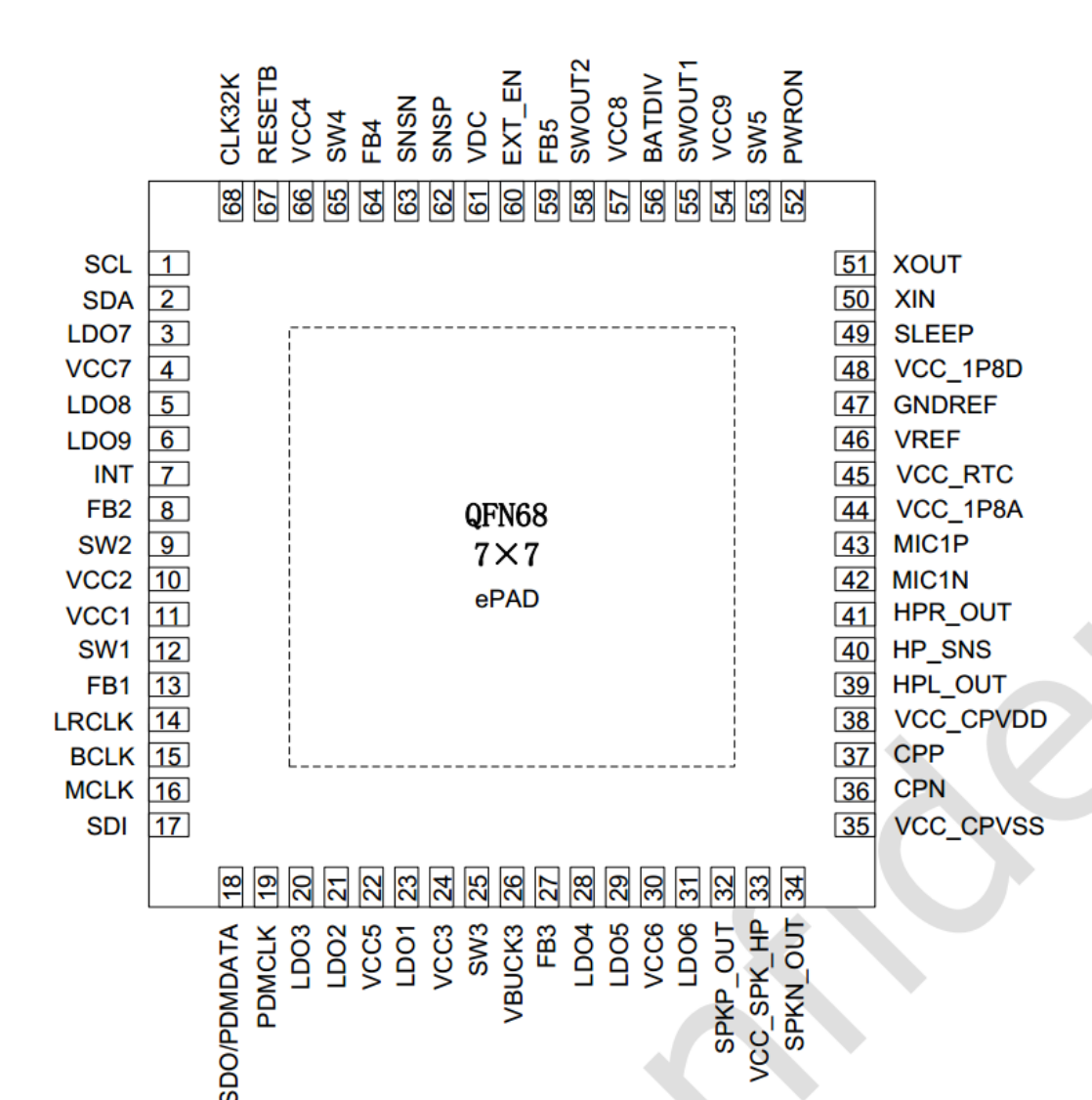
1.3 Pin functions
Chinese PDF original · p6
Pay particular attention to SLEEP and INT; the sleep pin also provides extended GPIO functionality.
Chinese PDF original · p7
Chinese PDF original · p7
Chinese PDF original · p8
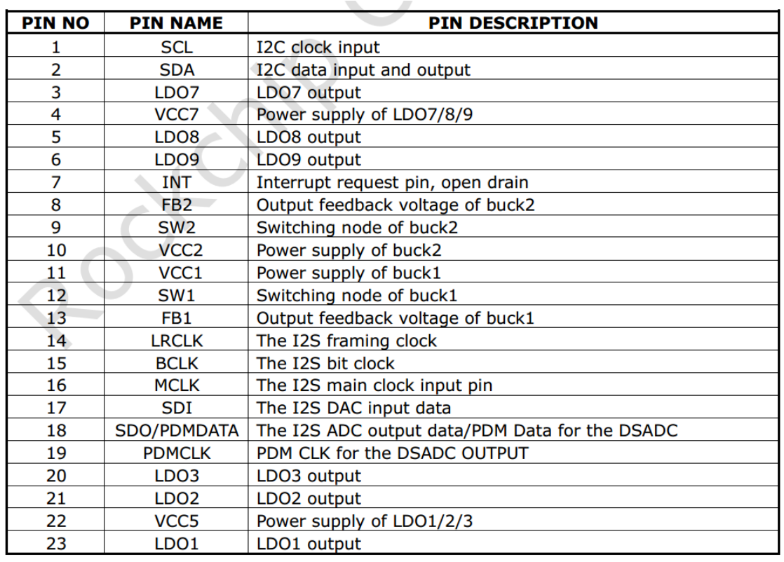
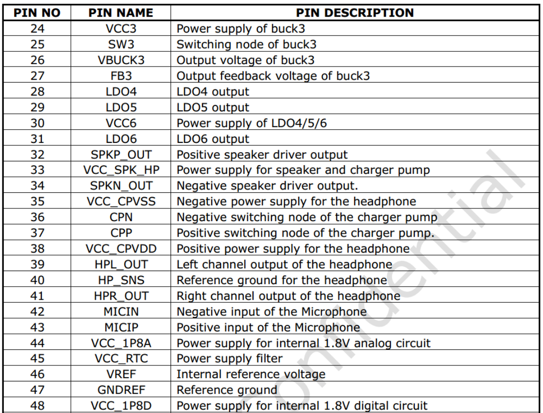
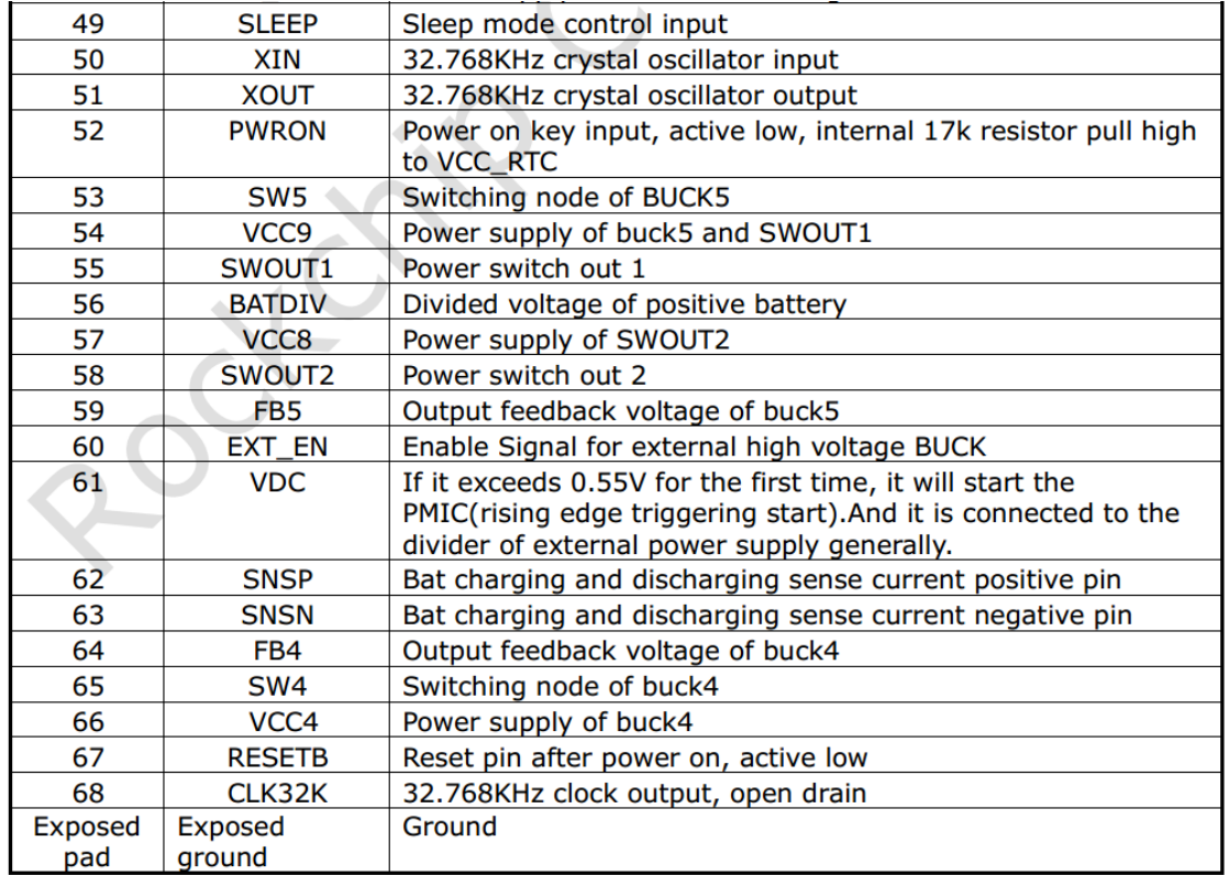
Editable transcription of the original tables above.
| Pin no. | Name | Description |
|---|---|---|
| 1 | SCL | I2C clock input |
| 2 | SDA | I2C data input/output |
| 3 | LDO7 | LDO7 output |
| 4 | VCC7 | Power supply of LDO7/8/9 |
| 5 | LDO8 | LDO8 output |
| 6 | LDO9 | LDO9 output |
| 7 | INT | Interrupt request, open drain |
| 8 | FB2 | Output feedback voltage of BUCK2 |
| 9 | SW2 | Switching node of BUCK2 |
| 10 | VCC2 | Power supply of BUCK2 |
| 11 | VCC1 | Power supply of BUCK1 |
| 12 | SW1 | Switching node of BUCK1 |
| 13 | FB1 | Output feedback voltage of BUCK1 |
| 14 | LRCLK | I2S framing clock |
| 15 | BCLK | I2S bit clock |
| 16 | MCLK | I2S main-clock input |
| 17 | SDI | I2S DAC input data |
| 18 | SDO/PDMDATA | I2S ADC output data/PDM data for DSADC |
| 19 | PDMCLK | PDM CLK for DSADC output |
| 20 | LDO3 | LDO3 output |
| 21 | LDO2 | LDO2 output |
| 22 | VCC5 | Power supply of LDO1/2/3 |
| 23 | LDO1 | LDO1 output |
| 24 | VCC3 | Power supply of BUCK3 |
| 25 | SW3 | Switching node of BUCK3 |
| 26 | VBUCK3 | BUCK3 output |
| 27 | FB3 | Output feedback voltage of BUCK3 |
| 28 | LDO4 | LDO4 output |
| 29 | LDO5 | LDO5 output |
| 30 | VCC6 | Power supply of LDO4/5/6 |
| 31 | LDO6 | LDO6 output |
| 32 | SPKP_OUT | Positive speaker-driver output |
| 33 | VCC_SPK_HP | Power supply for speaker and charge pump |
| 34 | SPKN_OUT | Negative speaker-driver output |
| 35 | VCC_CPVSS | Negative headphone power supply |
| 36 | CPN | Negative charge-pump switching node |
| 37 | CPP | Positive charge-pump switching node |
| 38 | VCC_CPVDD | Positive headphone power supply |
| 39 | HPL_OUT | Left headphone-channel output |
| 40 | HP_SNS | Headphone reference ground |
| 41 | HPR_OUT | Right headphone-channel output |
| 42 | MICIN | Negative microphone input |
| 43 | MICIP | Positive microphone input |
| 44 | VCC_1P8A | Supply for internal 1.8V analog circuit |
| 45 | VCC_RTC | Power-supply filter |
| 46 | VREF | Internal reference voltage |
| 47 | GNDREF | Reference ground |
| 48 | VCC_1P8D | Supply for internal 1.8V digital circuit |
| 49 | SLEEP | Sleep-mode control input |
| 50 | XIN | 32.768KHz crystal oscillator input |
| 51 | XOUT | 32.768KHz crystal oscillator output |
| 52 | PWRON | Power-key input, active low, internal 17k pull-up to VCC_RTC |
| 53 | SW5 | Switching node of BUCK5 |
| 54 | VCC9 | Power supply of BUCK5 / SWOUT1 |
| 55 | SWOUT1 | SWITCH1 output |
| 56 | BATDIV | Divided positive-battery voltage |
| 57 | VCC8 | Power supply of SWOUT2 |
| 58 | SWOUT2 | SWITCH2 output |
| 59 | FB5 | Output feedback voltage of BUCK5 |
| 60 | EXT_EN | Enable for external high-voltage BUCK |
| 61 | VDC | First crossing above 0.55V starts the PMIC (rising-edge trigger); generally connected to an external-supply divider |
| 62 | SNSP | Battery charge/discharge current-sense positive terminal |
| 63 | SNSN | Battery charge/discharge current-sense negative terminal |
| 64 | FB4 | Output feedback voltage of BUCK4 |
| 65 | SW4 | Switching node of BUCK4 |
| 66 | VCC4 | Power supply of BUCK4 |
| 67 | RESETB | Reset after power-on, active low |
| 68 | CLK32K | 32.768KHz clock output, open drain |
| Exposed pad | Exposed ground | Ground |
1.4 Important concepts
I2C address: 7-bit slave address 0x20. The PMIC has three operating modes.
-
PMIC normal mode: during normal system operation the PMIC is in normal mode and pmic_sleep is low.
-
PMIC sleep mode reduces PMIC consumption during system suspend. Depending on product requirements, some rail voltages are lowered or outputs disabled. During standby the AP configures pmic_sleep as sleep over I2C and raises it to enter sleep. When the SoC wakes, pmic_sleep returns low and the PMIC exits sleep.
-
PMIC shutdown mode: the PMIC powers down the whole system. The AP configures pmic_sleep as shutdown over I2C and raises the pin. Normally pmic_sleep is low for normal mode; high switches to sleep or shutdown. On RK809 this pin is multiplexed, with the required function selected using pinctrl:
-
SLEEP: switch SLEEP mode.
-
Power-off: POWER DOWN.
-
Reset: RESET.
-
Idle: no function.
pmic_int: normally high; an interrupt drives it low, and it stays low until the interrupt is handled.
pmic_pwron: connect the hardware power key to this pin; the driver detects press/release through it.
DCDC modes: besides PWM (force PWM) and PFM, AUTO dynamically switches between PWM and PFM. The PMIC supports PWM and AUTO PWM/PFM. AUTO has higher efficiency but poorer ripple/transient response. For stability, use PWM during operation and switch to AUTO PWM/PFM during suspend.
DCDC3 voltage: this special rail cannot change voltage through registers; external divider resistors set it. Change the external hardware to change voltage. Rockchip designs generally use it for VCC_DDR.
Runtime voltage adjustment ranges of DCDC and LDO:
- Discontinuous DCDC voltage ranges:
| Voltage range (V) | Step (mV) | Voltage settings (V) |
|---|---|---|
| 0.7125 ~ 1.5 | 12.5 | 0.7125、0.725、0.737.5、 ……、1.5 |
| 1.6 ~ 2.4 | 100 | 1.6、1.7、1.8、1.9、……、2.4 |
- Continuous LDO voltages:
| Voltage range (V) | Step (mV) | Voltage settings (V) |
|---|---|---|
| 0.6 ~ 3.4 | 25 | 0.6、0.625、0.65、0.675、…… 、3.4 |
1.5 Power-on conditions and sequence
- Power-on conditions: any one of the following powers on the PMIC:
- EN transitions from low to high.
- EN remains high and an RTC alarm interrupt occurs.
- EN remains high and the PWRON key is pressed.
- EN remains high and a charger is inserted.
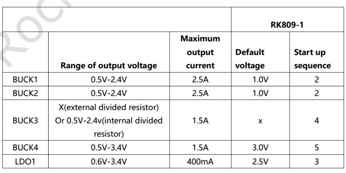
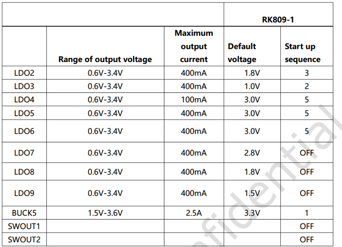
- Power-up sequencing: SoC platforms can require different rail sequences. The current sequences are shown below; consult the latest applicable datasheet for specifics.
Chinese PDF original · p10
Chinese PDF original · p10
Sequence table transcribed from the original image; blanks, x, OTP and ON/OFF are retained.
| Rail | Output range | Maximum current | Default voltage | Sequence |
|---|---|---|---|---|
| BUCK1 | 0.5V-2.4V | 2.5A | 1.0V | 2 |
| BUCK2 | 0.5V-2.4V | 2.5A | 1.0V | 2 |
| BUCK3 | X (external divider) / 0.5V-2.4V (internal divider) | 1.5A | x | 4 |
| BUCK4 | 0.5V-3.4V | 1.5A | 3.0V | 5 |
| LDO1 | 0.6V-3.4V | 400mA | 2.5V | 3 |
| LDO2 | 0.6V-3.4V | 400mA | 1.8V | 3 |
| LDO3 | 0.6V-3.4V | 400mA | 1.0V | 2 |
| LDO4 | 0.6V-3.4V | 100mA | 3.0V | 5 |
| LDO5 | 0.6V-3.4V | 400mA | 3.0V | 5 |
| LDO6 | 0.6V-3.4V | 400mA | 3.0V | 5 |
| LDO7 | 0.6V-3.4V | 400mA | 2.8V | OFF |
| LDO8 | 0.6V-3.4V | 400mA | 1.8V | OFF |
| LDO9 | 0.6V-3.4V | 400mA | 1.5V | OFF |
| BUCK5 | 1.5V-3.6V | 2.5A | 3.3V | 1 |
| SWOUT1 | OFF | |||
| SWOUT2 | OFF |
2. Configuration
2.1 Drivers and menuconfig
Kernel 4.4 configuration. RK809 driver files share some components with rk817 and rk805:
drivers/mfd/rk808.c
drivers/input/misc/rk8xx-pwrkey.c
drivers/rtc/rtc-rk808.c
drivers/gpio/gpio-rk8xx.c
drivers/regulator/rk808-regulator.c
drivers/clk/clk-rk808.c
Reference RK809 DTS file:
arch/arm64/boot/dts/rockchi/px30-evb-ddr4-v10.dts
Corresponding menuconfig symbols:
CONFIG_MFD_RK808
CONFIG_RTC_RK808
CONFIG_GPIO_RK8XX
CONFIG_REGULATOR_RK818
CONFIG_INPUT_RK8XX_PWRKEY
CONFIG_COMMON_CLK_RK808
Kernel 4.19 configuration. RK809 driver files:
drivers/mfd/rk808.c
drivers/input/misc/rk805-pwrkey.c       // 跟4.4内核不同
drivers/rtc/rtc-rk808.c
drivers/pinctrl/pinctrl-rk805.c         // 跟4.4内核不同
drivers/regulator/rk808-regulator.c     // 跟4.4内核不同
drivers/clk/clk-rk808.c
Reference RK809 DTS file:
arch/arm64/boot/dts/rockchi/px30-evb-ddr4-v10.dts
Corresponding menuconfig symbols:
CONFIG_MFD_RK808
CONFIG_RTC_RK808
CONFIG_PINCTRL_RK805
CONFIG_REGULATOR_RK808
CONFIG_INPUT_RK805_PWRKEY
CONFIG_COMMON_CLK_RK808
2.2 DTS configuration
Kernel 4.4 DTS configuration: i2c attachment, main properties, rtc, pwrkey, gpio and regulator.
&pinctrl {
    pmic {
        pmic_int: pmic_int {
            rockchip,pins =
                <0 RK_PA7 RK_FUNC_GPIO &pcfg_pull_up>;
        };
        soc_slppin_gpio: soc_slppin_gpio {
            rockchip,pins =
                <0 RK_PA4 RK_FUNC_GPIO &pcfg_output_low>;
        };
        soc_slppin_slp: soc_slppin_slp {
            rockchip,pins =
                <0 RK_PA4 RK_FUNC_1 &pcfg_pull_none>;
        };
        soc_slppin_rst: soc_slppin_rst {
            rockchip,pins =
                <0 RK_PA4 RK_FUNC_2 &pcfg_pull_none>;
        };
    };
};
&i2c1 {
    status = "okay";
    rk809: pmic@20 {
        compatible = "rockchip,rk809";
        reg = <0x20>;
        interrupt-parent = <&gpio0>;
        interrupts = <7 IRQ_TYPE_LEVEL_LOW>;
        pinctrl-names = "default", "pmic-sleep",
                "pmic-power-off", "pmic-reset";
        pinctrl-0 = <&pmic_int>;
        pinctrl-1 = <&soc_slppin_slp>, <&rk817_slppin_slp>;
        pinctrl-2 = <&soc_slppin_gpio>, <&rk817_slppin_pwrdn>;
        pinctrl-3 = <&soc_slppin_rst>, <&rk817_slppin_rst>;
        rockchip,system-power-controller;
        wakeup-source;
        #clock-cells = <1>;
        clock-output-names = "rk808-clkout1", "rk808-clkout2";
        //fb-inner-reg-idxs = <2>;
        /* 1: rst regs (default in codes), 0: rst the pmic */
        pmic-reset-func = <1>;
        vcc1-supply = <&vcc5v0_sys>;
        vcc2-supply = <&vcc5v0_sys>;
        vcc3-supply = <&vcc5v0_sys>;
        vcc4-supply = <&vcc5v0_sys>;
        vcc5-supply = <&vcc3v3_sys>;
        vcc6-supply = <&vcc3v3_sys>;
        vcc7-supply = <&vcc3v3_sys>;
        vcc8-supply = <&vcc3v3_sys>;
        vcc9-supply = <&vcc5v0_sys>;
        pwrkey {
    status = "okay";
};
pinctrl_rk8xx: pinctrl_rk8xx {
    gpio-controller;
    #gpio-cells = <2>;
    rk817_slppin_null: rk817_slppin_null {
        pins = "gpio_slp";
        function = "pin_fun0";
    };
    rk817_slppin_slp: rk817_slppin_slp {
        pins = "gpio_slp";
        function = "pin_fun1";
    };
    rk817_slppin_pwrdn: rk817_slppin_pwrdn {
        pins = "gpio_slp";
        function = "pin_fun2";
    };
    rk817_slppin_rst: rk817_slppin_rst {
        pins = "gpio_slp";
        function = "pin_fun3";
    };
};
regulators {
    vdd_logic: DCDC_REG1 {
        regulator-always-on;
        regulator-boot-on;
        regulator-min-microvolt = <950000>;
        regulator-max-microvolt = <1350000>;
        regulator-ramp-delay = <6001>;
        regulator-initial-mode = <0x2>;
        regulator-name = "vdd_logic";
        regulator-state-mem {
            regulator-on-in-suspend;
            regulator-suspend-microvolt = <950000>;
        };
    };
    vdd_arm: DCDC_REG2 {
        regulator-always-on;
        regulator-boot-on;
        regulator-min-microvolt = <950000>;
        regulator-max-microvolt = <1350000>;
        regulator-ramp-delay = <6001>;
        regulator-initial-mode = <0x2>;
        regulator-name = "vdd_arm";
        regulator-state-mem {
            regulator-off-in-suspend;
            regulator-suspend-microvolt = <950000>;
        };
    };
            vcc_ddr: RK809_DCDC3@2 {
                .................
            };
            .............................
        };
        rk809_codec: codec {
            #sound-dai-cells = <0>;
            compatible = "rockchip,rk809-codec", "rockchip,rk817-codec";
            clocks = <&cru SCLK_I2S1_OUT>;
            clock-names = "mclk";
            pinctrl-names = "default";
            pinctrl-0 = <&i2s1_2ch_mclk>;
            hp-volume = <20>;
            spk-volume = <3>;
            status = "okay";
        };
    };
};
-
i2c attachment: place the complete RK809 node under the corresponding i2c node and set
status = "okay";. -
Main properties — do not change the following:
compatible = "rockchip,rk809";
reg = <0x20>;
rockchip,system-power-controller;
wakeup-source;
gpio-controller;
#gpio-cells = <2>;
Configurable according to pinctrl rules:
- interrupt-parent: GPIO controller owning pmic_int.
- interrupts: pin index and polarity of pmic_int on that controller.
- pinctrl-names: do not modify; fixed as “default”.
- pinctrl-0: reference to the pmic_int pin defined in pinctrl.
-
rtc, pwrkey and gpio: when selected in menuconfig but not needed, add the corresponding nodes in DTS and explicitly set
status = "disabled". The drivers will not load; resulting boot error logs may be ignored in this case. To enable them, remove the nodes or setstatus = "okay". -
regulator
-
regulator-compatible: Name required for driver matching; changing it causes loading to fail. -
regulator-name: Supply name; match the schematic. regulator_get uses this name. -
regulator-init-microvolt: Initial voltage in U-Boot; ineffective in the kernel. -
regulator-min-microvolt: Minimum adjustable voltage during operation. -
regulator-max-microvolt: Maximum adjustable voltage during operation. -
regulator-initial-mode: DCDC runtime mode, normally 1: 1 = force PWM; 2 = auto PWM/PFM. -
regulator-mode: DCDC suspend mode, normally 2: 1 = force PWM; 2 = auto PWM/PFM. -
regulator-initial-state: Suspend state; must be 3. -
regulator-boot-on: Enable the rail when registering the regulator. -
regulator-always-on: Disallow disabling the rail during operation and enable it at registration. -
regulator-ramp-delay: DCDC voltage rise time; source fixed value 12500. -
regulator-on-in-suspend: Keep powered during suspend; replace with regulator-off-in-suspend to power off. -
regulator-suspend-microvolt: Standby voltage when the rail remains powered.
- power off: RK809 can shut down directly through an I/O signal. The kernel registers pm_shutdown_prepare_fn for preparation, primarily disabling RTC interrupts and configuring special-I/O IOMUX. The source says actual shutdown occurs “in PCIE”, where pm_power_off directly changes the I/O to power off.
static int rk817_shutdown_prepare(struct rk808 *rk808)
{
    int ret;

    /* close rtc int when power off */
    regmap_update_bits(rk808->regmap,
               RK817_INT_STS_MSK_REG1,
               (0x3 << 5), (0x3 << 5));
    regmap_update_bits(rk808->regmap,
               RK817_RTC_INT_REG,
               (0x3 << 2), (0x0 << 2));

    if (rk808->pins && rk808->pins->p && rk808->pins->power_off) {
        ret = regmap_update_bits(rk808->regmap,
                     RK817_SYS_CFG(3),
                     RK817_SLPPIN_FUNC_MSK,
                     SLPPIN_NULL_FUN);
        if (ret) {
            pr_err("shutdown: config SLPPIN_NULL_FUN error!\n");
            return 0;
        }

        ret = regmap_update_bits(rk808->regmap,
                     RK817_SYS_CFG(3),
                     RK817_SLPPOL_MSK,
                     RK817_SLPPOL_H);
        if (ret) {
            pr_err("shutdown: config RK817_SLPPOL_H error!\n");
            return 0;
        }
        ret = pinctrl_select_state(rk808->pins->p,
                       rk808->pins->power_off);
        if (ret)
            pr_info("%s:failed to activate pwroff state\n",
                __func__);
        else
            return ret;
    }

    /* pmic sleep shutdown function */
    ret = regmap_update_bits(rk808->regmap,
                 RK817_SYS_CFG(3),
                 RK817_SLPPIN_FUNC_MSK, SLPPIN_DN_FUN);
    return ret;
}
- clk: a node using a RK809 clock references it as follows:
clocks = <&rk809 1>;
First argument: &rk809, fixed. Second argument: clock index, only 0 or 1; 0 = rk809-clkout1, 1 = rk809-clkout2.
Kernel 4.19 DTS configuration
See the kernel 4.4 DTS configuration. Difference: kernel 4.19 no longer needs a gpio child node, but other modules still reference RK809 pins using gpios = <&rk809 0 GPIO_ACTIVE_LOW>;.
2.3 Function interfaces
The following interfaces cover common regulator operations: enable, disable, set voltage and get voltage.
- Get a regulator:
struct regulator *regulator_get(struct device *dev, const char *id)
Use NULL for dev by default; id matches regulator-name in DTS.
- Release regulator:
void regulator_put(struct regulator *regulator)
- Enable regulator:
int regulator_enable(struct regulator *regulator)
- Disable regulator:
int regulator_disable(struct regulator *regulator)
- Get voltage regulator:
int regulator_get_voltage(struct regulator *regulator)
- Set regulator voltage:
int regulator_set_voltage(struct regulator *regulator, int min_uV, int max_uV)
The caller must ensure min_uV = max_uV.
- Example
struct regulator *rdev_logic;

rdev_logic = regulator_get(NULL, "vdd_logic");      // 获取vdd_logic
regulator_enable(rdev_logic);               // 使能vdd_logic
regulator_set_voltage(rdev_logic, 1100000, 1100000);    // 设置电压1.1v
regulator_disable(rdev_logic);              // 关闭vdd_logic
regulator_put(rdev_logic);              // 释放vdd_logic
Kernel 4.4 and 4.19 also provide regulator interfaces prefixed devm_ to manage allocated resources for developers.
3. Debug
3.1 kernel
Command format is unchanged from kernel 3.10; only the path differs. Kernel 4.4 uses /sys/rk8xx/rk8xx_dbg.
3.2 kernel
Refer to the kernel 4.4 commands.