
Source RK-KF-YF-199 V1.0.0, RK806, Linux 5.10. Covers PMIC submodules, concepts, functions, DTS and issue diagnosis. Platform reference only: verify the ArmSoM board PMIC, SoC, SDK/BSP, kernel, supplies and wiring. No ArmSoM hardware validation. Only a Chinese source is available; all four languages use its original figures, including any embedded English labels. No corresponding English PDF exists in this batch. Hardware commands are documented, not executed.
1. Basics
1.1 Overview
RK806 integrates 10 high-current DCDCs, 5 NLDOs, 6 PLDOs and adjustable power-on sequencing. System supplies are generally DCDC and LDO, with the following properties (consult detailed references separately).
- DCDC: high efficiency at large input/output voltage differences, but high ripple and cost; suitable for large voltage differences and high-current loads. PWM has good ripple transient response but lower efficiency; PFM is efficient but has limited load capability.
- PLDO: like previous PMIC LDOs, input minimum 2.0V and maximum 5.5V.
- NLDO: supports low input/output voltages and lower loss, e.g. 1.1V input and 0.9V output.
1.2 Functions
RK806 functions fall into three groups:
- Regulator: control each DCDC/LDO power state.
- GPIO: three IOs can put the entire PMIC into standby, independently control standby of assigned supplies, or serve as ordinary GPIOs.
- Pwrkey: detect power-button press/release and save one AP GPIO.
1.3 Chip pin functions
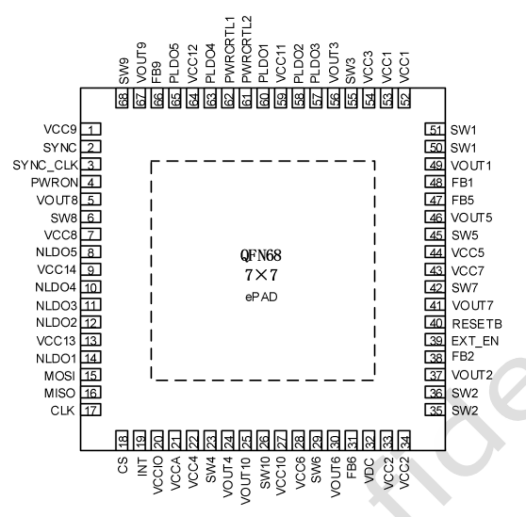
Original figure from Chinese PDF — p.5
Pay particular attention to SLEEP and INT in the following description.
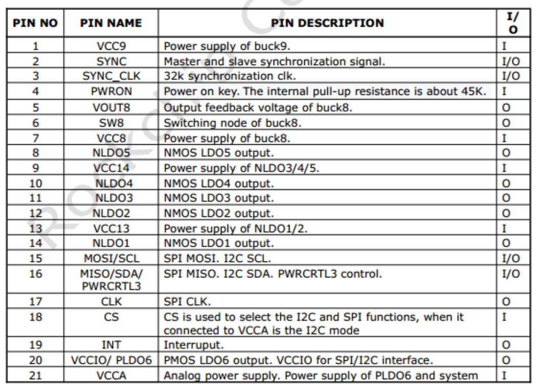
Original figure from Chinese PDF — p.6
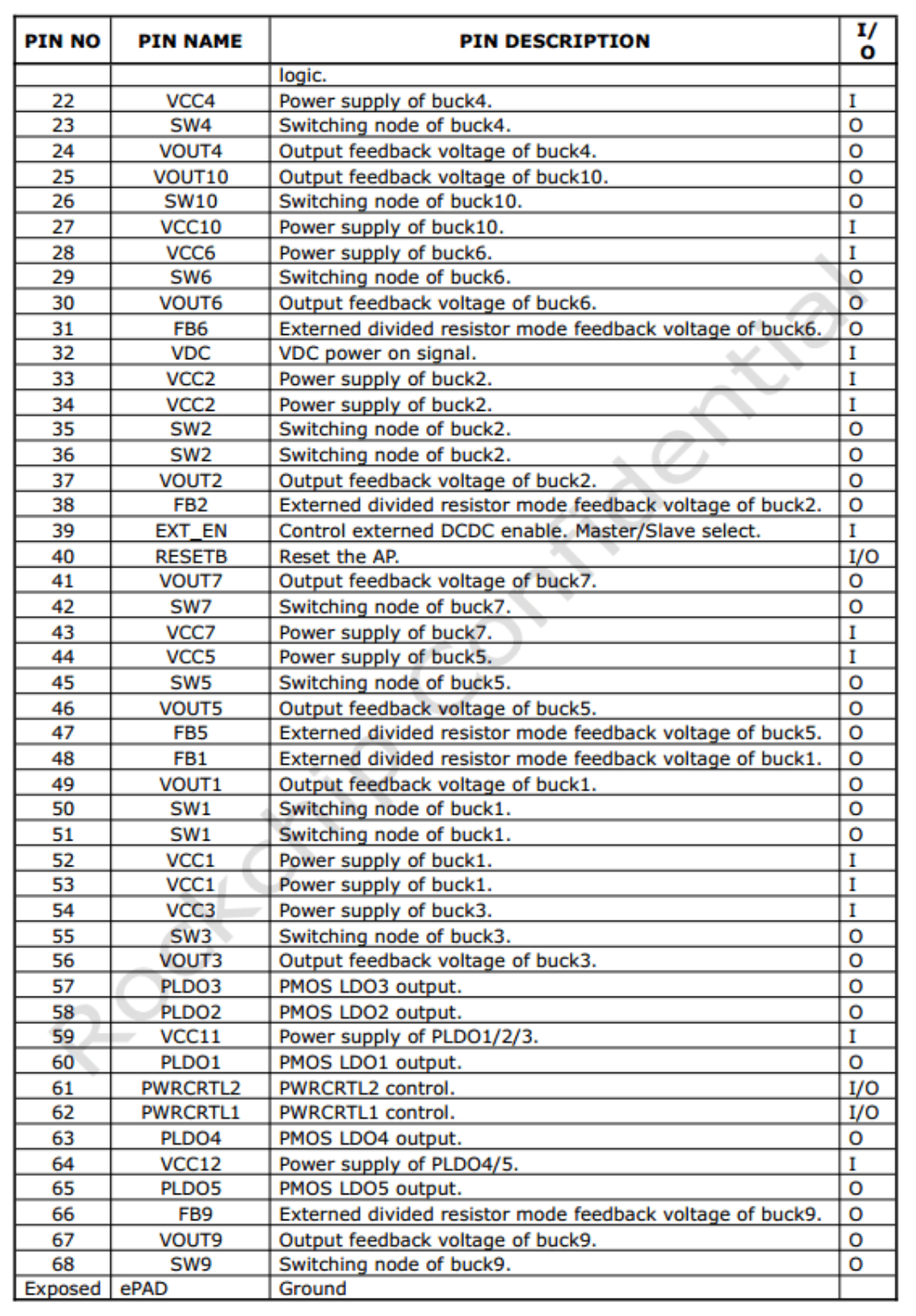
Original figure from Chinese PDF — p.7
Pin definitions (transcribed row by row from the figures above; source names and I/O markers retained)
| Pin No. | Pin name | Description | I/O |
|---|---|---|---|
| 1 | VCC9 | Power supply of buck9 | I |
| 2 | SYNC | Master/slave synchronization signal | I/O |
| 3 | SYNC_CLK | 32k synchronization clk | I/O |
| 4 | PWRON | Power on key; internal pull-up about 45K | I |
| 5 | VOUT8 | Output feedback voltage of buck8 | O |
| 6 | SW8 | Switching node of buck8 | O |
| 7 | VCC8 | Power supply of buck8 | I |
| 8 | NLDO5 | NMOS LDO5 output | O |
| 9 | VCC14 | Power supply of NLDO3/4/5 | I |
| 10 | NLDO4 | NMOS LDO4 output | O |
| 11 | NLDO3 | NMOS LDO3 output | O |
| 12 | NLDO2 | NMOS LDO2 output | O |
| 13 | VCC13 | Power supply of NLDO1/2 | I |
| 14 | NLDO1 | NMOS LDO1 output | O |
| 15 | MOSI/SCL | SPI MOSI, I2C SCL | I/O |
| 16 | MISO/SDA/PWRCRTL3 | SPI MISO, I2C SDA, PWRCRTL3 control | I/O |
| 17 | CLK | SPI CLK | O |
| 18 | CS | Select I2C/SPI; connected to VCCA selects I2C | I |
| 19 | INT | Interrupt | O |
| 20 | VCCIO/PLDO6 | PMOS LDO6 output; VCCIO for SPI/I2C interface | O |
| 21 | VCCA | Analog supply; power supply of PLDO6 and system logic | I |
| 22 | VCC4 | Power supply of buck4 | I |
| 23 | SW4 | Switching node of buck4 | O |
| 24 | VOUT4 | Output feedback voltage of buck4 | O |
| 25 | VOUT10 | Output feedback voltage of buck10 | O |
| 26 | SW10 | Switching node of buck10 | O |
| 27 | VCC10 | Power supply of buck10 | I |
| 28 | VCC6 | Power supply of buck6 | I |
| 29 | SW6 | Switching node of buck6 | O |
| 30 | VOUT6 | Output feedback voltage of buck6 | O |
| 31 | FB6 | External divider resistor mode feedback voltage of buck6 | O |
| 32 | VDC | VDC power on signal | I |
| 33 | VCC2 | Power supply of buck2 | I |
| 34 | VCC2 | Power supply of buck2 | I |
| 35 | SW2 | Switching node of buck2 | O |
| 36 | SW2 | Switching node of buck2 | O |
| 37 | VOUT2 | Output feedback voltage of buck2 | O |
| 38 | FB2 | External divider resistor mode feedback voltage of buck2 | O |
| 39 | EXT_EN | Control extended DCDC enable; Master/Slave select | I |
| 40 | RESETB | Reset AP | I/O |
| 41 | VOUT7 | Output feedback voltage of buck7 | O |
| 42 | SW7 | Switching node of buck7 | O |
| 43 | VCC7 | Power supply of buck7 | I |
| 44 | VCC5 | Power supply of buck5 | I |
| 45 | SW5 | Switching node of buck5 | O |
| 46 | VOUT5 | Output feedback voltage of buck5 | O |
| 47 | FB5 | External divider resistor mode feedback voltage of buck5 | O |
| 48 | FB1 | External divider resistor mode feedback voltage of buck1 | O |
| 49 | VOUT1 | Output feedback voltage of buck1 | O |
| 50 | SW1 | Switching node of buck1 | O |
| 51 | SW1 | Switching node of buck1 | O |
| 52 | VCC1 | Power supply of buck1 | I |
| 53 | VCC1 | Power supply of buck1 | I |
| 54 | VCC3 | Power supply of buck3 | I |
| 55 | SW3 | Switching node of buck3 | O |
| 56 | VOUT3 | Output feedback voltage of buck3 | O |
| 57 | PLDO3 | PMOS LDO3 output | O |
| 58 | PLDO2 | PMOS LDO2 output | O |
| 59 | VCC11 | Power supply of PLDO1/2/3 | I |
| 60 | PLDO1 | PMOS LDO1 output | O |
| 61 | PWRCRTL2 | PWRCRTL2 control | I/O |
| 62 | PWRCRTL1 | PWRCRTL1 control | I/O |
| 63 | PLDO4 | PMOS LDO4 output | O |
| 64 | VCC12 | Power supply of PLDO4/5 | I |
| 65 | PLDO5 | PMOS LDO5 output | O |
| 66 | FB9 | External divider resistor mode feedback voltage of buck9 | O |
| 67 | VOUT9 | Output feedback voltage of buck9 | O |
| 68 | SW9 | Switching node of buck9 | O |
| Exposed | ePAD | Ground |
1.4 Important concepts
SPI and I2C communication are supported by the chip. The documented software supports SPI only, with default SPI frequency 1M. PMIC has three operating modes.
- Normal mode: during normal operation, the active level of pmic_sleep is configurable.
- Sleep mode: lower standby consumption by reducing selected outputs or disabling supplies according to the product requirements. AP configures pmic_sleep for sleep via SPI, then raises it; on SoC wake-up it returns low and PMIC exits sleep.
- Shutdown: AP configures pmic_sleep through SPI and raises it to turn off system power.
- int: normally high, low during an interrupt until handled.
- pwrcrtl1/pwrcrtl2/pwrcrtl3: usable as ordinary GPIOs. The source says “these two pins” despite listing three; retain this discrepancy for verification.
- pwron: connect the power button for press/release detection.
- DCDC: PWM (force PWM), PFM and AUTO switching. AUTO is efficient but worse for ripple transient response. Runtime uses PWM for stability; sleep uses AUTO PWM/PFM.
- PLDO6: supplies PMIC/AP VCCIO. These IOs require power whenever used, at least 1.8V; PLDO6 therefore normally must not be below 1.8V or be disabled in standby.
- DCDC/LDO runtime voltage ranges follow.
- DCDC voltage range is discontinuous:
| Voltage range(V) | Step(mV) | Values(V) |
|---|---|---|
| 0.7125 ~ 1.45 | 6.25 | 0.5、0.50625、 …… 1.5 |
| 1.5~ 3.4 | 25 | 1.5、1.525、…… 3.4 |
- NLDO/PLDO voltage range is continuous:
| Voltage range(V) | Step(mV) | Values(V) |
|---|---|---|
| 0.5 ~ 3.4 | 12.5 | 0.5125、0.525、…… 3.4 |
1.5 Dual-PMIC operation
Master/slave is determined by EXT_EN at first power-on: EXT_EN shorted to VCCA selects Slave; floating or pulled down selects Master. For two RK806s connect SYNC_CLK and SYNC between the chips. Master supplies SYNC_CLK near 32K; Slave receives it. SYNC pulses synchronize power-on, power-off, reset and sequencing.
Connect the Master/Slave PWRON pins together and RESETB pins together for power-on enable and external reset-button input. VDC pins may be connected together, or Slave VDC may connect to Master EXT_EN.
2. Configuration
2.1 Driver and menuconfig
RK806 driver files:
drivers/mfd/rk806-core.c
drivers/mfd/rk806-spi.c
drivers/pinctrl/pinctrl-rk806.c
drivers/regulator/rk806-regulator.c
Corresponding menuconfig options:
CONFIG_PINCTRL_RK806=y
CONFIG_MFD_RK806_SPI=y
CONFIG_REGULATOR_RK806=y
2.2 DTS configuration
Kernel 5.10 DTS includes SPI attachment, GPIO and regulator. Single-RK806 DTS:
&pinctrl {
         pmic {
                soc_slppin_gpio: soc_slppin_gpio {
                        rockchip,pins = <0 RK_PA2
                                RK_FUNC_GPIO &pcfg_output_low>;
                };
                soc_slppin_shutdown: soc_slppin_shutdown {
                        rockchip,pins = <0 RK_PA2
                                RK_FUNC_GPIO &pcfg_output_high>;
                };
        };
};

&spi2 {
        status = "okay";
        assigned-clocks = <&cru CLK_SPI2>;
        assigned-clock-rates = <200000000>;
        num-cs = <&spi2 {
        status = "okay";
        assigned-clocks = <&cru CLK_SPI2>;
        assigned-clock-rates = <200000000>;
        num-cs = <2>;

        rk806single@0 {
                compatible = "rockchip,rk806";
                spi-max-frequency = <1000000>;
                reg = <0x0>;

                interrupt-parent = <&gpio0>;
                interrupts = <7 IRQ_TYPE_LEVEL_LOW>;

                pinctrl-names = "default", "pmic-sleep", "pmic-power-off", "pmic-reset";
                pinctrl-0 = <&soc_slppin_gpio>, <&rk806_dvs1_null>, <&rk806_dvs2_null>, <&rk806_dvs3_null>;
                pinctrl-1 = <&soc_slppin_gpio>, <&rk806_dvs1_slp>, <&rk806_dvs2_null>, <&rk806_dvs3_null>;
                pinctrl-2 = <&rk806_dvs1_pwrdn>, <&rk806_dvs2_null>, <&rk806_dvs3_null>;
                pinctrl-3 = <&rk806_dvs1_rst>, <&rk806_dvs2_null>, <&rk806_dvs3_null>;

                /* 2800mv-3500mv */
                low_voltage_threshold = <3000>;
                /* 2700mv-3400mv */
                shutdown_voltage_threshold = <2700>;
                /* 140 160 */
                shutdown_temperture_threshold = <160>;
                hotdie_temperture_threshold = <115>;

                /* 0: restart PMU;
                 * 1: reset all the power off reset registers,
                 *    forcing the state to switch to ACTIVE mode;
                 * 2: Reset all the power off reset registers,
                 *    forcing the state to switch to ACTIVE mode,
                 *    and simultaneously pull down the RESETB PIN for 5mS before releasing
                 */
                pmic-reset-func = <1>;

                vcc1-supply = <&vcc5v0_sys>;
                vcc2-supply = <&vcc5v0_sys>;
                vcc3-supply = <&vcc5v0_sys>;
                vcc4-supply = <&vcc5v0_sys>;
                vcc5-supply = <&vcc5v0_sys>;
                vcc6-supply = <&vcc5v0_sys>;
                vcc7-supply = <&vcc5v0_sys>;
                vcc8-supply = <&vcc5v0_sys>;
                vcc9-supply = <&vcc5v0_sys>;
                vcc10-supply = <&vcc5v0_sys>;
                vcc11-supply = <&vcc_2v0_pldo_s3>;
                vcc12-supply = <&vcc5v0_sys>;
                vcc13-supply = <&vcc_1v1_nldo_s3>;
                vcc14-supply = <&vcc_1v1_nldo_s3>;
                vcca-supply = <&vcc5v0_sys>;2>;

                regulators {
                        vdd_gpu_s0: vdd_gpu_mem_s0: DCDC_REG1 {
                                regulator-always-on;
                                regulator-boot-on;
                                regulator-min-microvolt = <550000>;
                                regulator-max-microvolt = <950000>;
                                regulator-ramp-delay = <12500>;
                                regulator-name = "vdd_gpu_s0";
                                regulator-state-mem {
                                        regulator-off-in-suspend;
                                };
                        };

                        vdd_cpu_lit_s0: vdd_cpu_lit_mem_s0: DCDC_REG2 {
                                regulator-always-on;
                                regulator-boot-on;
                                regulator-min-microvolt = <550000>;
                                regulator-max-microvolt = <950000>;
                                regulator-ramp-delay = <12500>;
                                regulator-name = "vdd_cpu_lit_s0";
                                regulator-state-mem {
                                        regulator-off-in-suspend;
                                };
                        };

                        vdd_log_s0: DCDC_REG3 {
                            .................
                        };

                        vdd_vdenc_s0: vdd_vdenc_mem_s0: DCDC_REG4 {
                            .................
                       };
                       .............................
               };
        };
};
Dual-RK806 DTS:
&pinctrl {
    pmic {
            soc_slppin_gpio: soc_slppin_gpio {
                    rockchip,pins = <0 RK_PA2
                            RK_FUNC_GPIO &pcfg_output_low>;
            };
            soc_slppin_shutdown: soc_slppin_shutdown {
                    rockchip,pins = <0 RK_PA2
                            RK_FUNC_GPIO &pcfg_output_high>;
            };
    };
};

&spi2 {
        status = "okay";
        assigned-clocks = <&cru CLK_SPI2>;
        assigned-clock-rates = <200000000>;
        num-cs = <2>;
        rk806master@0 {
                compatible = "rockchip,rk806";
                spi-max-frequency = <1000000>;
                reg = <0x0>;

                interrupt-parent = <&gpio0>;
                interrupts = <7 IRQ_TYPE_LEVEL_LOW>;
                /* 0: restart PMU;
                 * 1: reset all the power off reset registers,
                 *    forcing the state to switch to ACTIVE mode;
                 * 2: Reset all the power off reset registers,
                 *    forcing the state to switch to ACTIVE mode,
                 *    and simultaneously pull down the RESETB PIN for 5mS before releasing
                 */
                pmic-reset-func = <1>;

                vcc1-supply = <&vcc5v0_sys>;
                vcc2-supply = <&vcc5v0_sys>;
                .................
                vcca-supply = <&vcc5v0_sys>;
                regulators {
                        vdd_gpu_s0: DCDC_REG1 {
                                regulator-always-on;
                                regulator-boot-on;
                                regulator-min-microvolt = <550000>;
                                regulator-max-microvolt = <950000>;
                                regulator-ramp-delay = <12500>;
                                regulator-name = "vdd_gpu_s0";
                                regulator-state-mem {
                                        regulator-off-in-suspend;
                                };
                      };
                        vdd_npu_s0: DCDC_REG2 {
                        .................
                        };
                        .................
              };
       };
       rk806slave@1 {
                compatible = "rockchip,rk806";
                spi-max-frequency = <1000000>;
                reg = <0x01>;

                interrupt-parent = <&gpio0>;
                interrupts = <7 IRQ_TYPE_LEVEL_LOW>;
                /* 0: restart PMU;
                 * 1: reset all the power off reset registers,
                 *    forcing the state to switch to ACTIVE mode;
                 * 2: Reset all the power off reset registers,
                 *    forcing the state to switch to ACTIVE mode,
                 *    and simultaneously pull down the RESETB PIN for 5mS before releasing
               */
                pmic-reset-func = <1>;

                vcc1-supply = <&vcc5v0_sys>;
                vcc2-supply = <&vcc5v0_sys>;
                .................
                vcca-supply = <&vcc5v0_sys>;

                pwrkey {
                        status = "disabled";
                };
                regulators {
                        vdd_cpu_big1_s0: DCDC_REG1 {
                                regulator-always-on;
                                regulator-boot-on;
                                regulator-min-microvolt = <550000>;
                                regulator-max-microvolt = <950000>;
                                regulator-ramp-delay = <12500>;
                                regulator-name = "vdd_cpu_big1_s0";
                                regulator-state-mem {
                                        regulator-off-in-suspend;
                                };
                        };
                        vdd_cpu_big0_s0: DCDC_REG2 {
                        .................
                        };
                        .................
                };
       };
};
- Attach the complete rk806 node below its SPI node and set status = “okay”.
- Main node: the following must not be modified.
compatible = "rockchip,rk806";
spi-max-frequency = <1000000>;
reg = <0x0>;

interrupt-parent = <&gpio0>;
interrupts = <7 IRQ_TYPE_LEVEL_LOW>;
Editable, following pinctrl rules: interrupt-parent selects the GPIO controller of pmic_int; interrupts defines its pin index and polarity within that controller.
- pwrkey/gpio: if unused, add these DTS nodes with status = “disabled”. Drivers will not be enabled; resulting boot error logs may be ignored.
pwrkey {
        status = "disabled";
};
- Regulator:
- regulator-compatible: registration match name; cannot change, or loading fails.
- regulator-name: supply name, preferably matching hardware; regulator_get uses it.
- regulator-init-microvolt: u-boot initial voltage, ineffective in kernel.
- regulator-min-microvolt / regulator-max-microvolt: runtime minimum/maximum.
- regulator-initial-mode: runtime DCDC mode, usually 1; 1 force pwm, 2 auto pwm/pfm.
- regulator-mode: sleep DCDC mode, usually 2; same values.
- regulator-initial-state: suspend mode, must be 3.
- regulator-boot-on: enable at registration.
- regulator-always-on: forbid runtime shutdown and enable at registration.
- regulator-ramp-delay: DCDC voltage rise time, fixed 12500.
- regulator-on-in-suspend: keep power during sleep; replace with regulator-off-in-suspend to turn off.
- regulator-suspend-microvolt: standby voltage if power stays on.
Kernel 5.10 configuration: refer to the kernel 5.10 DTS configuration above.
2.3 Function interfaces
The following interfaces cover ordinary regulator on/off, voltage setting and reading.
- Get regulator:
struct regulator *devm_regulator_get_optional(struct device *dev, const char *id). dev is the current device; id corresponds to the DTS -supply property.
- Release: void regulator_put(struct regulator *regulator)
- Enable: int regulator_enable(struct regulator *regulator)
- Disable: int regulator_disable(struct regulator *regulator)
- Get regulator voltage
int regulator_get_voltage(struct regulator *regulator)
- Set voltage:
int regulator_set_voltage(struct regulator *regulator, int min_uV, int max_uV). Caller must ensure min_uV <= max_uV.
- Example
struct regulator *vdd_ana;

vdd_ana = devm_regulator_get_optional(dev, "power");
/* 从dts获取power-supply
   power-supply = <&vcc3v3_lcd0_n> */
regulator_enable(vdd_ana);
regulator_disable(vdd_ana);                         // 关闭vdd_ana
regulator_put(vdd_ana);                             // 释放vdd_ana
3. Debugging
3.1 Kernel
PMIC driver logic is simple; final register settings are central. A common debugging entry is /sys/kernel/debug/regulator.
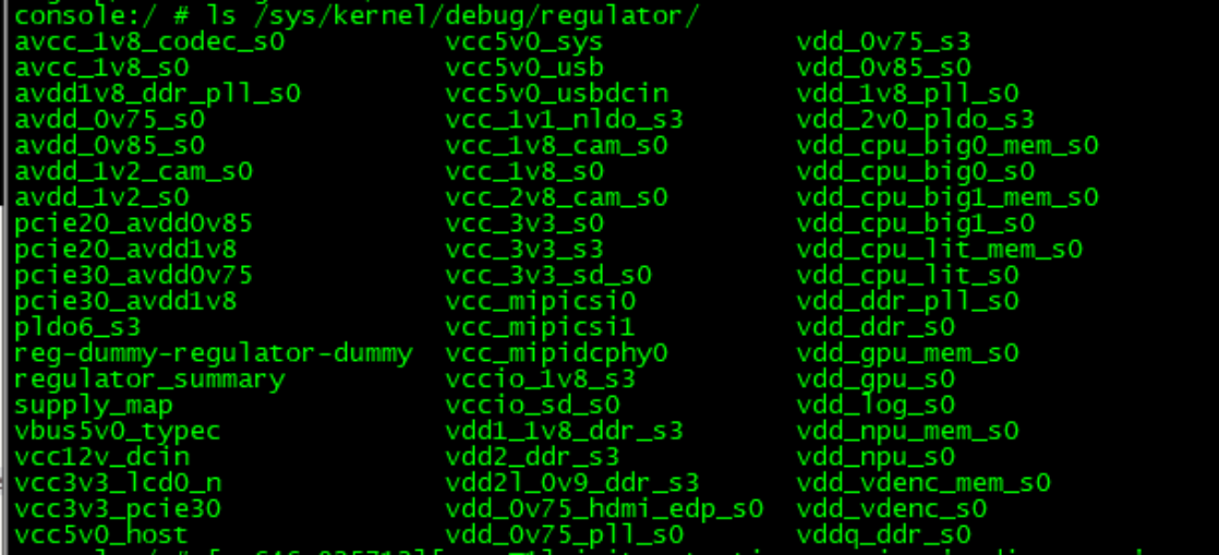
Transcription of legible source-image content (source example; unreadable clipped edge fragments are not guessed):
console:/ # ls /sys/kernel/debug/regulator/
avcc_1v8_codec_s0         vcc5v0_sys             vdd_0v75_s3
avcc_1v8_s0               vcc5v0_usb             vdd_0v85_s0
avdd1v8_ddr_pll_s0        vcc5v0_usbdcin         vdd_1v8_pll_s0
avdd_0v75_s0              vcc_1v1_nldo_s3        vdd_2v0_pldo_s3
avdd_0v85_s0              vcc_1v8_cam_s0         vdd_cpu_big0_mem_s0
avdd_1v2_cam_s0           vcc_1v8_s0             vdd_cpu_big0_s0
avdd_1v2_s0               vcc_2v8_cam_s0         vdd_cpu_big1_mem_s0
pcie20_avdd0v85           vcc_3v3_s0             vdd_cpu_big1_s0
pcie20_avdd1v8            vcc_3v3_s3             vdd_cpu_lit_mem_s0
pcie30_avdd0v75           vcc_3v3_sd_s0          vdd_cpu_lit_s0
pcie30_avdd1v8            vcc_mipicsi0           vdd_ddr_pll_s0
pldo6_s3                  vcc_mipicsi1           vdd_ddr_s0
reg-dummy-regulator-dummy vcc_mipidcphy0         vdd_gpu_mem_s0
regulator_summary        vccio_1v8_s3           vdd_gpu_s0
supply_map               vccio_sd_s0            vdd_log_s0
vbus5v0_typec             vdd1_1v8_ddr_s3        vdd_npu_mem_s0
vcc12v_dcin               vdd2_ddr_s3            vdd_npu_s0
vcc3v3_lcd0_n             vdd21_0v9_ddr_s3       vdd_vdenc_mem_s0
vcc3v3_pcie30             vdd_0v75_hdmi_edp_s0   vdd_vdenc_s0
vcc5v0_host               vdd_0v75_pll_s0        vddq_ddr_s0
Original figure from Chinese PDF — p.15
/sys/kernel/debug/regulator/regulator_summary
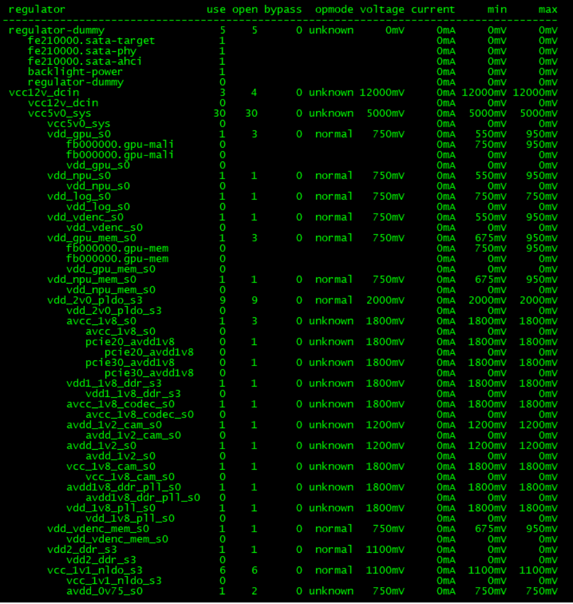
Transcription of legible source-image content (source example; unreadable clipped edge fragments are not guessed):
 regulator                    use open bypass opmode  voltage current min max
 regulator-dummy                5 5 0 unknown 0mV 0mA 0mV 0mV
    fe210000.sata-target         1                 0mA 0mV 0mV
    fe210000.sata-phy            1                 0mA 0mV 0mV
    fe210000.sata-ahci           1                 0mA 0mV 0mV
    backlight-power             1                 0mA 0mV 0mV
    regulator-dummy             0                 0mA 0mV 0mV
 vcc12v_dcin                    3 4 0 unknown 12000mV 0mA 12000mV 12000mV
    vcc12v_dcin                  0                 0mA 0mV 0mV
    vcc5v0_sys                  30 30 0 unknown 5000mV 0mA 5000mV 5000mV
       vcc5v0_sys                0                 0mA 0mV 0mV
       vdd_gpu_s0                1 3 0 normal 750mV 0mA 550mV 950mV
          fb000000.gpu-mali      0                 0mA 750mV 950mV
          fb000000.gpu-mali      0                 0mA 0mV 0mV
          vdd_gpu_s0             0                 0mA 0mV 0mV
       vdd_npu_s0                1 1 0 normal 750mV 0mA 550mV 950mV
          vdd_npu_s0             0                 0mA 0mV 0mV
       vdd_log_s0                1 1 0 normal 750mV 0mA 750mV 750mV
          vdd_log_s0             0                 0mA 0mV 0mV
       vdd_vdenc_s0              1 1 0 normal 750mV 0mA 550mV 950mV
          vdd_vdenc_s0           0                 0mA 0mV 0mV
       vdd_gpu_mem_s0            1 3 0 normal 750mV 0mA 675mV 950mV
          fb000000.gpu-mem       0                 0mA 750mV 950mV
          fb000000.gpu-mem       0                 0mA 0mV 0mV
          vdd_gpu_mem_s0         0                 0mA 0mV 0mV
       vdd_npu_mem_s0            1 1 0 normal 750mV 0mA 675mV 950mV
          vdd_npu_mem_s0         0                 0mA 0mV 0mV
       vdd_2v0_pldo_s3           9 9 0 normal 2000mV 0mA 2000mV 2000mV
          vdd_2v0_pldo_s3        0                 0mA 0mV 0mV
          avcc_1v8_s0            1 3 0 unknown 1800mV 0mA 1800mV 1800mV
             avcc_1v8_s0         0                 0mA 0mV 0mV
             pcie20_avdd1v8      0 1 0 unknown 1800mV 0mA 1800mV 1800mV
                pcie20_avdd1v8   0                 0mA 0mV 0mV
             pcie30_avdd1v8      0 1 0 unknown 1800mV 0mA 1800mV 1800mV
                pcie30_avdd1v8   0                 0mA 0mV 0mV
          vdd1_1v8_ddr_s3        1 1 0 unknown 1800mV 0mA 1800mV 1800mV
             vdd1_1v8_ddr_s3     0                 0mA 0mV 0mV
          avcc_1v8_codec_s0      1 1 0 unknown 1800mV 0mA 1800mV 1800mV
             avcc_1v8_codec_s0   0                 0mA 0mV 0mV
          avdd_1v2_cam_s0        1 1 0 unknown 1200mV 0mA 1200mV 1200mV
             avdd_1v2_cam_s0     0                 0mA 0mV 0mV
          avdd_1v2_s0            1 1 0 unknown 1200mV 0mA 1200mV 1200mV
             avdd_1v2_s0         0                 0mA 0mV 0mV
          vcc_1v8_cam_s0         1 1 0 unknown 1800mV 0mA 1800mV 1800mV
             vcc_1v8_cam_s0      0                 0mA 0mV 0mV
          avdd1v8_ddr_pll_s0     1 1 0 unknown 1800mV 0mA 1800mV 1800mV
             avdd1v8_ddr_pll_s0  0                 0mA 0mV 0mV
          vdd_1v8_pll_s0         1 1 0 unknown 1800mV 0mA 1800mV 1800mV
             vdd_1v8_pll_s0      0                 0mA 0mV 0mV
       vdd_vdenc_mem_s0          1 1 0 normal 750mV 0mA 675mV 950mV
          vdd_vdenc_mem_s0       0                 0mA 0mV 0mV
       vdd2_ddr_s3               1 1 0 normal 1100mV 0mA 0mV 0mV
          vdd2_ddr_s3            0                 0mA 0mV 0mV
       vcc_1v1_nldo_s3           6 6 0 normal 1100mV 0mA 1100mV 1100mV
          vcc_1v1_nldo_s3        0                 0mA 0mV 0mV
       avdd_0v75_s0              1 2 0 unknown 750mV 0mA 750mV 750mV
Original figure from Chinese PDF — p.16
Each supply’s properties and voltage values can be found through the following node:

Transcription of legible source-image content (source example; unreadable clipped edge fragments are not guessed):
console:/sys/kernel/debug/regulator/vdd_gpu_mem_s0 # ls
bypass_count  fb000000.gpu-mem  mode        vdd_gpu_mem_s0
consumers     force_disable   open_count  voltage
enable        load            use_count
Original figure from Chinese PDF — p.16
3.2 Kernel 5.10
Refer to the kernel 5.10 commands.
Editorial note: the source BUCK table states 0.7125–1.45 but lists 0.5–1.5; the NLDO range starts at 0.5 but its first listed value is 0.5125. The prose describes three PWRCTRL pins but also says two. Pin names use PWRCRTL, and SPI CLK is marked O. All are retained without speculative corrections; verify before adaptation.
Source DTS caveat: page 9 literally ends with num-cs = <&spi2 {, followed by repeated SPI properties; page 12 also contains a full-width semicolon. This is not a directly compilable complete DTS. These source issues are retained rather than guessed; verify against the corresponding BSP source. The original section 3.1 heading says only “Kernel”, without a version.