
This is a Rockchip RK3588 platform reference for Linux kernel 5.10 as specified by the source. For an ArmSoM project, verify the board SoC, exposed display interface, panel/bridge VRR capabilities and SDK/BSP patches. This does not establish support on every ArmSoM board. No ArmSoM hardware validation was performed; logs, waveforms, photographs and test descriptions are source examples.
Source: Rockchip_RK3588_Developer_Guide_Vsync_Adjust_CN.pdf, V1.2.0, 11 pages. Only the Chinese original was supplied. All three articles use its original figures; English and Russian translate the complete body and localize captions/alt text, retaining original labels inside figures.
Editorial notes · ArmSoM documentation · Rockchip
1. Scan timing
A frame is normally sent to the screen using the scan timing illustrated below:
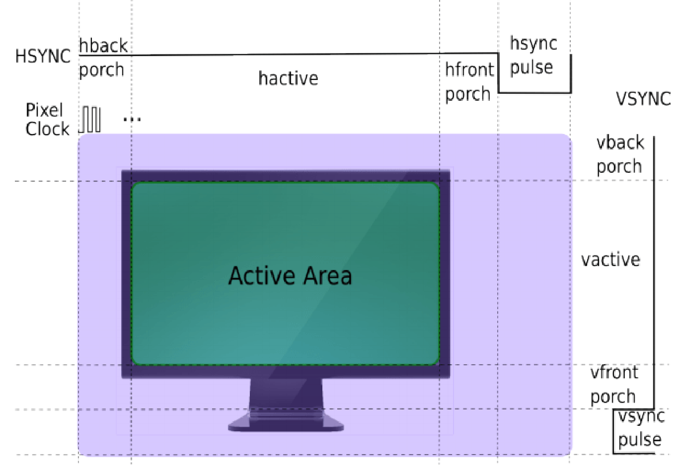
Scan timing and active display area
Each line consists of hsync, hback porch, hactive and hfront porch. Each frame consists of vsync, vback porch, vactive and vfront porch.
htotal is defined as follows:
htotal = hsync + hbackporch + hactive + hfrontporch
vtotal is defined as follows:
vtotal = vsync + vbackporch + vactive + vfrontporch
For scan output with pixel clock pixel_clk and refresh rate fps, the following relationship must hold:
pixel_clk = htotal * vtotal * fps
The scan diagram shows that one Vsync period equals 1/fps. Changing the Vsync period therefore means changing fps, which can be done by changing pixel clock, htotal or vtotal. For a fixed resolution,
hactive and vactive remain unchanged. Within htotal only hbank (hsync + hback porch + hfront porch) can be adjusted; within vtotal only vbank (vsync + vback porch + vfront porch) can be adjusted.
For the panels encountered in the source, hbank adjustment generally means adjusting HFP (hfront porch), while vbank adjustment generally means adjusting VFP (vfront porch). On RK3588, pixel-clock adjustment corresponds to dclk rate adjustment.
The following discussion of Vsync-period adjustment covers only VFP, HFP and dclk rate.
2. Display paths
The RK3588 display paths are shown below:
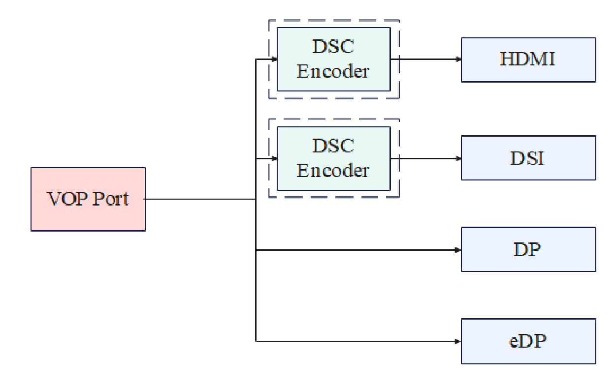
RK3588 display paths and optional DSC
HDMI, DSI, DP and eDP outputs are supported. HDMI and DSI output may use DSC. When evaluating Vsync-period adjustment for DSI and HDMI, consider DSC-enabled and DSC-disabled operation separately.
3. VOP adjustment
RK3588 VOP registers allow VFP, HFP or dclk rate to be adjusted. VFP changes can be configured to take effect immediately or at a frame boundary. HFP and dclk rate changes can only take effect at a frame boundary.
Changing the Vsync period through dclk rate has these restrictions:
1. Only VP0 and VP2 can change the Vsync period by switching the dclk source.
2. VP0 can switch between dclk0 and dclk1; VP2 can switch between dclk2 and dclk1.
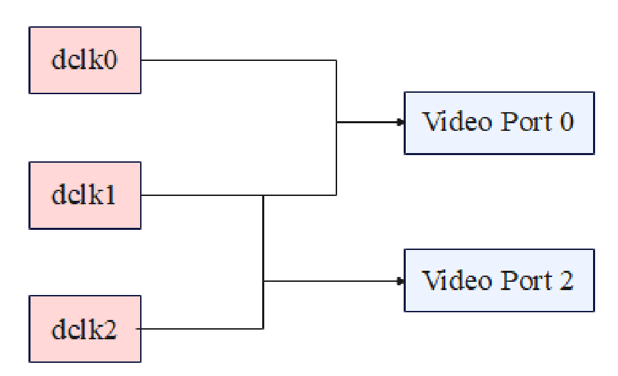
dclk source switching for VP0/VP2
For example, DSI connected to VP2 can implement dynamic 120/60fps switching. Its resolution information is:
console:/ # cat /sys/kernel/debug/dri/0/summary
Video Port0: DISABLED
Video Port1: DISABLED

Video Port2: ACTIVE
   Connector: DSI-1
      bus_format[1018]: RGB101010_1X30
      overlay_mode[0] output_mode[f] color_space[0], eotf:0
   Display mode: 3024x2016p120
      clk[1187744] real_clk[1187744] type[48] flag[a]
      H: 3024 4416 4432 4532
      V: 2016 2042 2044 2184
   Variable refresh rate info:
      Min refresh rate: 60
      Max refresh rate: 120
      Current refresh rate: 60

      Type: DCLK
      Current pixel clock:593872
   Cluster1-win0: ACTIVE
      win_id: 2
      format: AB24 little-endian (0x34324241)[AFBC] SDR[0] color_space[0]
glb_alpha[0xff]
      rotate: xmirror: 0 ymirror: 0 rotate_90: 0 rotate_270: 0
      csc: y2r[0] r2y[0] csc mode[0]
      zpos: 0
      src: pos[0, 0] rect[3024 x 2016]
      dst: pos[0, 0] rect[3024 x 2016]
      buf[0]: addr: 0x00000000ef7b9000 pitch: 12096 offset: 0
Video Port3: DISABLED
For 120/60fps switching, connect both dclk1 and dclk2 to v0pll. Their frequencies differ by a factor of two, allowing exact division while keeping the parent PLL stable. The clock relationship is:
cat /sys/kernel/debug/clk/clk_summary

...

   pll_v0pll          1  1  0 1187743988 0 0  50000
     v0pll            2  2  0 1187743988 0 0  50000
       dclk_vop2_src  1  2  0  296935997 0 0  50000
         dclk_vop2    1  2  0  296935997 0 0  50000
       dclk_vop1_src  1  2  0  148467999 0 0  50000
         dclk_vop1    1  2  0  148467999 0 0  50000
...
4. DSC adjustment
DSC supports adjustment of VFP and HFP, but both can only take effect immediately. DSC mode also accepts the timing supplied by VOP after a dclk adjustment.
5. DSI adjustment
DSI register changes take effect immediately, including both VFP and HFP. DSI has Manual and Auto-Calculation modes. In Auto-Calculation mode, the controller extracts all required information and timing parameters from the IPI and PPI interfaces to satisfy video-mode frame timing. IPI frames may change dynamically and the controller adapts its output frames. DSI can therefore automatically adjust PHY output to the received VOP timing without reconfiguring DSI registers. The supported adjustment methods differ between modes.
5.1 VFP adjustment
DSI can change its Vsync period by adjusting VFP.
In Manual mode, when the Vsync interrupt arrives, change the VFP registers of VOP, DSC (if enabled) and DSI together with immediate effect. This changes VFP for the current frame. DSI register limitations restrict VFP to a maximum of 1023.
To obtain a larger VFP, it is possible to change only the VFP registers of VOP and DSC (if DSC compression is used). However, leaving DSI VFP unchanged affects packet transmission during VFP, as shown below:
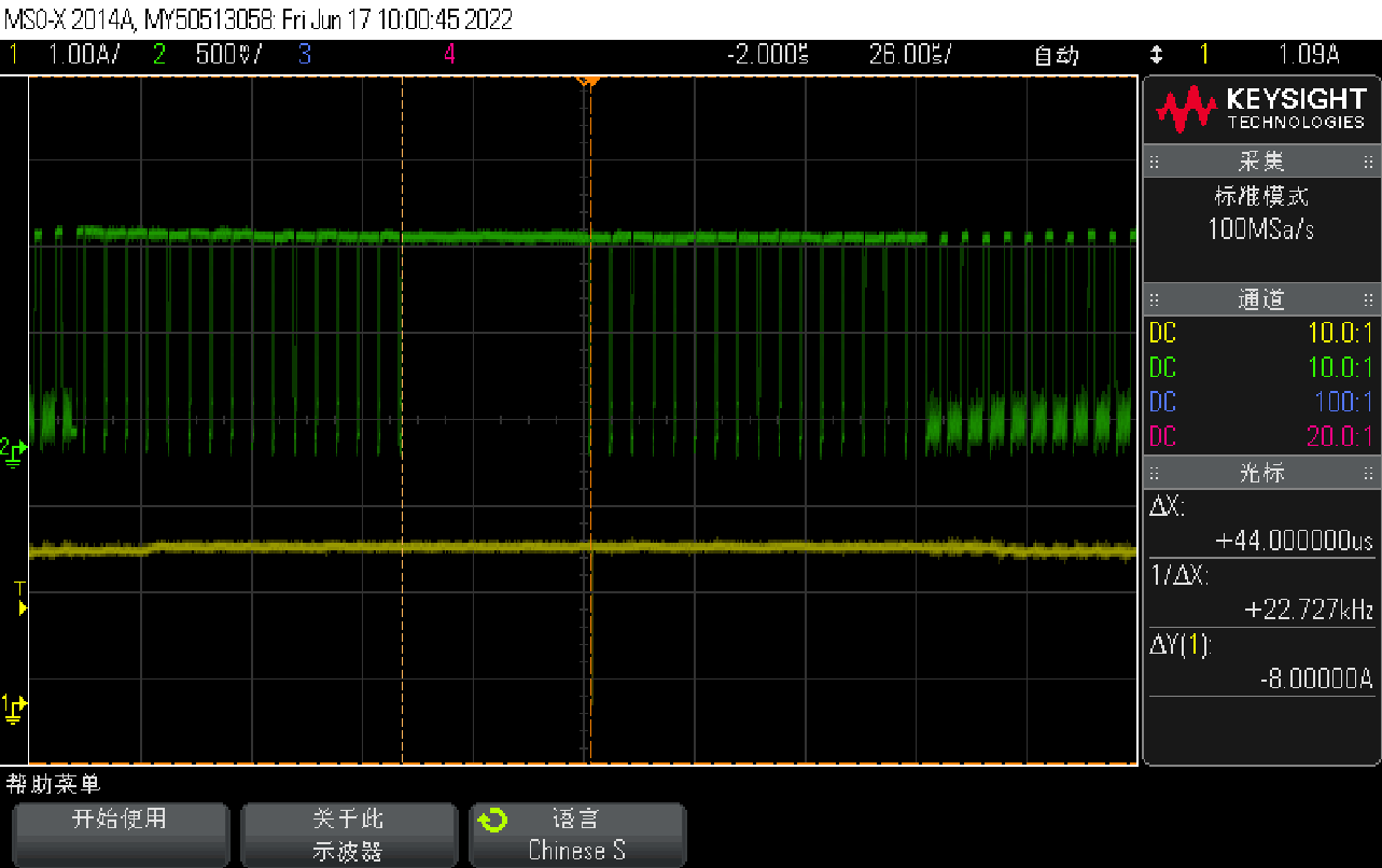
Source waveform: missing synchronization packets when DSI VFP is unchanged
Synchronization packets are missing. If the panel does not accept this waveform, display anomalies may occur. Leaving DSI VFP unconfigured is therefore not recommended.
In Auto-Calculation mode, only VOP and DSC (if enabled) need to be changed together with immediate effect when the Vsync interrupt arrives. DSI VFP is still limited to 1023.
5.2 HFP adjustment
Risks of implementing dynamic frame rates by configuring the DSC HFP register:
DSC timing registers take effect immediately, unlike VOP’s frame-boundary mechanism. Changing DSC registers at the end of a frame disrupts the current frame timing and introduces a frame-time error. DSC video mode requires VOP and DSC scan timings to match as closely as possible; otherwise the internal DSC buffer overflows.
The following abnormal MIPI DPHY waveform shows a DSC error with no data transmitted:
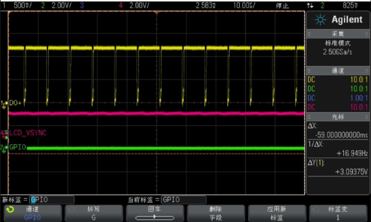
No MIPI DPHY data transmission after a DSC error
In Manual mode, RK3588 DSI currently does not support changing Vsync through HFP. The source’s local DSC-mode test produced the display anomaly shown below; this is not an ArmSoM test.
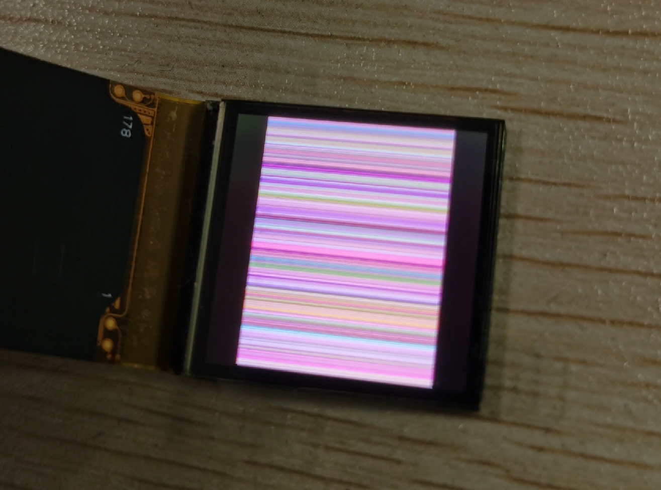
Source photograph of a display anomaly after HFP adjustment in DSC mode
In Auto-Calculation mode without DSC, only VOP HFP needs to be changed, and DSI supports this method. With DSC enabled, VOP and DSC registers must both be changed, but there is no guarantee that HFP changes take effect on the same line. HFP adjustment is therefore unsupported in that case.
5.3 dclk rate adjustment
Manual mode does not support changing the Vsync period through VOP dclk rate adjustment.
Auto-Calculation mode supports Vsync-period adjustment through dclk rate whether or not DSC is enabled. The DSI controller automatically adapts its output.
The two 120/60fps timing sets A/B in the red rectangle below illustrate frame-rate switching:
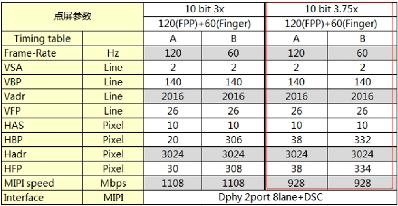
Two 120/60fps timing sets; red rectangle: 10 bit 3.75x A/B
| Parameter | Unit | 10 bit 3x A | 10 bit 3x B | 10 bit 3.75x A | 10 bit 3.75x B |
|---|---|---|---|---|---|
| Timing | 120(FPP)+60(Finger) | A | B | A | B |
| Frame-Rate | Hz | 120 | 60 | 120 | 60 |
| VSA | Line | 2 | 2 | 2 | 2 |
| VBP | Line | 140 | 140 | 140 | 140 |
| Vadr | Line | 2016 | 2016 | 2016 | 2016 |
| VFP | Line | 26 | 26 | 26 | 26 |
| HAS | Pixel | 10 | 10 | 10 | 10 |
| HBP | Pixel | 20 | 306 | 38 | 332 |
| Hadr | Pixel | 3024 | 3024 | 3024 | 3024 |
| HFP | Pixel | 30 | 308 | 38 | 334 |
| MIPI speed | Mbps | 1108 | 1108 | 928 | 928 |
| Interface | MIPI | Dphy 2port 8lane+DSC | Dphy 2port 8lane+DSC | Dphy 2port 8lane+DSC | Dphy 2port 8lane+DSC |
5.3.1 Details of frame switching through dclk rate
In the figure below, the red signal represents HSYNC information decoded inside the panel IC. A dclk-based frame-rate change takes effect at a frame boundary. At the transition, after counting 26 VFP lines from the preceding frame, the panel expects VSYNC, followed by 140+2 lines of VBP+VSA before DATA. The panel IC uses the average width of the first 4 lines after VSYNC and the transition time to determine the frame-rate switch.
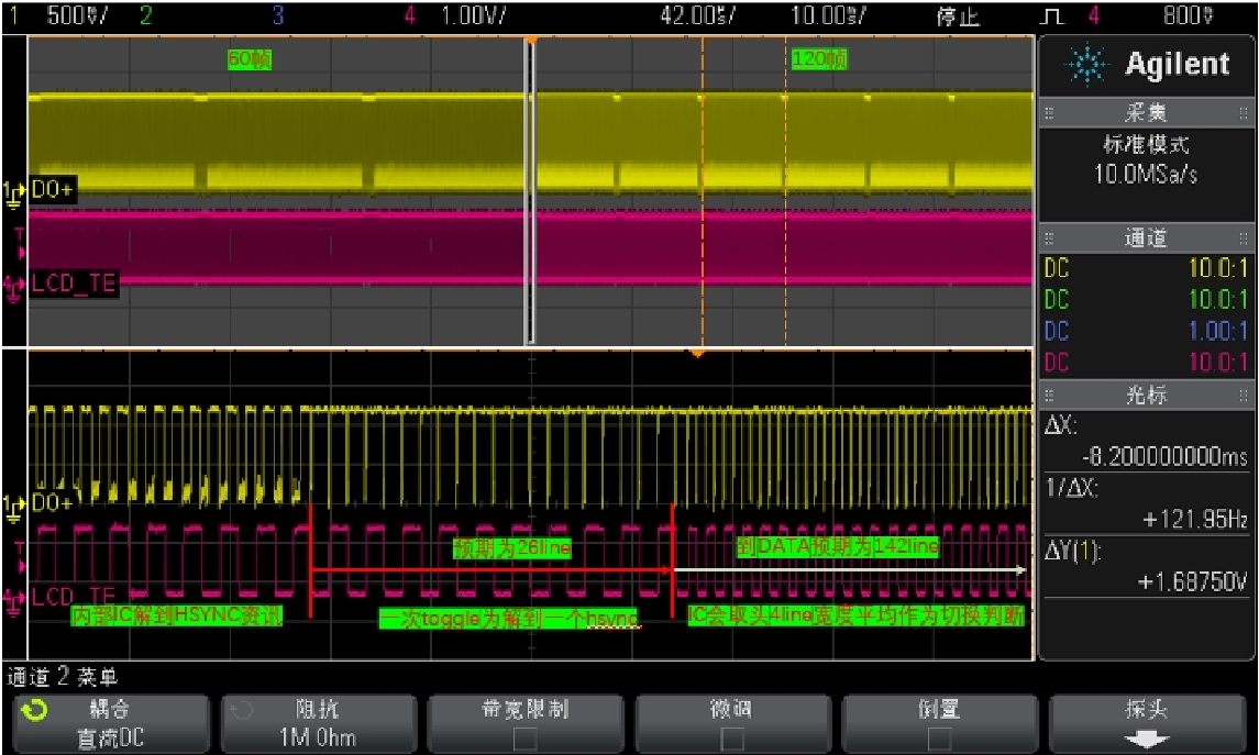
Source 60→120fps waveform. Green labels identify internal HSYNC, one toggle per hsync, 26 lines of the preceding frame, 142 lines before DATA, and mean line width over four lines.
5.3.2 From 120fps to 60fps
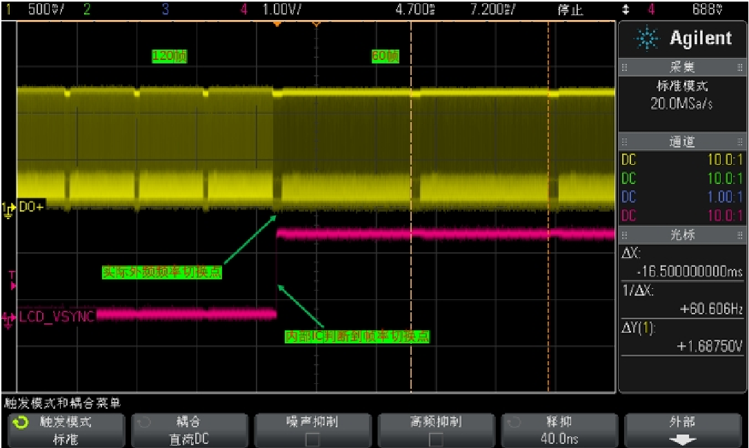
120→60fps: actual external-frequency switch and the switch detected by the internal IC
5.3.3 From 60fps to 120fps
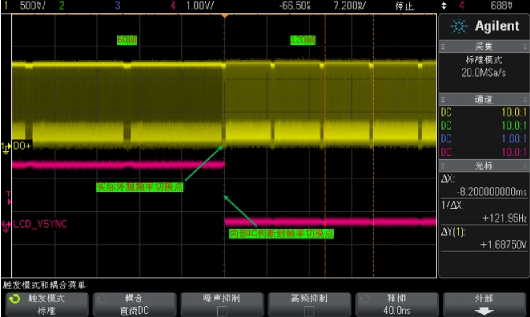
60→120fps: actual external-frequency switch and the switch detected by the internal IC
6. eDP/DP adjustment
VRR on eDP and DP requires support from the controller as well as the relevant DPCD/EDID descriptions. eDP/DP VRR support is also called Adaptive-Sync.
6.1 DPCD VRR support
MSA packets contain timing information used by the Sink to reconstruct video-stream timing. These timing parameters are intended for static video timing. If the stream timing changes dynamically, the Sink cannot use the MSA timing information. The Source reads MSA_TIMING_PAR_IGNORED in DOWN_STREAM_PORT_COUNT (DPCD address 00006h, bit6) to determine whether the Sink supports seamless timing changes (VRR). If supported and
the Source needs this feature, the source text refers to MSA_TIMING_PAR_IGNORE_EN in DOWNSPREAD_CTRL (DPCD address 00107h, bit7); the Sink ignores the MSA parameters shown below. The original sentence omits the exact write operation/value; it is not supplied by inference here.

Original table of MSA timing parameters that may be ignored
| HTotal[15:0] | HStart[15:0] | HSyncPolarity (HSP) | HSyncWidth[14:0] (HSW) |
|---|---|---|---|
| VTotal[15:0] | VStart[15:0] | VSyncPolarity (VSP) | VSyncWidth[14:0] (VSW) |
6.2 EDID VRR support
EDID defines the Display Range Limit Descriptor to describe VRR support, as shown below:
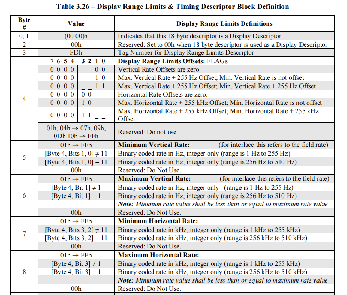
Original Display Range Limits descriptor excerpt; later bytes are not fully visible at the bottom of the source image
| Byte | Value / bits | Description |
|---|---|---|
| 0, 1 | (00 00)h | Identifies this 18-byte descriptor as a Display Descriptor. |
| 2 | 00h | Reserved: set to 00h when used as a Display Descriptor. |
| 3 | FDh | Display Range Limits Descriptor tag. |
| 4 | bits 7 6 5 4 3 2 1 0 | Display range offset flags. |
| 4 | 0000 –00 | Vertical rate offsets are zero. |
| 4 | 0000 –10 | Maximum vertical rate +255 Hz; minimum unchanged. |
| 4 | 0000 –11 | Maximum and minimum vertical rates +255 Hz. |
| 4 | 0000 00– | Horizontal rate offsets are zero. |
| 4 | 0000 10– | Maximum horizontal rate +255 kHz; minimum unchanged. |
| 4 | 0000 11– | Maximum and minimum horizontal rates +255 kHz. |
| 4 | 01h, 04h → 07h, 09h, 0Dh, 10h → FFh | Reserved; do not use. The original omits a separator between 0Dh and 10h; values are retained. |
| 5 | 01h → FFh | Minimum vertical rate (field rate for interlace) |
| 5 | Byte 4, bits 1, 0 ≠ 11 | Integer binary-coded rate, range 1 Hz ~ 255 Hz |
| 5 | Byte 4, bits 1, 0 = 11 | Integer binary-coded rate, range 256 Hz ~ 510 Hz |
| 5 | 00h | Reserved; do not use. |
| 6 | 01h → FFh | Maximum vertical rate (field rate for interlace) |
| 6 | Byte 4, bits 1 ≠ 1 | Integer binary-coded rate, range 1 Hz ~ 255 Hz |
| 6 | Byte 4, bits 1 = 1 | Integer binary-coded rate, range 256 Hz ~ 510 Hz |
| 6 | Note | Minimum rate must be less than or equal to maximum rate. |
| 6 | 00h | Reserved; do not use. |
| 7 | 01h → FFh | Minimum horizontal rate |
| 7 | Byte 4, bits 3, 2 ≠ 11 | Integer binary-coded rate, range 1 kHz ~ 255 kHz |
| 7 | Byte 4, bits 3, 2 = 11 | Integer binary-coded rate, range 256 kHz ~ 510 kHz |
| 7 | 00h | Reserved; do not use. |
| 8 | 01h → FFh | Maximum horizontal rate |
| 8 | Byte 4, bits 3 ≠ 1 | Integer binary-coded rate, range 1 kHz ~ 255 kHz |
| 8 | Byte 4, bits 3 = 1 | Integer binary-coded rate, range 256 kHz ~ 510 kHz |
| 8 | Note | Minimum rate must be less than or equal to maximum rate. |
| 8 | 00h | Reserved; do not use. |
This descriptor specifies the supported VRR range.
The source states that EDID timing definitions use minimum vblank and hblank. For example, if EDID gives a VRR range of 30 ~ 100 Hz, a timing with a 60Hz frame rate
supports VRR from 30 ~ 60Hz, whereas a 24 Hz timing does not support VRR. To reach lower frame rates within the specified VRR range, extend vbank.
6.3 eDP VRR adjustment
eDP supports Vsync adjustment through VFP. Only VOP VFP needs to be changed; configure analogix,force-stream-valid in the eDP DTS so that eDP automatically adapts to the timing sent by VOP.
An eDP panel may not support EDID. In that case, define the supported VRR range in DTS.