
This is a Rockchip RGB/MCU platform reference. The V1.7.1 support table lists RK1808, RK312X/PX3SE, RK3288, RK3308B/BS, RK3326/PX30, RK3506, RK3562, RK3568, RK3576, RV1103/1106, RV1109/RV1126 and RV1126B, with different capabilities. It does not establish support on every ArmSoM board. SPI/panel configurations distinguish kernel 4.19 and earlier from 5.10 and later. Verify the board SDK/BSP, exposed interface, pin multiplexing, voltage and panel timing. No ArmSoM hardware validation was performed; source values and illustrations are platform examples.
Source: Rockchip_Developer_Guide_RGB_MCU_CN.pdf, V1.7.1, 34 pages. Only Chinese was supplied. English/Russian translate the full technical body; all three versions use the Chinese PDF figures, without claiming translated image labels.
Editorial notes · ArmSoM documentation · Rockchip
1. Basic concepts
1.1 RGB interface
RGB is also called DPI (Display Pixel Interface). It uses four synchronization signals: Vsync, Hsync, Den (Enable) and DCLK (Dotclk). The synchronization method distinguishes DE mode from SYNC mode. Rockchip RGB output timing can support both.
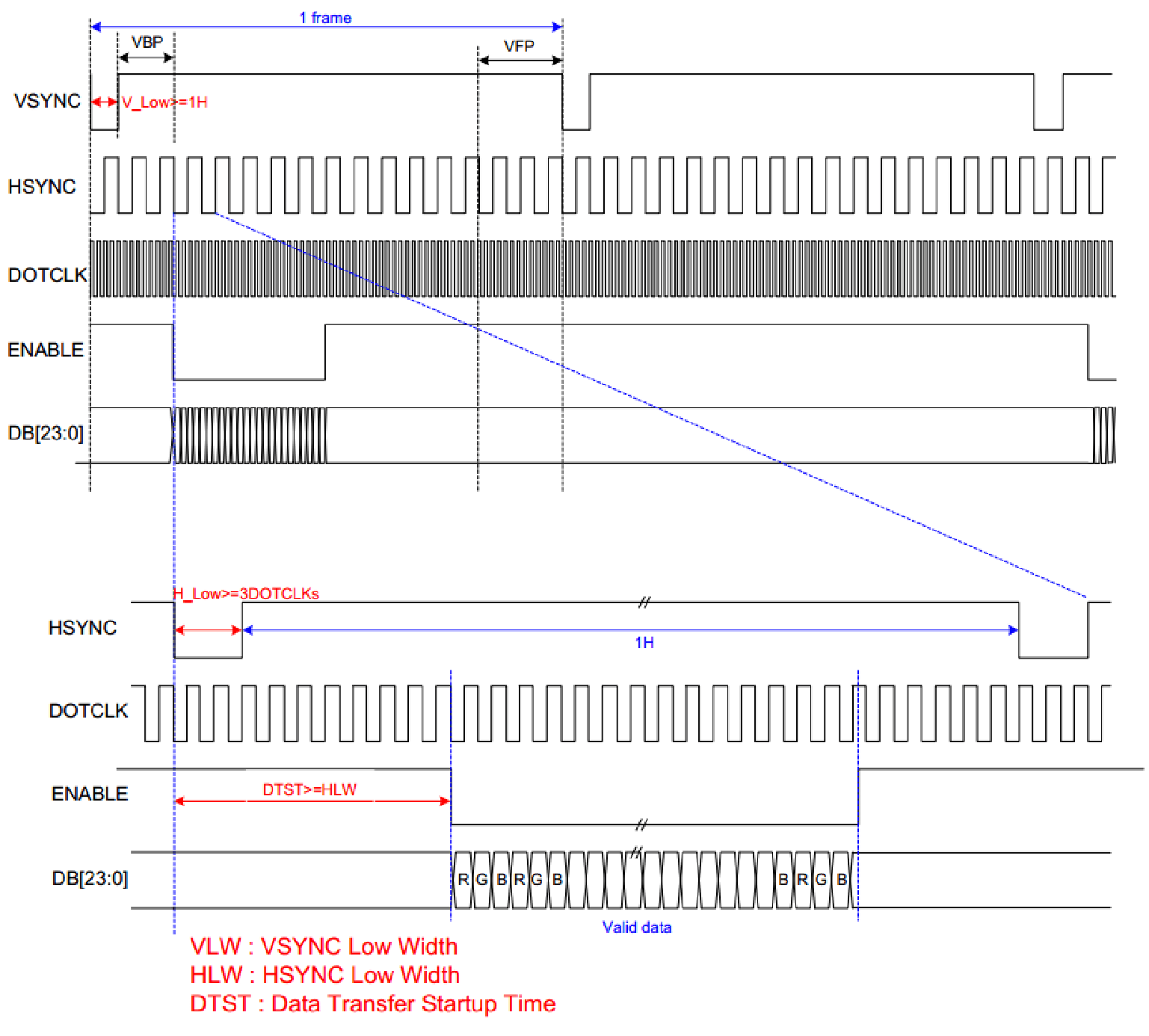
DE-mode timing
1.1.1 DE mode
The validity of DB[23:0] depends only on Den. The source states that data is valid at the low level and invalid otherwise.
1.1.2 SYNC mode
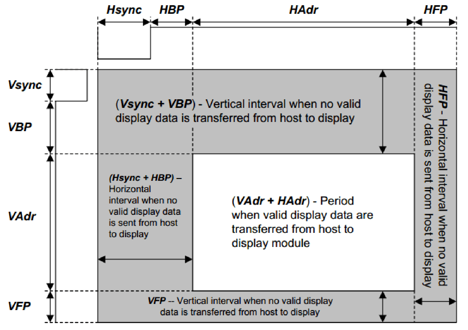
SYNC-mode timing
DB[23:0] data is synchronized by Vsync and Hsync and scanned according to the timing above.
1.2 MCU interface
MCU is also called DBI or the 8080 interface. It supports bidirectional communication between TX and RX, with four synchronization signals: RS (CSX), CSN (D/CX), WEN (WRX) and REN (RDX). This introductory source paragraph states that Rockchip supports only MCU TX; the later platform table separately lists read support for RK3506 and RV1126B. The inconsistency is retained for review.
1.2.1 Write timing
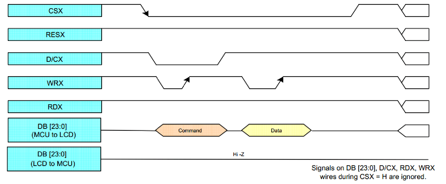
MCU write timing
CSX, D/CX and WRX are driven low in sequence. While DB[23:0] is valid, WRX first goes low and then high.
1.2.2 Read timing
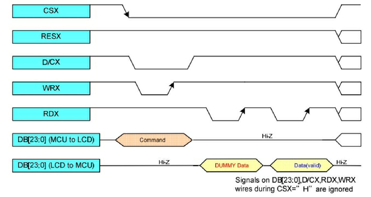
MCU read timing and initial dummy data
CSX, D/CX and RDX are driven low in sequence. While DB[23:0] is valid, RDX first goes low and then high.
Before reading, perform a write operation to send the register address to the panel.
The first read returns invalid data; valid data starts with the second read.
MCU read is commonly used for panel debugging, identifying panel IDs for multi-panel compatibility, and the frame-read feature described later.
1.2.3 Bypass and normal modes
Bypass mode is used when MCU and panel exchange commands through write/read operations.
Sending init/deinit commands from panel-init-sequence/panel-exit-sequence and performing frame write/read are bypass-mode operations. See the corresponding Software Configuration sections below.
In normal mode, the host sends image data through MCU into panel RAM for normal display. This mode normally starts after panel-init-sequence has been transmitted and successful panel initialization confirmed.
Bypass mode may include write and read operations; normal mode includes write operations only.
2. Rockchip platform support
| SoC platform | RGB support | MCU support | MCU read support | VOP version | Video Port path (VOP 2.0) | Supported output modes |
|---|---|---|---|---|---|---|
| RK1808 | Y | Y | N | VOP 1.0 | RGB666/RGB565 | |
| RK312X/PX3SE | Y | N | N | VOP 1.0 | RGB888/RGB666/RGB565 | |
| RK3288 | Y | Y | N | VOP 1.0 | RGB888/RGB666/RGB565/RGB3x8 | |
| RK3308B/RK3308BS | Y | Y | N | VOP 1.0 | RGB888/RGB666/RGB565/RGB3x8 | |
| RK3326/PX30 | Y | Y | N | VOP 1.0 | RGB888/RGB666/RGB565 | |
| RK3506 | Y | Y | Y | VOP 1.0 | RGB888/RGB666/RGB565/RGB3x8/RGB3x6/RGB2x8 | |
| RK3562 | Y | Y | N | VOP 2.0 | VP0 | RGB888/RGB666/RGB565/RGB3x8 |
| RK3568 | Y | N | N | VOP 2.0 | VP2 | RGB888/RGB666/RGB565 |
| RK3576 | Y | Y | N | VOP 2.0 | VP1/VP2 | RGB888/RGB666/RGB565/RGB3x8/RGB3x6/RGB2x8 |
| RV1103 | Y | Y | N | VOP 1.0 | RGB3x8 | |
| RV1106 | Y | Y | N | VOP 1.0 | RGB666/RGB565/RGB3x8 | |
| RV1109/RV1126 | Y | Y | N | VOP 1.0 | RGB888/RGB666/RGB565/RGB3x8 | |
| RV1126B | Y | Y | Y | VOP 1.0 | RGB888/RGB666/RGB565/RGB3x8/RGB3x6/RGB2x8 |
For VOP and VP (Video Port), refer to Rockchip_Developer_Guide_DRM_Display_Driver_CN.
3. Hardware connections
3.1 RK3562/RK3576/RK3506/RV1126B
| Component name | Pin name | RGB888 (MCU) | RGB666 (MCU) | RGB565 (MCU) | RGB3x8 (MCU) | RGB3x6 (MCU) | RGB2x8 (MCU) |
|---|---|---|---|---|---|---|---|
| DCLK | VO_LCDC_CLK | DCLK(RS) | DCLK(RS) | DCLK(RS) | DCLK(RS) | DCLK(RS) | DCLK(RS) |
| VSYNC | VO_LCDC_VSYNC | VSYNC(CSN) | VSYNC(CSN) | VSYNC(CSN) | VSYNC(CSN) | VSYNC(CSN) | VSYNC(CSN) |
| HSYNC | VO_LCDC_HSYNC | HSYNC(WRN) | HSYNC(WRN) | HSYNC(WRN) | HSYNC(WRN) | HSYNC(WRN) | HSYNC(WRN) |
| DEN | VO_LCDC_DEN | DEN(RDN) | DEN(RDN) | DEN(RDN) | DEN(RDN) | DEN(RDN) | DEN(RDN) |
| R7_D23 | VO_LCDC_D23 | √ | √ | √ | √ (D7_m1) | √ (D5_m1) | √ (D7_m1) |
| R6_D22 | VO_LCDC_D22 | √ | √ | √ | √ (D6_m1) | √ (D4_m1) | √ (D6_m1) |
| R5_D21 | VO_LCDC_D21 | √ | √ | √ | √ (D5_m1) | √ (D3_m1) | √ (D5_m1) |
| R4_D20 | VO_LCDC_D20 | √ | √ | √ | √ (D4_m1) | √ (D2_m1) | √ (D4_m1) |
| R3_D19 | VO_LCDC_D19 | √ | √ | √ | √ (D3_m1) | √ (D1_m1) | √ (D3_m1) |
| R2_D18 | VO_LCDC_D18 | √ | √ | × | × | × | × |
| R1_D17 | VO_LCDC_D17 | √ | × | × | × | × | × |
| R0_D16 | VO_LCDC_D16 | √ | × | × | × | × | × |
| G7_D15 | VO_LCDC_D15 | √ | √ | √ | √ (D2_m1) | √ (D0_m1) | √ (D2_m1) |
| G6_D14 | VO_LCDC_D14 | √ | √ | √ | √ (D1_m1) | × | √ (D1_m1) |
| G5_D13 | VO_LCDC_D13 | √ | √ | √ | √ (D0_m1) | × | √ (D0_m1) |
| G4_D12 | VO_LCDC_D12 | √ | √ | √ | √ (D7_m0) | √ (D5_m0) | √ (D7_m0) |
| G3_D11 | VO_LCDC_D11 | √ | √ | √ | √ (D6_m0) | √ (D4_m0) | √ (D6_m0) |
| G2_D10 | VO_LCDC_D10 | √ | √ | √ | √ (D5_m0) | √ (D3_m0) | √ (D5_m0) |
| G1_D9 | VO_LCDC_D9 | √ | × | × | × | × | × |
| G0_D8 | VO_LCDC_D8 | √ | × | × | × | × | × |
| B7_D7 | VO_LCDC_D7 | √ | √ | √ | √ (D4_m0) | √ (D2_m0) | √ (D4_m0) |
| B6_D6 | VO_LCDC_D6 | √ | √ | √ | √ (D3_m0) | √ (D1_m0) | √ (D3_m0) |
| B5_D5 | VO_LCDC_D5 | √ | √ | √ | √ (D2_m0) | √ (D0_m0) | √ (D2_m0) |
| B4_D4 | VO_LCDC_D4 | √ | √ | √ | √ (D1_m0) | × | √ (D1_m0) |
| B3_D3 | VO_LCDC_D3 | √ | √ | √ | √ (D0_m0) | × | √ (D0_m0) |
| B2_D2 | VO_LCDC_D2 | √ | √ | × | × | × | × |
| B1_D1 | VO_LCDC_D1 | √ | × | × | × | × | × |
| B0_D0 | VO_LCDC_D0 | √ | × | × | × | × | × |
3.2 RK3568
| Component name | Pin name | RGB888 | RGB666 | RGB565 |
|---|---|---|---|---|
| DCLK | LCDC_CLK | DCLK | DCLK | DCLK |
| VSYNC | LCDC_VSYNC | VSYNC | VSYNC | VSYNC |
| HSYNC | LCDC_HSYNC | HSYNC | HSYNC | HSYNC |
| DEN | LCDC_DEN | DEN | DEN | DEN |
| R7_D23 | LCDC_D23 | √ | √ | √ |
| R6_D22 | LCDC_D22 | √ | √ | √ |
| R5_D21 | LCDC_D21 | √ | √ | √ |
| R4_D20 | LCDC_D20 | √ | √ | √ |
| R3_D19 | LCDC_D19 | √ | √ | √ |
| R2_D18 | LCDC_D18 | √ | √ | × |
| R1_D17 | LCDC_D17 | √ | × | × |
| R0_D16 | LCDC_D16 | √ | × | × |
| G7_D15 | LCDC_D15 | √ | √ | √ |
| G6_D14 | LCDC_D14 | √ | √ | √ |
| G5_D13 | LCDC_D13 | √ | √ | √ |
| G4_D12 | LCDC_D12 | √ | √ | √ |
| G3_D11 | LCDC_D11 | √ | √ | √ |
| G2_D10 | LCDC_D10 | √ | √ | √ |
| G1_D9 | LCDC_D9 | √ | × | × |
| G0_D8 | LCDC_D8 | √ | × | × |
| B7_D7 | LCDC_D7 | √ | √ | √ |
| B6_D6 | LCDC_D6 | √ | √ | √ |
| B5_D5 | LCDC_D5 | √ | √ | √ |
| B4_D4 | LCDC_D4 | √ | √ | √ |
| B3_D3 | LCDC_D3 | √ | √ | √ |
| B2_D2 | LCDC_D2 | √ | √ | × |
| B1_D1 | LCDC_D1 | √ | × | × |
| B0_D0 | LCDC_D0 | √ | × | × |
3.3 RK312X/PX3SE/RK3288/RK3308B/RK3308BS/RK3328/RK3326/PX30/RV1109/RV1126
| Component name | Pin name | RGB888 (MCU) | RGB666 (MCU) | RGB666_CPADHI (MCU) | RGB565 (MCU) | RGB565_CPADHI (MCU) | RGB3x8 (MCU) |
|---|---|---|---|---|---|---|---|
| DCLK | LCDC_CLK/LCD_CLK | DCLK(RS) | DCLK(RS) | DCLK(RS) | DCLK(RS) | DCLK(RS) | DCLK(RS) |
| VSYNC | LCDC_VSYNC/LCD_VSYNC | VSYNC(CSN) | VSYNC(CSN) | VSYNC(CSN) | VSYNC(CSN) | VSYNC(CSN) | VSYNC(CSN) |
| HSYNC | LCDC_HSYNC/LCD_HSYNC | HSYNC(WRN) | HSYNC(WRN) | HSYNC(WRN) | HSYNC(WRN) | HSYNC(WRN) | HSYNC(WRN) |
| DEN | LCDC_DEN/LCD_DEN | DEN(RDN) | DEN(RDN) | DEN(RDN) | DEN(RDN) | DEN(RDN) | DEN(RDN) |
| R7_D23 | LCDC_D23/LCD_D23 | √ | × | √ | × | √ | × |
| R6_D22 | LCDC_D22/LCD_D22 | √ | × | √ | × | √ | × |
| R5_D21 | LCDC_D21/LCD_D21 | √ | × | √ | × | √ | × |
| R4_D20 | LCDC_D20/LCD_D20 | √ | × | √ | × | √ | × |
| R3_D19 | LCDC_D19/LCD_D19 | √ | × | √ | × | √ | × |
| R2_D18 | LCDC_D18/LCD_D18 | √ | × | √ | × | × | × |
| R1_D17 | LCDC_D17/LCD_D17 | √ | √ | × | × | × | × |
| R0_D16 | LCDC_D16/LCD_D16 | √ | √ | × | × | × | × |
| G7_D15 | LCDC_D15/LCD_D15 | √ | √ | √ | √ | √ | × |
| G6_D14 | LCDC_D14/LCD_D14 | √ | √ | √ | √ | √ | × |
| G5_D13 | LCDC_D13/LCD_D13 | √ | √ | √ | √ | √ | × |
| G4_D12 | LCDC_D12/LCD_D12 | √ | √ | √ | √ | √ | × |
| G3_D11 | LCDC_D11/LCD_D11 | √ | √ | √ | √ | √ | × |
| G2_D10 | LCDC_D10/LCD_D10 | √ | √ | √ | √ | √ | × |
| G1_D9 | LCDC_D9/LCD_D9 | √ | √ | × | √ | × | × |
| G0_D8 | LCDC_D8/LCD_D8 | √ | √ | × | √ | × | × |
| B7_D7 | LCDC_D7/LCD_D7 | √ | √ | √ | √ | √ | √ |
| B6_D6 | LCDC_D6/LCD_D6 | √ | √ | √ | √ | √ | √ |
| B5_D5 | LCDC_D5/LCD_D5 | √ | √ | √ | √ | √ | √ |
| B4_D4 | LCDC_D4/LCD_D4 | √ | √ | √ | √ | √ | √ |
| B3_D3 | LCDC_D3/LCD_D3 | √ | √ | √ | √ | √ | √ |
| B2_D2 | LCDC_D2/LCD_D2 | √ | √ | √ | √ | × | √ |
| B1_D1 | LCDC_D1/LCD_D1 | √ | √ | × | √ | × | √ |
| B0_D0 | LCDC_D0/LCD_D0 | √ | √ | × | √ | × | √ |
3.4 RK1808/RV1106
| Component name | Pin name | RGB666 (MCU) | RGB565 (MCU) | RGB565 (MCU) | RGB3x8 (MCU) |
|---|---|---|---|---|---|
| DCLK | LCDC_CLK/LCD_CLK | DCLK(RS) | DCLK(RS) | DCLK(RS) | DCLK(RS) |
| VSYNC | LCDC_VSYNC/LCD_VSYNC | VSYNC(CSN) | VSYNC(CSN) | VSYNC(CSN) | VSYNC(CSN) |
| HSYNC | LCDC_HSYNC/LCD_HSYNC | HSYNC(WRN) | HSYNC(WRN) | HSYNC(WRN) | HSYNC(WRN) |
| DEN | LCDC_DEN/LCD_DEN | DEN(RDN) | DEN(RDN) | DEN(RDN) | DEN(RDN) |
| R5_D17 | LCDC_D17/LCD_D17 | √ | × | × | × |
| R4_D16 | LCDC_D16/LCD_D16 | √ | × | × | × |
| R3_D15 | LCDC_D15/LCD_D15 | √ | √ | √ | × |
| R2_D14 | LCDC_D14/LCD_D14 | √ | √ | √ | × |
| R1_D13 | LCDC_D13/LCD_D13 | √ | √ | √ | × |
| R0_D12 | LCDC_D12/LCD_D12 | √ | √ | √ | × |
| G5_D11 | LCDC_D11/LCD_D11 | √ | √ | √ | × |
| G4_D10 | LCDC_D10/LCD_D10 | √ | √ | √ | × |
| G3_D9 | LCDC_D9/LCD_D9 | √ | √ | √ | × |
| G2_D8 | LCDC_D8/LCD_D8 | √ | √ | √ | × |
| G1_D7 | LCDC_D7/LCD_D7 | √ | √ | √ | √ |
| G0_D6 | LCDC_D6/LCD_D6 | √ | √ | √ | √ |
| B5_D5 | LCDC_D5/LCD_D5 | √ | √ | √ | √ |
| B4_D4 | LCDC_D4/LCD_D4 | √ | √ | √ | √ |
| B3_D3 | LCDC_D3/LCD_D3 | √ | √ | √ | √ |
| B2_D2 | LCDC_D2/LCD_D2 | √ | √ | √ | √ |
| B1_D1 | LCDC_D1/LCD_D1 | √ | √ | √ | √ |
| B0_D0 | LCDC_D0/LCD_D0 | √ | √ | √ | √ |
3.5 RV1103
| Component name | Pin name | RGB3x8 (MCU) |
|---|---|---|
| DCLK | LCDC_CLK | DCLK(RS) |
| VSYNC | LCDC_VSYNC | VSYNC(CSN) |
| HSYNC | LCDC_HSYNC | HSYNC(WRN) |
| DEN | LCDC_DEN | DEN(RDN) |
| D7 | LCDC_D7 | √ |
| D6 | LCDC_D6 | √ |
| D5 | LCDC_D5 | √ |
| D4 | LCDC_D4 | √ |
| D3 | LCDC_D3 | √ |
| D2 | LCDC_D2 | √ |
| D1 | LCDC_D1 | √ |
| D0 | LCDC_D0 | √ |
3.6 RV1126B-P
RV1126B-P introduces a data map to maintain the hardware connection scheme of the earlier RV1126. Different data maps route data to different hardware pins.
The complete data-map definitions are in include/dt-bindings/display/rockchip_vop.h:
/* mcu_data[23:0] */
#define ROCKCHIP_MCU_DATA_MAP_DATA_1x24 0
/*

 * { mcu_data[7:3], 3'b0, mcu_data[2:0], mcu_data[7:5], 2'b0, mcu_data[4:0], 3'b0 }
 * That is:
 *   LCDC_D23 -> MCU_D7_M1
 *   LCDC_D22 -> MCU_D6_M1
 *   LCDC_D21 -> MCU_D5_M1
 *   LCDC_D20 -> MCU_D4_M1
 *   LCDC_D19 -> MCU_D3_M1
 *   LCDC_D18 -> N/A
 *   LCDC_D17 -> N/A
 *   LCDC_D16 -> N/A
 *   LCDC_D15 -> MCU_D2_M1
 *   LCDC_D14 -> MCU_D1_M1

 *   LCDC_D13 -> MCU_D0_M1
 *   LCDC_D12 -> MCU_D7_M0
 *   LCDC_D11 -> MCU_D6_M0
 *   LCDC_D10 -> MCU_D5_M0
 *   LCDC_D9 -> N/A

 *   LCDC_D8 -> N/A
 *   LCDC_D7 -> MCU_D4_M0
 *   LCDC_D6 -> MCU_D3_M0
 *   LCDC_D5 -> MCU_D2_M0
 *   LCDC_D4 -> MCU_D1_M0
 *   LCDC_D3 -> MCU_D0_M0
 *   LCDC_D2 -> N/A
 *   LCDC_D1 -> N/A
 *   LCDC_D0 -> N/A
 */
#define ROCKCHIP_MCU_DATA_MAP_DATA_WITH_DUMMY_0 1
For standard RV1126B, the default MCU connections below correspond to ROCKCHIP_MCU_DATA_MAP_DATA_WITH_DUMMY_0.
| Component name | Pin name | RGB888 (MCU) | RGB666 (MCU) | RGB565 (MCU) | RGB3x8 (MCU) | RGB3x6 (MCU) | RGB2x8 (MCU) |
|---|---|---|---|---|---|---|---|
| DCLK | VO_LCDC_CLK | DCLK(RS) | DCLK(RS) | DCLK(RS) | DCLK(RS) | DCLK(RS) | DCLK(RS) |
| VSYNC | VO_LCDC_VSYNC | VSYNC(CSN) | VSYNC(CSN) | VSYNC(CSN) | VSYNC(CSN) | VSYNC(CSN) | VSYNC(CSN) |
| HSYNC | VO_LCDC_HSYNC | HSYNC(WRN) | HSYNC(WRN) | HSYNC(WRN) | HSYNC(WRN) | HSYNC(WRN) | HSYNC(WRN) |
| DEN | VO_LCDC_DEN | DEN(RDN) | DEN(RDN) | DEN(RDN) | DEN(RDN) | DEN(RDN) | DEN(RDN) |
| R7_D23 | VO_LCDC_D23 | √ | √ | √ | √ (D7_m1) | √ (D5_m1) | √ (D7_m1) |
| R6_D22 | VO_LCDC_D22 | √ | √ | √ | √ (D6_m1) | √ (D4_m1) | √ (D6_m1) |
| R5_D21 | VO_LCDC_D21 | √ | √ | √ | √ (D5_m1) | √ (D3_m1) | √ (D5_m1) |
| R4_D20 | VO_LCDC_D20 | √ | √ | √ | √ (D4_m1) | √ (D2_m1) | √ (D4_m1) |
| R3_D19 | VO_LCDC_D19 | √ | √ | √ | √ (D3_m1) | √ (D1_m1) | √ (D3_m1) |
| R2_D18 | VO_LCDC_D18 | √ | √ | × | × | × | × |
| R1_D17 | VO_LCDC_D17 | √ | × | × | × | × | × |
| R0_D16 | VO_LCDC_D16 | √ | × | × | × | × | × |
| G7_D15 | VO_LCDC_D15 | √ | √ | √ | √ (D2_m1) | √ (D0_m1) | √ (D2_m1) |
| G6_D14 | VO_LCDC_D14 | √ | √ | √ | √ (D1_m1) | × | √ (D1_m1) |
| G5_D13 | VO_LCDC_D13 | √ | √ | √ | √ (D0_m1) | × | √ (D0_m1) |
| G4_D12 | VO_LCDC_D12 | √ | √ | √ | √ (D7_m0) | √ (D5_m0) | √ (D7_m0) |
| G3_D11 | VO_LCDC_D11 | √ | √ | √ | √ (D6_m0) | √ (D4_m0) | √ (D6_m0) |
| G2_D10 | VO_LCDC_D10 | √ | √ | √ | √ (D5_m0) | √ (D3_m0) | √ (D5_m0) |
| G1_D9 | VO_LCDC_D9 | √ | × | × | × | × | × |
| G0_D8 | VO_LCDC_D8 | √ | × | × | × | × | × |
| B7_D7 | VO_LCDC_D7 | √ | √ | √ | √ (D4_m0) | √ (D2_m0) | √ (D4_m0) |
| B6_D6 | VO_LCDC_D6 | √ | √ | √ | √ (D3_m0) | √ (D1_m0) | √ (D3_m0) |
| B5_D5 | VO_LCDC_D5 | √ | √ | √ | √ (D2_m0) | √ (D0_m0) | √ (D2_m0) |
| B4_D4 | VO_LCDC_D4 | √ | √ | √ | √ (D1_m0) | × | √ (D1_m0) |
| B3_D3 | VO_LCDC_D3 | √ | √ | √ | √ (D0_m0) | × | √ (D0_m0) |
| B2_D2 | VO_LCDC_D2 | √ | √ | × | × | × | × |
| B1_D1 | VO_LCDC_D1 | √ | × | × | × | × | × |
| B0_D0 | VO_LCDC_D0 | √ | × | × | × | × | × |
RV1126B-P uses ROCKCHIP_MCU_DATA_MAP_DATA_1x24 so that MCU hardware output matches the earlier RV1126. Its connections are shown below:
| Component name | Pin name | RGB888 (MCU) | RGB666 (MCU) | RGB666_CPADHI (MCU) | RGB565 (MCU) | RGB565_CPADHI (MCU) | RGB3x8 (MCU) |
|---|---|---|---|---|---|---|---|
| DCLK | LCDC_CLK/LCD_CLK | DCLK(RS) | DCLK(RS) | DCLK(RS) | DCLK(RS) | DCLK(RS) | DCLK(RS) |
| VSYNC | LCDC_VSYNC/LCD_VSYNC | VSYNC(CSN) | VSYNC(CSN) | VSYNC(CSN) | VSYNC(CSN) | VSYNC(CSN) | VSYNC(CSN) |
| HSYNC | LCDC_HSYNC/LCD_HSYNC | HSYNC(WRN) | HSYNC(WRN) | HSYNC(WRN) | HSYNC(WRN) | HSYNC(WRN) | HSYNC(WRN) |
| DEN | LCDC_DEN/LCD_DEN | DEN(RDN) | DEN(RDN) | DEN(RDN) | DEN(RDN) | DEN(RDN) | DEN(RDN) |
| R7_D23 | LCDC_D23/LCD_D23 | √ | × | √ | × | √ | × |
| R6_D22 | LCDC_D22/LCD_D22 | √ | × | √ | × | √ | × |
| R5_D21 | LCDC_D21/LCD_D21 | √ | × | √ | × | √ | × |
| R4_D20 | LCDC_D20/LCD_D20 | √ | × | √ | × | √ | × |
| R3_D19 | LCDC_D19/LCD_D19 | √ | × | √ | × | √ | × |
| R2_D18 | LCDC_D18/LCD_D18 | √ | × | √ | × | × | × |
| R1_D17 | LCDC_D17/LCD_D17 | √ | √ | × | × | × | × |
| R0_D16 | LCDC_D16/LCD_D16 | √ | √ | × | × | × | × |
| G7_D15 | LCDC_D15/LCD_D15 | √ | √ | √ | √ | √ | × |
| G6_D14 | LCDC_D14/LCD_D14 | √ | √ | √ | √ | √ | × |
| G5_D13 | LCDC_D13/LCD_D13 | √ | √ | √ | √ | √ | × |
| G4_D12 | LCDC_D12/LCD_D12 | √ | √ | √ | √ | √ | × |
| G3_D11 | LCDC_D11/LCD_D11 | √ | √ | √ | √ | √ | × |
| G2_D10 | LCDC_D10/LCD_D10 | √ | √ | √ | √ | √ | × |
| G1_D9 | LCDC_D9/LCD_D9 | √ | √ | × | √ | × | × |
| G0_D8 | LCDC_D8/LCD_D8 | √ | √ | × | √ | × | × |
| B7_D7 | LCDC_D7/LCD_D7 | √ | √ | √ | √ | √ | √ |
| B6_D6 | LCDC_D6/LCD_D6 | √ | √ | √ | √ | √ | √ |
| B5_D5 | LCDC_D5/LCD_D5 | √ | √ | √ | √ | √ | √ |
| B4_D4 | LCDC_D4/LCD_D4 | √ | √ | √ | √ | √ | √ |
| B3_D3 | LCDC_D3/LCD_D3 | √ | √ | √ | √ | √ | √ |
| B2_D2 | LCDC_D2/LCD_D2 | √ | √ | √ | √ | × | √ |
| B1_D1 | LCDC_D1/LCD_D1 | √ | √ | × | √ | × | √ |
| B0_D0 | LCDC_D0/LCD_D0 | √ | √ | × | √ | × | √ |
Normally neither RV1126B nor RV1126B-P requires additional configuration. If a change is necessary, it can be specified in DTS.
The example below configures RV1126B to use the earlier RV1126 hardware connections. This is already the default for RV1126B-P.
&rgb {
   /*

   * RV1126 compatible pin output mode 0.
   * MCU: ROCKCHIP_MCU_DATA_MAP_DATA_1x24
   */
   rockchip,data-map-mode = <0>;
};
4. Software configuration
4.1 Display paths
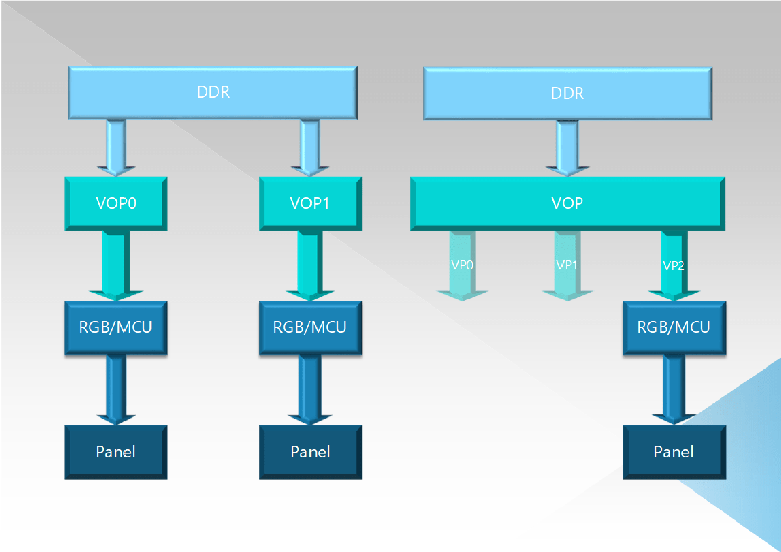
RGB/MCU paths for VOP 1.0/2.0
VOP (Video Output Process) is Rockchip’s display-processing unit. VOP 1.0 and VOP 2.0 differ mainly in multi-display support; see Rockchip_Developer_Guide_DRM_Display_Driver_CN. The left and right diagrams show RGB/MCU paths for VOP 1.0 and VOP 2.0 respectively. VOP reads and processes image data from DDR, then sends it to RGB/MCU. The interface converts the image into a protocol-compliant stream and transmits it to the panel.
4.2 Panel configuration
For the RGB panel driver, see drivers/gpu/drm/panel/panel-simple.c. A typical panel node is:
/ {
   panel: panel {

      compatible = "simple-panel";
      bus-format = <MEDIA_BUS_FMT_RGB888_1X24>;
      backlight = <&backlight>;
      enable-gpios = <&gpio3 RK_PA6 GPIO_ACTIVE_LOW>;
      enable-delay-ms = <20>;
      reset-gpios = <&gpio3 RK_PB0 GPIO_ACTIVE_LOW>;
      reset-delay-ms = <10>;
      status = "okay";

      display-timings {

         native-mode = <&fx070_dhm11boe_timing>;

         fx070_dhm11boe_timing: timing0 {
           clock-frequency = <50000000>;
           hactive = <1024>;
           vactive = <600>;
           hback-porch = <140>;
           hfront-porch = <160>;
           vback-porch = <20>;
           vfront-porch = <20>;
           hsync-len = <20>;
           vsync-len = <2>;

           hsync-active = <0>;
           vsync-active = <0>;
           de-active = <0>;
           pixelclk-active = <0>;
         };
      };

      port {
         panel_in_rgb: endpoint {
           remote-endpoint = <&rgb_out_panel>;
         };
      };
   };

};

&backlight {
   pwms = <&pwm9 0 25000 0>;
   status = "okay";
};
Set bus-format according to the panel’s display mode, usually determined from its datasheet pin definitions and driver-IC display-mode support. DTS macros are defined in include/uapi/linux/media-bus-format.h. Their hardware mappings are:
| Display mode | Bus format | Cycles per pixel |
|---|---|---|
| RGB888 (24bit) | MEDIA_BUS_FMT_RGB888_1X24 | 1 |
| RGB666 (18bit) | MEDIA_BUS_FMT_RGB666_1X18 | 1 |
| RGB666_CPADHI (18bit) | MEDIA_BUS_FMT_RGB666_1X24_CPADHI | 1 |
| RGB565 (16bit) | MEDIA_BUS_FMT_RGB565_1X16 | 1 |
| RGB565_CPADHI (16bit) | MEDIA_BUS_FMT_RGB565_1X24_CPADHI | 1 |
| RGB3x8 (8bit) | MEDIA_BUS_FMT_RGB888_3X8 MEDIA_BUS_FMT_RGB888_3X8 | 3 |
| RGB4x8(8bit) | MEDIA_BUS_FMT_RGB888_DUMMY_4X8 MEDIA_BUS_FMT_BGR888_DUMMY_4X8 | 4 |
Modify the backlight node’s pwms configuration to match the actual wiring. Ensure that the backlight is on before displaying an image. See Rockchip_Developer_Guide_Linux_PWM_CN.
Configure enable-gpios/reset-gpios and enable-delay-ms/reset-delay-ms/prepare-delay-ms/unprepare-delay-ms/disable-delay-ms according to panel power/reset timing requirements and the actual hardware circuit.
Optional: enable normally controls panel power. Its GPIO configuration depends on the power circuit.
Optional: the panel usually exposes a reset pin and describes reset conditions in its datasheet. GPIO configuration depends on the reset circuit.
Optional: configure enable-delay-ms/reset-delay-ms/prepare-delay-ms/unprepare-delay-ms/disable-delay-ms according to datasheet power/reset/signal timing.
The panel datasheet recommends display-timings values. They may be fine-tuned within the specified minimum/maximum limits for the application. The following datasheet corresponds to the example panel node:
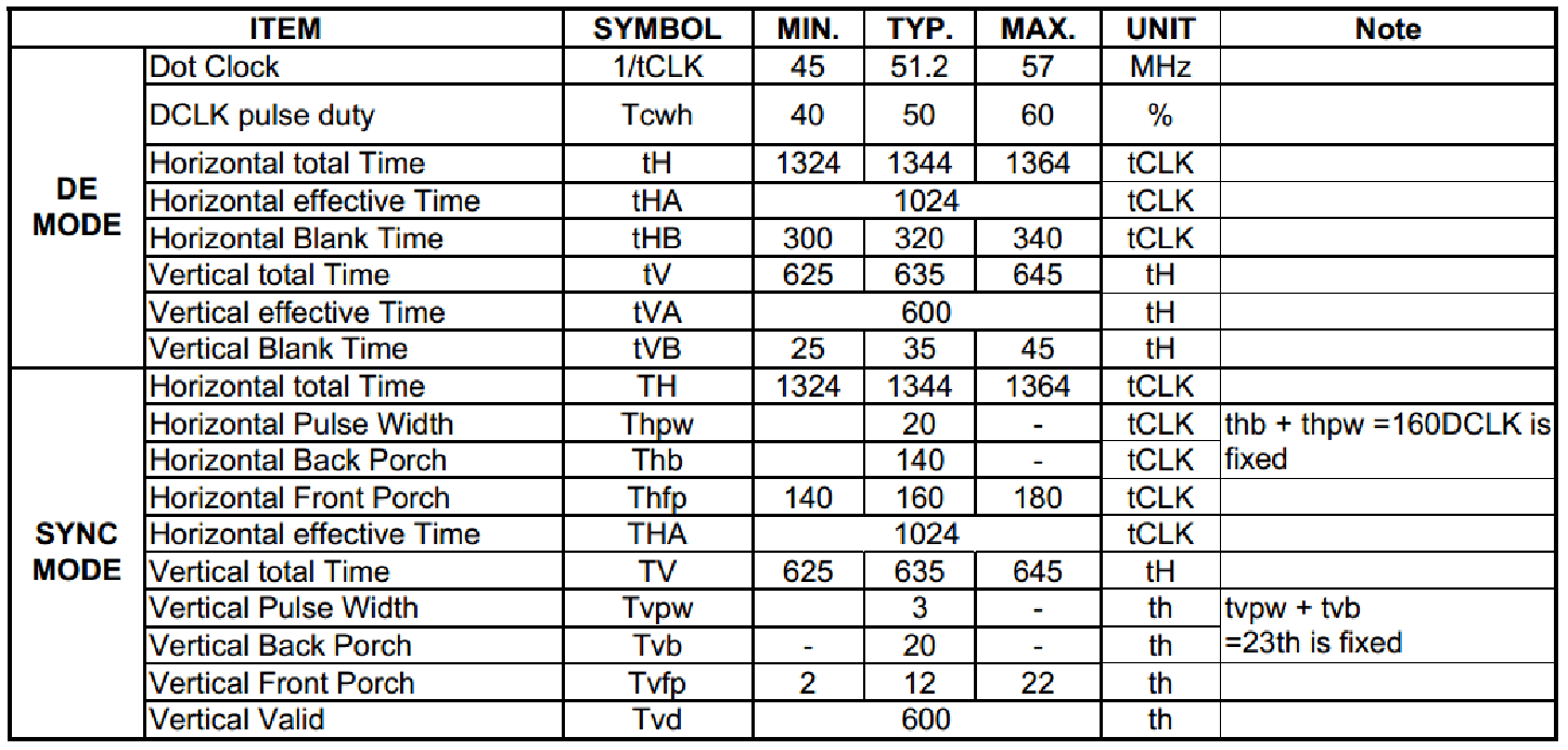
Original example panel timing table
| Mode | Parameter | Symbol | Min | Typ | Max | Unit | Note |
|---|---|---|---|---|---|---|---|
| DE | Dot clock | 1/tCLK | 45 | 51.2 | 57 | MHz | |
| DE | DCLK pulse duty | Tcwh | 40 | 50 | 60 | % | |
| DE | Horizontal total | tH | 1324 | 1344 | 1364 | tCLK | |
| DE | Horizontal effective | tHA | 1024 | tCLK | |||
| DE | Horizontal blank | tHB | 300 | 320 | 340 | tCLK | |
| DE | Vertical total | tV | 625 | 635 | 645 | tH | |
| DE | Vertical effective | tVA | 600 | tH | |||
| DE | Vertical blank | tVB | 25 | 35 | 45 | tH | |
| SYNC | Horizontal total | TH | 1324 | 1344 | 1364 | tCLK | |
| SYNC | Horizontal pulse width | Thpw | 20 | - | tCLK | thb + thpw = 160DCLK (fixed) | |
| SYNC | Horizontal back porch | Thb | 140 | - | tCLK | thb + thpw = 160DCLK (fixed) | |
| SYNC | Horizontal front porch | Thfp | 140 | 160 | 180 | tCLK | |
| SYNC | Horizontal effective | THA | 1024 | tCLK | |||
| SYNC | Vertical total | TV | 625 | 635 | 645 | th | |
| SYNC | Vertical pulse width | Tvpw | 3 | - | th | tvpw + tvb = 23th (fixed) | |
| SYNC | Vertical back porch | Tvb | - | 20 | - | th | tvpw + tvb = 23th (fixed) |
| SYNC | Vertical front porch | Tvfp | 2 | 12 | 22 | th | |
| SYNC | Vertical valid | Tvd | 600 | th |
DRM’s display_timing structure and member descriptions are in include/video/display_timing.h:
/*
 * Single "mode" entry. This describes one set of signal timings a display can
 * have in one setting. This struct can later be converted to struct videomode

 * (see include/video/videomode.h). As each timing_entry can be defined as a
 * range, one struct display_timing may become multiple struct videomodes.
 *
 * Example: hsync active high, vsync active low
 *
 *            Active Video
 * Video ______________________XXXXXXXXXXXXXXXXXXXXXX_____________________
 *  |<- sync ->|<- back ->|<----- active ----->|<- front ->|<- sync..
 *  |    |  porch |        |  porch |
 *
 * HSync _|¯¯¯¯¯¯¯¯¯¯|___________________________________________|¯¯¯¯¯¯¯¯¯
 *

 * VSync ¯|__________|¯¯¯¯¯¯¯¯¯¯¯¯¯¯¯¯¯¯¯¯¯¯¯¯¯¯¯¯¯¯¯¯¯¯¯¯¯¯¯¯¯¯¯|_________
 */
struct display_timing {
   struct timing_entry pixelclock;

   struct timing_entry hactive; /* hor. active video */
   struct timing_entry hfront_porch; /* hor. front porch */
   struct timing_entry hback_porch; /* hor. back porch */
   struct timing_entry hsync_len; /* hor. sync len */

   struct timing_entry vactive; /* ver. active video */
   struct timing_entry vfront_porch; /* ver. front porch */
   struct timing_entry vback_porch; /* ver. back porch */

   struct timing_entry vsync_len; /* ver. sync len */

   enum display_flags flags; /* display flags */
};
For RGB/MCU, clock-frequency in display-timings determines the VOP output frame rate. The calculation uses DRM timing properties htotal and vtotal. An excerpt follows; see include/drm/drm_modes.h for details.
The frame-rate calculation is implemented by drm_mode_vrefresh() in drivers/gpu/drm/drm_modes.c. With frame rate denoted by fr, the formula is:
fr = clock / (htotal * vtotal)
/**
 * struct drm_display_mode - DRM kernel-internal display mode structure

 * @hdisplay: horizontal display size
 * @hsync_start: horizontal sync start
 * @hsync_end: horizontal sync end
 * @htotal: horizontal total size
 * @hskew: horizontal skew?!
 * @vdisplay: vertical display size
 * @vsync_start: vertical sync start
 * @vsync_end: vertical sync end
 * @vtotal: vertical total size
 * @vscan: vertical scan?!
......
 *

 * The horizontal and vertical timings are defined per the following diagram.
 *
 * ::
 *
 *
 *          Active           Front      Sync       Back
 *         Region           Porch                  Porch
 *   <-----------------------><----------------><-------------><-------------->
 *    //////////////////////|
 *    ////////////////////// |
 *   ////////////////////// |.................. ................
 *                                  _______________

 *   <----- [hv]display ----->
 *   <------------- [hv]sync_start ------------>
 *   <--------------------- [hv]sync_end --------------------->
 *   <-------------------------------- [hv]total ----------------------------->*
 *
......
 */

/**
 * drm_mode_vrefresh - get the vrefresh of a mode
 * @mode: mode
 *
 * Returns:

 * @modes's vrefresh rate in Hz, rounded to the nearest integer. Calculates the
 * value first if it is not yet set.
 */
int drm_mode_vrefresh(const struct drm_display_mode *mode)
{
   unsigned int num, den;

   if (mode->htotal == 0 || mode->vtotal == 0)
      return 0;

   num = mode->clock;
   den = mode->htotal * mode->vtotal;


   if (mode->flags & DRM_MODE_FLAG_INTERLACE)
      num *= 2;
   if (mode->flags & DRM_MODE_FLAG_DBLSCAN)
      den *= 2;
   if (mode->vscan > 1)
      den *= mode->vscan;

   return DIV_ROUND_CLOSEST_ULL(mul_u32_u32(num, 1000), den);
}
EXPORT_SYMBOL(drm_mode_vrefresh);
4.2.1 SPI initialization
Some RGB panels require initialization commands over SPI. drivers/gpu/drm/panel/panel-simple.c supports the 3-wire 9-bit serial interface protocol:
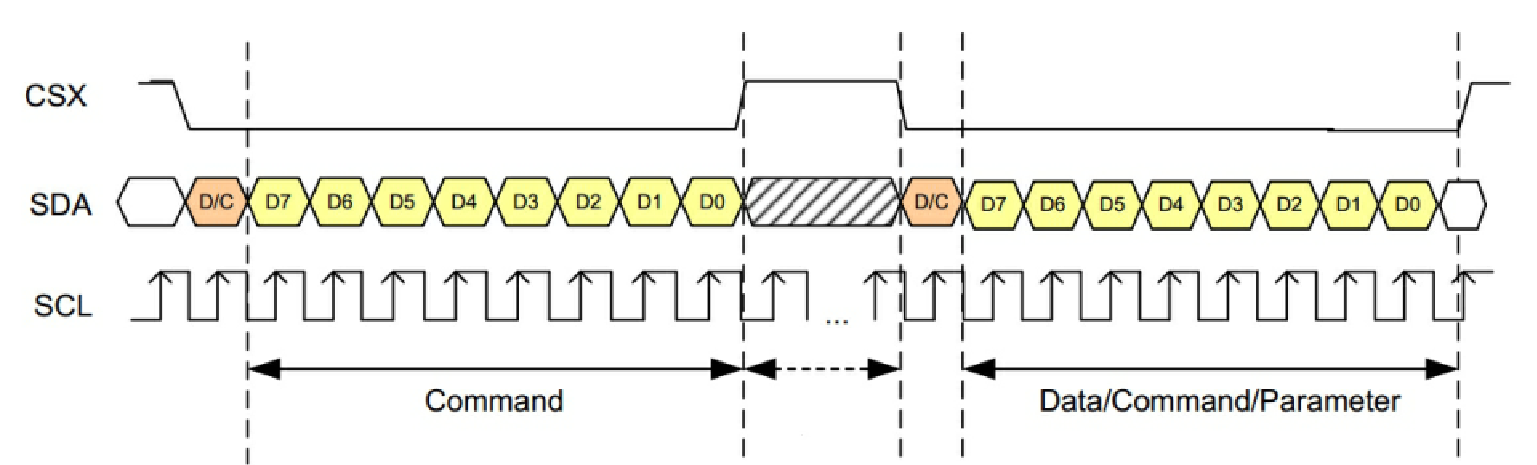
Three-wire 9-bit SPI initialization protocol
Rockchip SPI hardware supports transfer units of 4/8/16 bits, whereas this protocol uses 9 bits. Therefore panel-simple implements SPI through GPIO bit-banging.
Typical configuration for kernel-5.10 and later:
spi_gpio: spi-gpio {
   compatible = "spi-gpio";

   #address-cells = <0x1>;
   #size-cells = <0x0>;
   pinctrl-names = "default";
   pinctrl-0 = <&spi_gpio_pins>;
   spi-delay-us = <10>;
   status = "okay";

   sck-gpios = <&gpio4 RK_PA5 GPIO_ACTIVE_HIGH>;
   miso-gpios = <&gpio4 RK_PA7 GPIO_ACTIVE_HIGH>;
   mosi-gpios = <&gpio4 RK_PA6 GPIO_ACTIVE_HIGH>;
   cs-gpios = <&gpio4 RK_PA4 GPIO_ACTIVE_HIGH>;
   num-chipselects = <1>;


   /*
   * 320x480 RGB/MCU screen K350C4516T
   */
   panel: panel {
      compatible = "simple-panel-spi";
      reg = <0>;
      bus-format = <MEDIA_BUS_FMT_RGB666_1X18>;
      backlight = <&backlight>;
      enable-gpios = <&gpio3 RK_PA6 GPIO_ACTIVE_LOW>;
      enable-delay-ms = <20>;
      reset-gpios = <&gpio3 RK_PB0 GPIO_ACTIVE_LOW>;
      reset-delay-ms = <10>;

      prepare-delay-ms = <20>;
      unprepare-delay-ms = <20>;
      disable-delay-ms = <20>;
      init-delay-ms = <10>;
      width-mm = <217>;
      height-mm = <136>;
      rockchip,cmd-type = "spi";

      status = "okay";

      // type:0 is cmd, 1 is data
      panel-init-sequence = [
         /* type delay num val1 val2 val3 */
         00 00 01 e0
         01 00 01 00
         ......
         00 78 01 11
         00 00 01 29
      ];


      panel-exit-sequence = [
         //type delay num val1 val2 val3
         00 0a 01 28
         00 78 01 10
      ];

      display-timings {
         native-mode = <&kd050fwfba002_timing>;

         kd050fwfba002_timing: timing0 {
           /*
            * 10453500 for RGB666(18bit)
            */

           clock-frequency = <10453500>;
           hactive = <320>;
           vactive = <480>;
           hback-porch = <10>;
           hfront-porch = <5>;
           vback-porch = <10>;
           vfront-porch = <5>;
           hsync-len = <10>;
           vsync-len = <10>;
           hsync-active = <0>;
           vsync-active = <0>;
           de-active = <0>;

           pixelclk-active = <1>;
         };
      };

      port {
         panel_in_rgb: endpoint {
           remote-endpoint = <&rgb_out_panel>;
         };
      };
   };
};
Enable CONFIG_SPI_GPIO and configure sck-gpios, miso-gpios, mosi-gpios and
cs-gpios according to the hardware; see drivers/spi/spi-gpio.c. The panel node is essentially the same as above, with these points:
Change compatible to “simple-panel-spi”.
Set rockchip,cmd-type to “spi”.
Fill panel-init-sequence/panel-exit-sequence with the appropriate init/deinit sequences.
For kernel 4.19 and earlier, SPI RGB SDI/SCL/CS are emulated directly by GPIO in simple-panel without a third-party SPI driver. Note that SDI is not actually supported: the DTS property named SDI refers to hardware SDO, a typo in the early version. Example:
panel: panel {
   compatible = "simple-panel";

   ......
   spi-sdi-gpios = <&gpio1 RK_PC7 GPIO_ACTIVE_HIGH>;
   spi-scl-gpios = <&gpio1 RK_PD0 GPIO_ACTIVE_HIGH>;
   spi-cs-gpios = <&gpio1 RK_PD1 GPIO_ACTIVE_HIGH>;
   ......
   rockchip,cmd-type = "spi";

   /* type:0 is cmd, 1 is data */
   panel-init-sequence = [
      /* type delay num val1 val2 val3 */
       00  00 01 e0
       ......
       00  78 01 11

       00  00 01 29
   ];

   panel-exit-sequence = [
      /* type delay num val1 val2 val3 */
      00 0a 01 28
      00 78 01 10
   ];
   ......
};
Reference SPI RGB configurations by kernel version:
kernel 4.19 and earlier: arch/arm64/boot/dts/rockchip/rk3308-evb-ext-v10.dtsi
kernel 5.10 and later: arch/arm64/boot/dts/rockchip/rk3562-evb1-lp4x-v10-rgb-k350c4516t.dts
4.3 RGB interface
The RGB driver is drivers/gpu/drm/rockchip/rockchip_rgb.c. Reference DTS configuration:
&rgb {
   status = "okay";

   pinctrl-0 = <&rgb666_pins>;
   ports {
      port@1 {
         reg = <1>;


         rgb_out_panel: endpoint {
           remote-endpoint = <&panel_in_rgb>;
         };
      };
   };
};

//VOP 1.0
&rgb_in_vop {
   status = "okay";
};


//VOP 2.0
&rgb_in_vp0 {
   status = "okay";
};
RGB node configuration differs between VOP 1.0 and VOP 2.0. Reference configurations:
VOP 1.0: arch/arm/boot/dts/rv1106-evb-ext-rgb-v10.dtsi.
VOP 2.0: arch/arm64/boot/dts/rockchip/rk3562-evb1-lp4x-v10-rgb-FX070-DHM11BOE-A.dts.
Choose pinctrl according to actual hardware connections. Pin-order definitions are in rkxxxx-pinctrl.dtsi/rvxxxx-pinctrl.dtsi.
4.4 MCU interface
The MCU interface and MCU panel drivers are in drivers/gpu/drm/rockchip/rockchip_rgb.c. DTS is essentially the same as for RGB, with additional MCU-mode selection and timing. Reference configuration:
&rgb {
   status = "okay";

   rockchip,data-sync-bypass;
   pinctrl-names = "default";
   /*
   * rgb3x8_pins_m0/rgb3x8_pins_m1 for RGB3x8(8bit)
   * rgb565_pins for RGB565(16bit)
   */
   pinctrl-0 = <&rgb565_pins>;

   /*
   * 320x480 RGB/MCU screen K350C4516T
   */
   mcu_panel: mcu-panel {
      /*

      * MEDIA_BUS_FMT_RGB888_3X8 for RGB3x8(8bit)
       * MEDIA_BUS_FMT_RGB565_1X16 for RGB565(16bit)
       */
      bus-format = <MEDIA_BUS_FMT_RGB565_1X16>;

      backlight = <&backlight>;
      enable-gpios = <&gpio1 RK_PA3 GPIO_ACTIVE_LOW>;
      enable-delay-ms = <20>;
      reset-gpios = <&gpio1 RK_PA4 GPIO_ACTIVE_LOW>;
      reset-value = <0>;
      reset-delay-ms = <10>;
      prepare-delay-ms = <20>;
      unprepare-delay-ms = <20>;
      disable-delay-ms = <20>;
      init-delay-ms = <10>;
      width-mm = <217>;
      height-mm = <136>;


      // type:0 is cmd, 1 is data
      panel-init-sequence = [
         //type delay num val1 val2 val3
          ......
          01  00 01 55 /*
                       * interface pixel format:
                       * 66 for RGB3x8(8bit)
                       * 55 for RGB565(16bit)
                       */
          ......
          01  00 01 a0 /*
                       * frame rate control:

                       * 70 (45hz) for RGB3x8(8bit)
                       * a0 (60hz) for RGB565(16bit)
                       */
          ......
          01  00 01 02 /*
                       * display function control:
                       * 32 for RGB
                       * 02 for MCU
                       */
          00  78 01 11
          00  32 01 29
          00  00 01 2c

      ];

      panel-exit-sequence = [
         //type delay num val1 val2 val3
          00  0a 01 28
          00  78 01 10
      ];

      display-timings {
         native-mode = <&kd050fwfba002_timing>;

         kd050fwfba002_timing: timing0 {
            /*
             * 7840125 for frame rate 45Hz
             * 10453500 for frame rate 60Hz
             */

            clock-frequency = <10453500>;
            hactive = <320>;
            vactive = <480>;
            hback-porch = <10>;
            hfront-porch = <5>;
            vback-porch = <10>;
            vfront-porch = <5>;
            hsync-len = <10>;
            vsync-len = <10>;
            hsync-active = <0>;
            vsync-active = <0>;
            de-active = <0>;

            pixelclk-active = <1>;
         };
      };

      port {
            panel_in_rgb: endpoint {
               remote-endpoint = <&rgb_out_panel>;
            };
         };
      };

      ports {
         rgb_out: port@1 {

            reg = <1>;
            #address-cells = <1>;
            #size-cells = <0>;

            rgb_out_panel: endpoint@0 {
               reg = <0>;
               remote-endpoint = <&panel_in_rgb>;
            };
         };
      };
   };
};


//VOP 1.0
&rgb_in_vop {
   status = "okay";
};

&vop {
   status = "okay";

   /*
    * Default config is as follows:
    *
    * mcu-pix-total = <9>;
   * mcu-cs-pst = <1>;
   * mcu-cs-pend = <8>;
   * mcu-rw-pst = <2>;

   * mcu-rw-pend = <5>;
   * mcu-hold-mode = <0>; // default set to 0
   *
   * To increase the frame rate, reduce all parameters because
   * the max dclk rate of mcu is 150M in rv1103/rv1106.
   */
   mcu-timing {
      mcu-pix-total = <5>;
      mcu-cs-pst = <1>;
      mcu-cs-pend = <4>;
      mcu-rw-pst = <2>;
      mcu-rw-pend = <3>;


      mcu-hold-mode = <0>; // default set to 0
   };
};

//VOP 2.0
&rgb_in_vp0 {
   status = "okay";
};

&vp0 {
   status = "okay";


   /*
   * Default config is as follows:
   *
   * mcu-pix-total = <9>;
   * mcu-cs-pst = <1>;
   * mcu-cs-pend = <8>;
   * mcu-rw-pst = <2>;
   * mcu-rw-pend = <5>;
   * mcu-hold-mode = <0>; // default set to 0
   *
   * To increase the frame rate, reduce all parameters because
   * the max dclk rate of mcu is 150M in rk3562.

   */
   mcu-timing {
      mcu-pix-total = <5>;
      mcu-cs-pst = <1>;
      mcu-cs-pend = <4>;
      mcu-rw-pst = <2>;
      mcu-rw-pend = <3>;

      mcu-hold-mode = <0>; // default set to 0
   };
};
MCU node configuration differs between VOP 1.0 and VOP 2.0. Reference configurations:
VOP 1.0: arch/arm/boot/dts/rv1106-evb-ext-mcu-v10.dtsi.
VOP 2.0: arch/arm64/boot/dts/rockchip/rk3562-evb1-lp4x-v10-mcu-k350c4516t.dts. The driver selects MCU or RGB using rockchip,data-sync-bypass under the rgb node. Without the property, RGB is the default; enabling it selects MCU.
For kernel-5.10 and later, place the MCU panel under the rgb node. For kernel-4.19 and earlier, initialize it through simple-panel as an independent node. When moving a panel node from simple-panel under rgb, note:
Name the node mcu-panel; the driver uses this name to identify and parse MCU panel parameters.
The compatible property may be removed; it is not required.
An MCU panel usually needs an initialization sequence for display mode, pixel format and frame rate (depending on its driver IC), and a deinitialization sequence to turn it off or enter low-power mode. For panel-init-sequence and panel-exit-sequence:
The panel manufacturer supplies the sequence, which usually must be converted from a C file into DTS.
Each sequence row contains, from left to right: command type cmd/data, delay in ms, data length in bytes, and data.
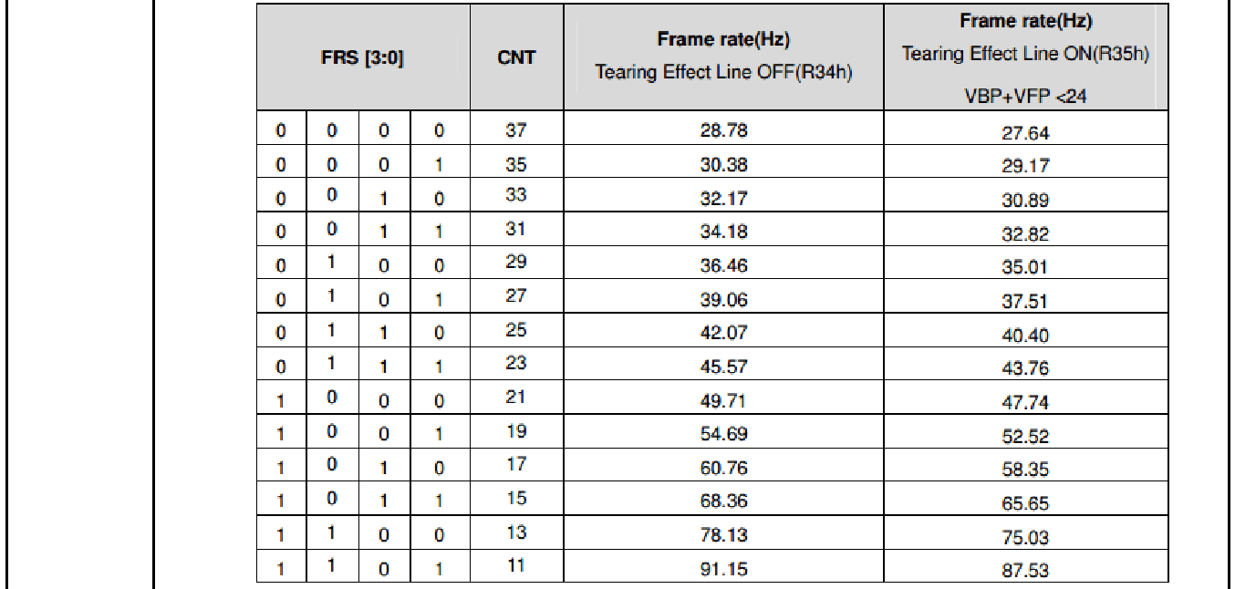
Frame rate is normally configured during sequence initialization and must match the rate calculated in Panel Configuration. The example driver-IC manual states:
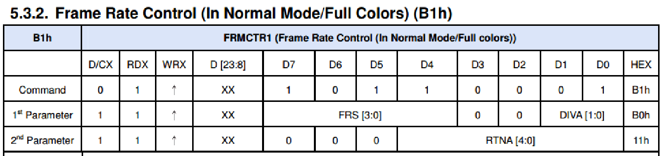
Original FRMCTR1 frame-rate-control register table
| FRMCTR1 (B1h) | D/CX | RDX | WRX | D[23:8] | D7..D0 | HEX |
|---|---|---|---|---|---|---|
| Command | 0 | 1 | ↑ | XX | 1 0 1 1 0 0 0 1 | B1h |
| 1st parameter | 1 | 1 | ↑ | XX | FRS[3:0] / 0 / 0 / DIVA[1:0] | B0h |
| 2nd parameter | 1 | 1 | ↑ | XX | 0 / 0 / 0 / RTNA[4:0] | 11h |
Original excerpt of FRS/frame-rate mapping
| FRS[3:0] | CNT | Hz / TE OFF (R34h) | Hz / TE ON (R35h), VBP+VFP <24 |
|---|---|---|---|
| 0000 | 37 | 28.78 | 27.64 |
| 0001 | 35 | 30.38 | 29.17 |
| 0010 | 33 | 32.17 | 30.89 |
| 0011 | 31 | 34.18 | 32.82 |
| 0100 | 29 | 36.46 | 35.01 |
| 0101 | 27 | 39.06 | 37.51 |
| 0110 | 25 | 42.07 | 40.40 |
| 0111 | 23 | 45.57 | 43.76 |
| 1000 | 21 | 49.71 | 47.74 |
| 1001 | 19 | 54.69 | 52.52 |
| 1010 | 17 | 60.76 | 58.35 |
| 1011 | 15 | 68.36 | 65.65 |
| 1100 | 13 | 78.13 | 75.03 |
| 1101 | 11 | 91.15 | 87.53 |
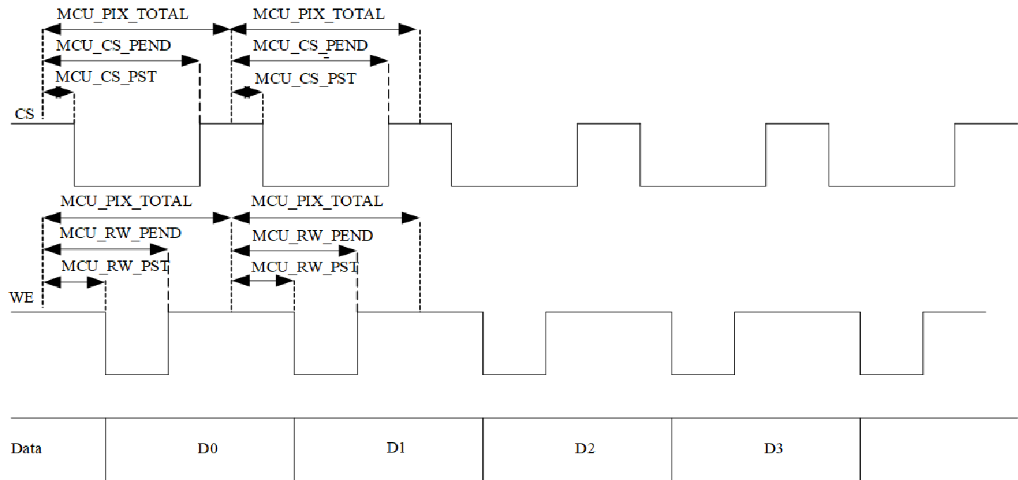
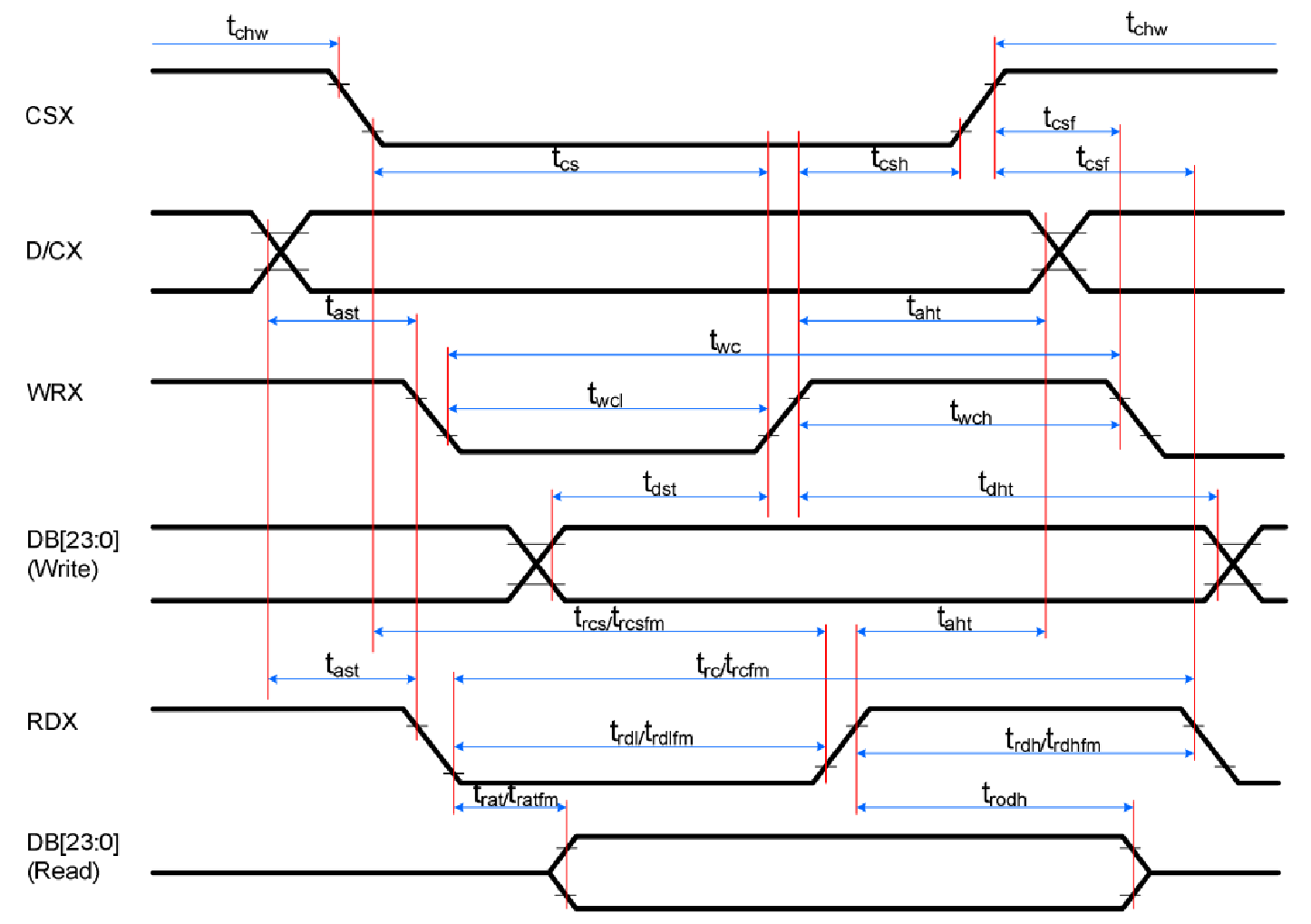
mcu-timing configures normal-mode control signals CSN/WEN/REN. Its properties correspond to the intervals below. Detailed timing and interval requirements are from the datasheet of the panel used in the DTS example. The following explains how to configure mcu-timing and clock-frequency in display-timings.
MCU normal-mode control-signal timing
Panel write/read timing
Original panel driver-IC timing requirements
| Signal | Symbol | Parameter | Min | Max | Unit | Description |
|---|---|---|---|---|---|---|
| DCX | tast | Address setup time | 0 | - | ns | - |
| DCX | that | Address hold time (write/read) | 0 | - | ns | - |
| CSX | tchw | CSX high pulse width | 0 | - | ns | - |
| CSX | tcs | Chip select setup (write) | 15 | - | ns | - |
| CSX | trcs | Chip select setup (read ID) | 45 | - | ns | - |
| CSX | trcsfm | Chip select setup (read FM) | 355 | - | ns | - |
| CSX | tcsf | Chip select wait (write/read) | 0 | - | ns | - |
| WRX | twc | Write cycle | 30 | - | ns | - |
| WRX | twrh | Write control high duration | 15 | - | ns | - |
| WRX | twrl | Write control low duration | 15 | - | ns | - |
| RDX (FM) | trcfm | Read cycle (FM) | 450 | - | ns | Read frame memory |
| RDX (FM) | trdhfm | Read control high duration (FM) | 90 | - | ns | Read frame memory |
| RDX (FM) | trdlfm | Read control low duration (FM) | 355 | - | ns | Read frame memory |
| RDX (ID) | trc | Read cycle (ID) | 160 | - | ns | Read ID data |
| RDX (ID) | trdh | Read control high duration | 90 | - | ns | Read ID data |
| RDX (ID) | trdl | Read control low duration | 45 | - | ns | Read ID data |
| DB[23:0], DB[17:0], DB[15:0], DB[8:0], DB[7:0] | tdst | Write data setup | 10 | - | ns | Maximum: CL=30pF; minimum: CL=8pF |
| DB[23:0], DB[17:0], DB[15:0], DB[8:0], DB[7:0] | tdht | Write data hold | 10 | - | ns | Maximum: CL=30pF; minimum: CL=8pF |
| DB[23:0], DB[17:0], DB[15:0], DB[8:0], DB[7:0] | trat | Read access | - | 40 | ns | Maximum: CL=30pF; minimum: CL=8pF |
| DB[23:0], DB[17:0], DB[15:0], DB[8:0], DB[7:0] | tratfm | Read access | - | 340 | ns | Maximum: CL=30pF; minimum: CL=8pF |
| DB[23:0], DB[17:0], DB[15:0], DB[8:0], DB[7:0] | trod | Read output disable | 20 | 80 | ns | Maximum: CL=30pF; minimum: CL=8pF |
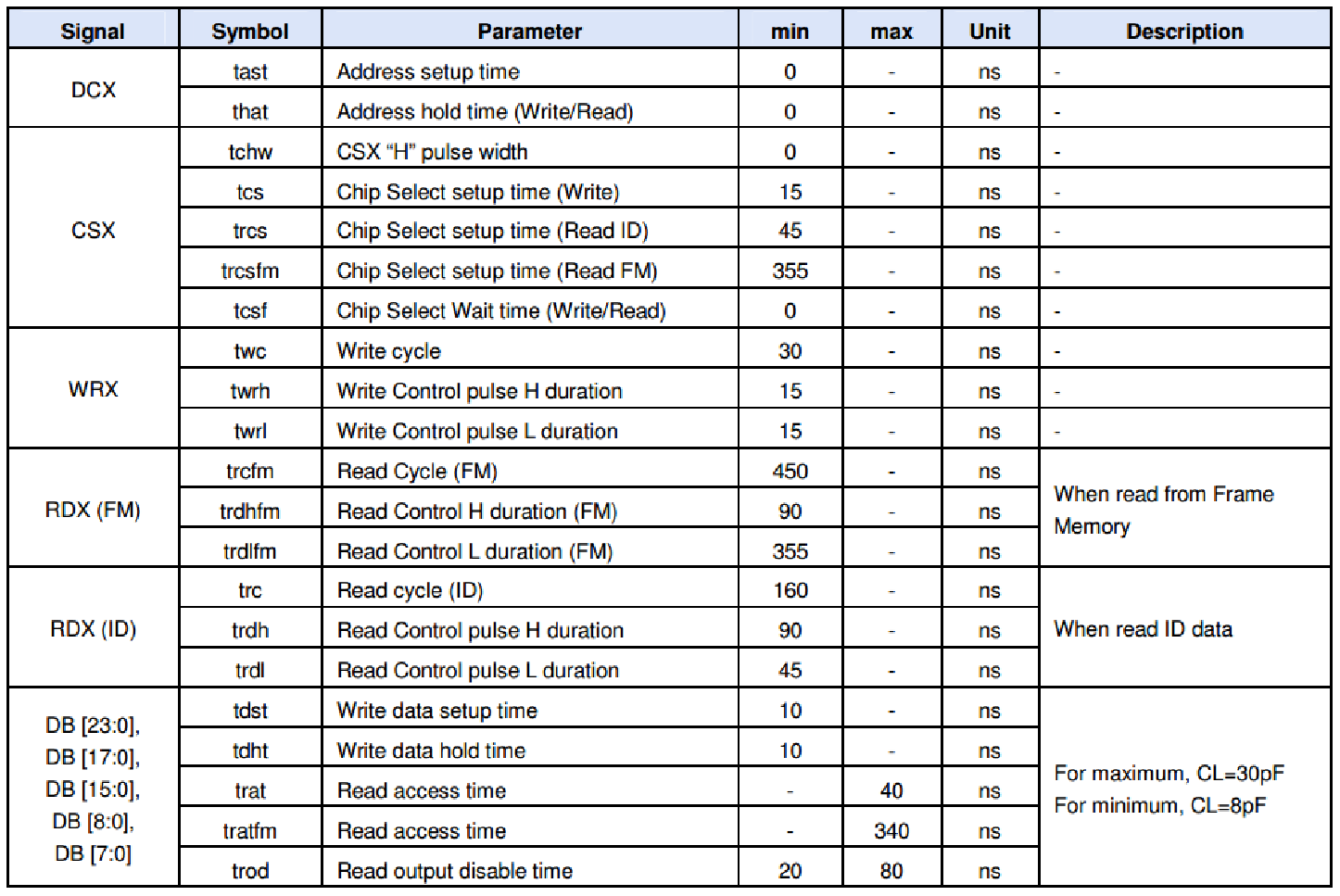
Let ptotal be mcu-pix-total in mcu-timing. The panel datasheet requires the MCU_PIX_TOTAL interval to be no shorter than tmin:
The panel datasheet gives twc = 40, while the driver-IC datasheet gives twc = 30; use the larger value.
tmin = T_CHW + T_AST + T_WC + T_CHW = 40 ns
The example panel supports MEDIA_BUS_FMT_RGB888_3X8 and MEDIA_BUS_FMT_RGB565_1X16. Let cpp denote Cycles Per Pixel, the number of cycles used to transmit one pixel (see Panel Configuration). Their theoretical maximum frame rates, frs-max and frp-max, are:
fr < 1000000000 / (htotal * ptotal * cpp * tmin)
htotal = hactive + hback-porch + hfront-porch + hsync-len = 345
vtotal = vactive + vback-porch + vfront-porch + vsync-len = 505
fr_s-max < 1000000000 / (345 * 505 * 3 * 40) ≈ 47.83 Hz
fr_p-max < 1000000000 / (345 * 505 * 1 * 40) ≈ 143.49 Hz
Editorial note: the general source formula uses ptotal, but the numerical substitution uses 505 (the stated vtotal). Both are retained without silently correcting the formula.
The source therefore selects frs = 45(Hz) for serial rgb3x8 and frp = 60(Hz) for parallel rgb1x16.
Below, suffix s means serial and suffix p means parallel.
The clock-frequency values in display-timings are:
clock_s = fr_s * htotal * vtotal = 45 * 345 * 505 = 7840125
clock_p = fr_p * htotal * vtotal = 60 * 345 * 505 = 10453500
Each platform limits MCU dclk. See mcu_max_dclk_rate in drivers/gpu/drm/rockchip/rockchip_rgb.c; it is normally 150000000 Hz. The check is implemented in rockchip_rgb_encoder_mode_valid().
Using dclkmax and the frame rate fr configured in the initialization sequence (normally 60Hz), calculate the maximum ptotal:
ptotal_max < dclk_max / (cpp * clock) - 1
ptotal_s-max < 150000000 / (3 * 7840125) - 1 ≈ 5.38
ptotal_p-max < 150000000 / (1 * 10453500) - 1 ≈ 13.35
Choose the smaller value, ptotal = 5, and determine the remaining mcu-timing values from the timing diagram.
Finally validate the calculated actual values against the datasheet timing requirements.
Actual MCU dclk is not simply clock-frequency from display-timings; it also depends on mcu-pix-total in mcu-timing and Cycles Per Pixel:
dclk = clock * cpp * (ptotal + 1)
dclk_s = 7840125 * 3 * 6 = 141122250
dclk_p = 10453500 * 1 * 6 = 62721000
Both dclk values remain below dclkmax. The actual MCU_PIX_TOTAL durations are:
t_s = (ptotal + 1) * 1000000000 / dclk_s ≈ 42.52 ns
t_p = (ptotal + 1) * 1000000000 / dclk_p ≈ 95.66 ns
Both MCU_PIX_TOTAL durations t satisfy the requirement to exceed 40 ns.
4.4.1 MCU bypass timing
Early MCU-capable platforms such as RK3308 and PX30 use the same timing for bypass and normal modes. Starting with RK3562, the IC design was optimized and the driver provides default bypass timing for most write/read needs. See vop_mcu_bypass_cfg definitions in drivers/gpu/drm/rockchip/rockchip_vop_reg.c and drivers/gpu/drm/rockchip/rockchip_vop2_reg.c, for example:
static struct rockchip_mcu_timing rk3506_mcu_bypass_timing = {
   .mcu_pix_total = 26,
   .mcu_cs_pst = 3,

   .mcu_cs_pend = 24,
   .mcu_rw_pst = 6,
   .mcu_rw_pend = 15,
};

static const struct vop_mcu_bypass_cfg rk3506_mcu_bypass_cfg = {
   .timing = &rk3506_mcu_bypass_timing,
   .dclk_rate = 120000000,
};
If the default bypass timing does not meet the application requirements, specify it in DTS; see arch/arm/boot/dts/rk3506g-evb1-v10-mcu-k350c4516t.dts:
&vop {
   mcu-timing {

      mcu-pix-total = <5>;
      mcu-cs-pst = <1>;
      mcu-cs-pend = <4>;
      mcu-rw-pst = <2>;
      mcu-rw-pend = <3>;

      mcu-hold-mode = <0>;
   };

   mcu-bypass-timing {
      mcu-pix-total = <9>;
      mcu-cs-pst = <1>;
      mcu-cs-pend = <8>;

      mcu-rw-pst = <2>;
      mcu-rw-pend = <7>;

      mcu-hold-mode = <0>;
   };
};
Bypass mode can include MCU reads. Minimum read-timing limits are normally larger than write-timing limits (see the previous example datasheet), so mcu-bypass-timing is usually calculated from read limits to satisfy both write and read requirements.
4.4.2 MCU frame write/read
In MCU normal mode, frame write/read allows commands to be exchanged between host and panel between frames, for example reading status registers or changing the display start position. It is commonly used in electrostatic stress tests or for panels requiring a per-frame display-start update.
Enable the feature by configuring panel-frame-sequence in DTS. See arch/arm/boot/dts/rk3506g-evb1-v10-mcu-k350c4516t.dts:
&rgb {
   ......
   mcu_panel: mcu-panel {

      ......
      panel-frame-sequence = [
         //type delay num val1 val2 val3
          00  00 01 0a
          02  00 01 0a
          02  00 01 0a
          00  00 01 2c
      ];
      ......
   };
   ......
};
Inter-frame write/read is implemented in drivers/gpu/drm/rockchip/rockchip_rgb.c:
static void mcu_interframe_work_func(struct work_struct *work)
{
   struct rockchip_mcu_panel *mcu_panel =

      container_of(work, struct rockchip_mcu_panel, interframe_work);
   struct drm_panel *panel = &mcu_panel->base;
   struct drm_display_mode *mode = mcu_panel->desc->mode;
   struct drm_crtc *crtc = mcu_panel->encoder->crtc;
   u32 timeout = DIV_ROUND_CLOSEST_ULL(1000, drm_mode_vrefresh(mode));
   int ret;

   ret = rockchip_drm_wait_vact_end(crtc, timeout);
   if (ret) {
      DRM_DEV_ERROR(panel->dev, "wairt vact end timed out\n");
      return;
   }


   ret = rockchip_mcu_panel_xfer_mcu_cmd_seq(mcu_panel, mcu_panel->desc->frame_seq);
   if (ret) {
      DRM_DEV_ERROR(panel->dev, "failed to send frame cmds seq\n");
      return;
   }

   schedule_work(&mcu_panel->interframe_work);
};
For specific application requirements, modify the implementation of the work item above.
5. Debugging procedure
1. Verify the hardware connections of every RGB/MCU pin. Pin mappings can differ between platforms; see
Hardware Connections above.
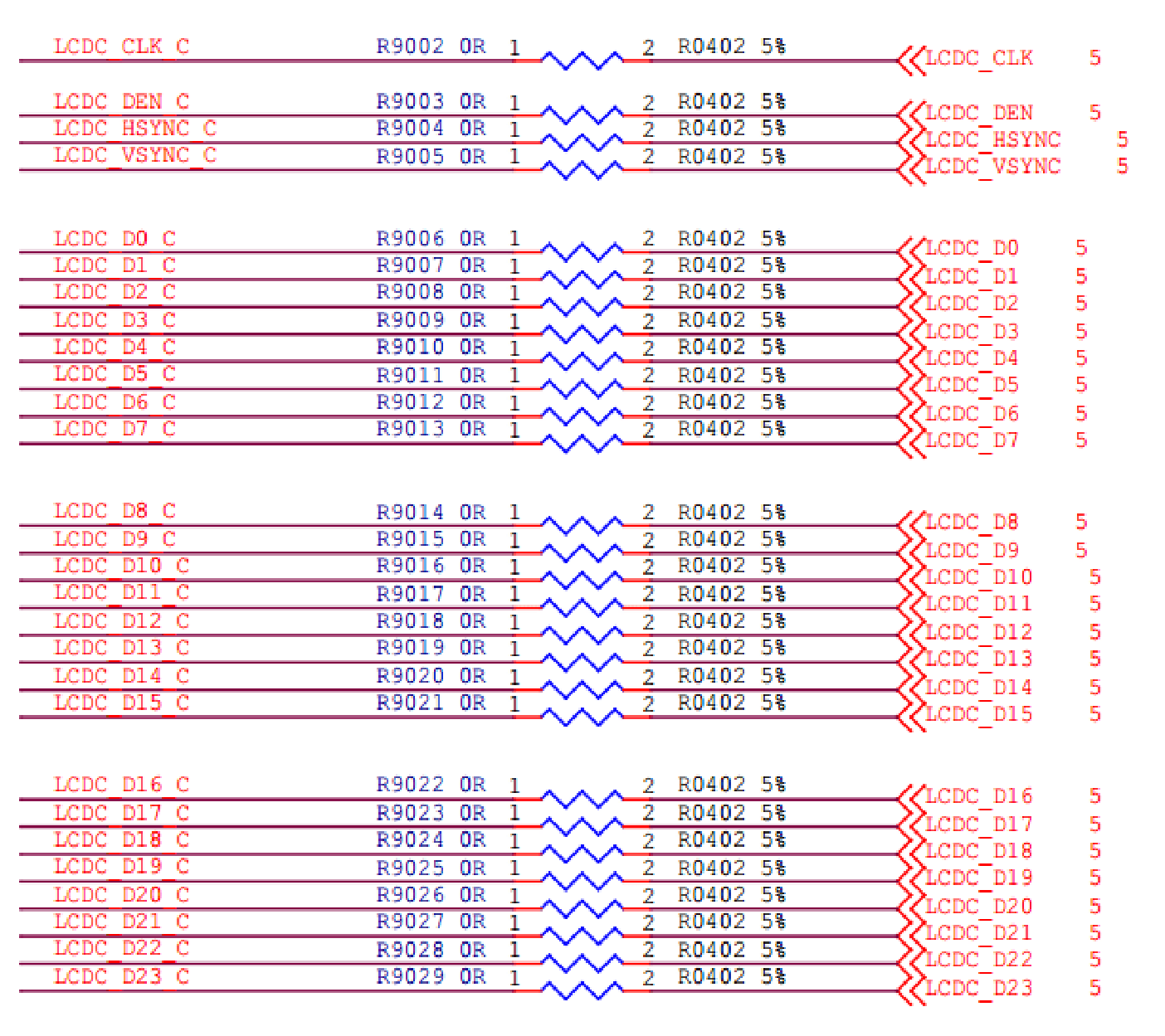
Example RGB/MCU pin connections
2. Use the panel datasheet to configure enable/reset polarity, power sequencing and the backlight PWM channel. For MCU panels, also configure the correct initialization sequence.

Example reset, enable and backlight PWM connections
3. With the backlight on, verify the enable/reset levels again. If measurements are still unexpected, verify that iomux selects GPIO correctly.
6. Common issues
6.1 RGB/MCU displays an image with noise or misalignment
Try inverting dclk polarity using pixelclk-active under display-timings. This changes the relative phase of dclk and data.
display-timings {
   native-mode = <&fx070_dhm11boe_timing>;


   fx070_dhm11boe_timing: timing0 {
      clock-frequency = <50000000>;
      hactive = <1024>;
      vactive = <600>;
      hback-porch = <140>;
      hfront-porch = <160>;
      vback-porch = <20>;
      vfront-porch = <20>;
      hsync-len = <20>;
      vsync-len = <2>;
      hsync-active = <0>;
      vsync-active = <0>;

      de-active = <0>;
      pixelclk-active = <0>; // 1 翻转,0 不翻转
   };
};