
本文为 Rockchip RGB/MCU 平台参考,原文 V1.7.1 的支持表列出 RK1808、RK312X/PX3SE、RK3288、RK3308B/BS、RK3326/PX30、RK3506、RK3562、RK3568、RK3576、RV1103/1106、RV1109/RV1126 和 RV1126B;各平台能力不同,不能据此宣称所有 ArmSoM 板卡支持。SPI/Panel 配置按原文区分 kernel 4.19 及以下与 5.10 及以上;实际 SDK/BSP、接口引出、引脚复用、电压、Panel 时序仍须按板卡确认。未进行 ArmSoM 硬件验证,原文日志/数值/截图仅作平台示例。
来源:Rockchip_Developer_Guide_RGB_MCU_CN.pdf,V1.7.1,34 页。只提供中文稿;英文/俄文完整翻译中文技术正文,三语均使用中文 PDF 的原图,图内文字不伪称已翻译。
校对记录 · ArmSoM documentation · Rockchip
1. 基础概念
1.1 RGB 接口
RGB 接口也被称为 DPI(Display Pixel Interface) 接口,RGB 接口用于同步的信号有 Vsync、Hsync、Den(Enable)和 DCLK(Dotclk)四个引脚,根据同步方式的不同可以分为 DE mode 和 SYNC mode,Rockchip 平台RGB 接口的输出时序可以同时兼容两者。
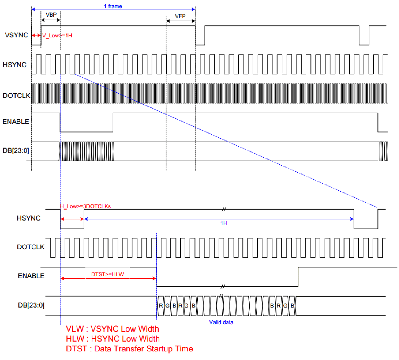
DE 模式时序
1.1.1 DE Mode
DB[23:0] 数据是否有效仅由 Den 信号决定,低电平时数据有效,反之无效。
1.1.2 SYNC Mode
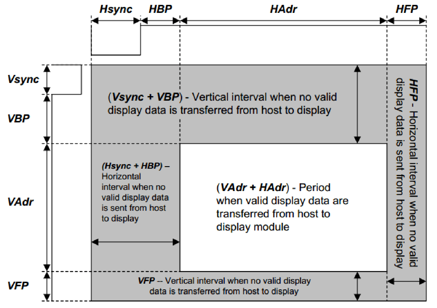
SYNC 模式时序
DB[23:0] 数据由 Vsync 和 Hsync 信号来同步,按照上图时序扫描数据。
1.2 MCU 接口
MCU 接口也被称为 DBI 接口或 8080 接口,支持 TX 和 RX 端的双向通信,有 RS(CSX)、CSN(D/CX)、WEN(WRX)和 REN(RDX)四个同步信号,RK 平台仅支持 MCU 接口的 TX 功能。
1.2.1 Write Timing
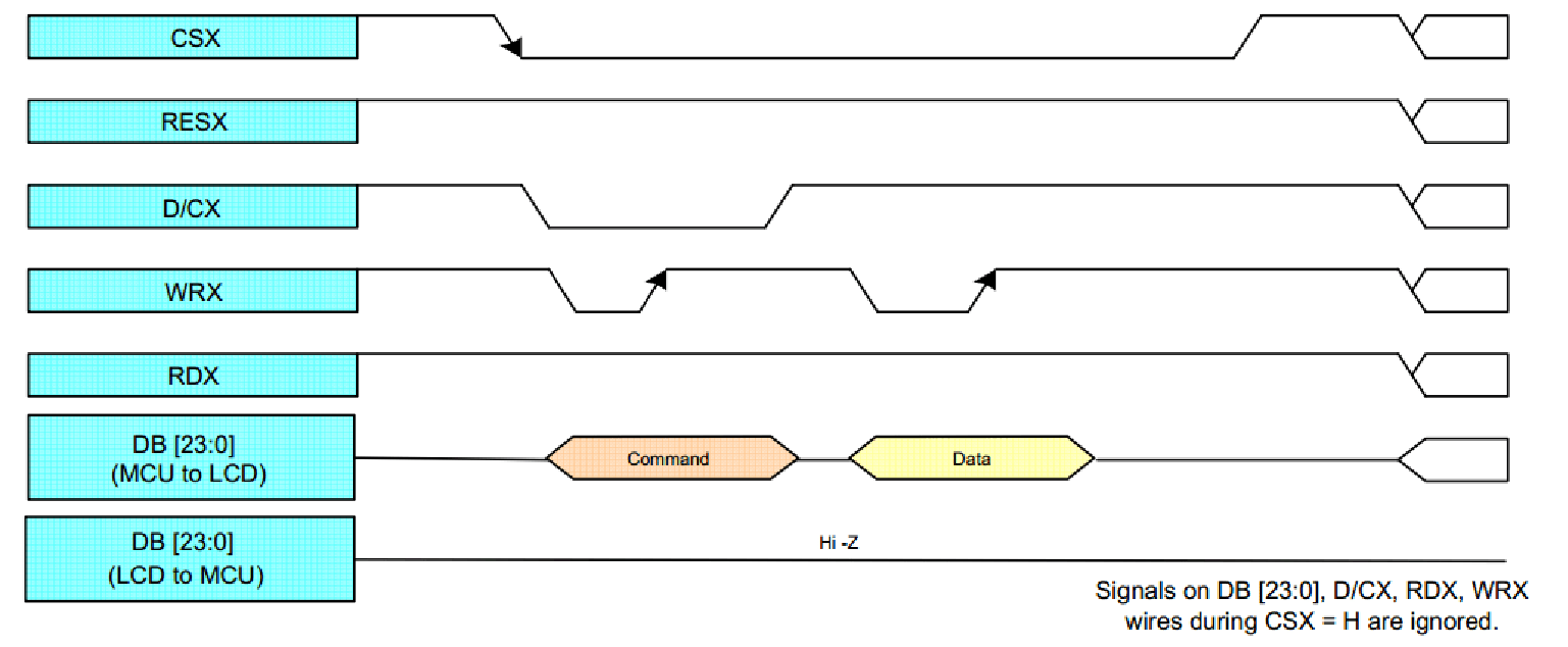
MCU 写时序
CSX、D/CX 和 WRX 引脚依次拉低,在 DB[23:0] 数据有效期间 WRX 信号会先拉低再拉高。
1.2.2 Read Timing
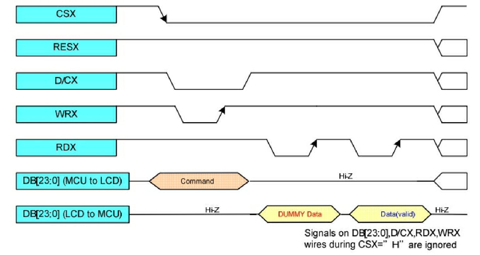
MCU 读时序及首个无效数据
CSX、D/CX 和 RDX 引脚依次拉低,在 DB[23:0] 数据有效期间 RDX 信号会先拉低再拉高。
read 前先通过一次 write 将所读取的寄存器地址传输给 Panel 端。
第一次 read 返回的数据是无效的,从第二次 read 开始才是有效的数据。
MCU read 通常用于 panel 调试期间 debug、通过区分 panel ID 实现多屏兼容功能等应用场景,以及会在下文中介绍的 frame read 功能。
1.2.3 Bypass 和 Normal Mode
bypass 模式:当 MCU 和 panel 之间通过 write/read 操作进行指令传输时,工作于 bypass 模式。
MCU 接口根据 panel-init-sequence/panel-exit-sequence 传输 init/deinit 指令,以及进行 frame write/read时(详⻅后文《软件配置》章节中的相关说明),均属于 bypass 模式。
normal 模式:主控将图像通过 MCU 接口传输到 panel 端的 ram 中并正常显示的模式,通常在传输完 panel-init-sequence 并确认 panel 正常初始化后就会进入到该模式。
bypass 模式下可以包含 write/read 操作,normal 模式下仅为 write 操作。
2. RK 平台支持情况
| SOC 平台 | 是否支 持 RGB | 是否支持 MCU | 是否支持 MCU Read | VOP Version | Video Port 通路 (for VOP 2.0) | Output Mode 支持 |
|---|---|---|---|---|---|---|
| RK1808 | Y | Y | N | VOP 1.0 | RGB666/RGB565 | |
| RK312X/PX3SE | Y | N | N | VOP 1.0 | RGB888/RGB666/RGB565 | |
| RK3288 | Y | Y | N | VOP 1.0 | RGB888/RGB666/RGB565/RGB3x8 | |
| RK3308B/RK3308BS | Y | Y | N | VOP 1.0 | RGB888/RGB666/RGB565/RGB3x8 | |
| RK3326/PX30 | Y | Y | N | VOP 1.0 | RGB888/RGB666/RGB565 | |
| RK3506 | Y | Y | Y | VOP 1.0 | RGB888/RGB666/RGB565/RGB3x8/RGB3x6/RGB2x8 | |
| RK3562 | Y | Y | N | VOP 2.0 | VP0 | RGB888/RGB666/RGB565/RGB3x8 |
| RK3568 | Y | N | N | VOP 2.0 | VP2 | RGB888/RGB666/RGB565 |
| RK3576 | Y | Y | N | VOP 2.0 | VP1/VP2 | RGB888/RGB666/RGB565/RGB3x8/RGB3x6/RGB2x8 |
| RV1103 | Y | Y | N | VOP 1.0 | RGB3x8 | |
| RV1106 | Y | Y | N | VOP 1.0 | RGB666/RGB565/RGB3x8 | |
| RV1109/RV1126 | Y | Y | N | VOP 1.0 | RGB888/RGB666/RGB565/RGB3x8 | |
| RV1126B | Y | Y | Y | VOP 1.0 | RGB888/RGB666/RGB565/RGB3x8/RGB3x6/RGB2x8 |
注:上述 VOP 及 VP(Video Port)相关概念参考文档《Rockchip_Developer_Guide_DRM_Display_Driver_CN》。
3. 硬件连接
3.1 RK3562/RK3576/RK3506/RV1126B 平台
| Component Name | Pin Name | RGB888 (MCU) | RGB666 (MCU) | RGB565 (MCU) | RGB3x8 (MCU) | RGB3x6 (MCU) | RGB2x8 (MCU) |
|---|---|---|---|---|---|---|---|
| DCLK | VO_LCDC_CLK | DCLK(RS) | DCLK(RS) | DCLK(RS) | DCLK(RS) | DCLK(RS) | DCLK(RS) |
| VSYNC | VO_LCDC_VSYNC | VSYNC(CSN) | VSYNC(CSN) | VSYNC(CSN) | VSYNC(CSN) | VSYNC(CSN) | VSYNC(CSN) |
| HSYNC | VO_LCDC_HSYNC | HSYNC(WRN) | HSYNC(WRN) | HSYNC(WRN) | HSYNC(WRN) | HSYNC(WRN) | HSYNC(WRN) |
| DEN | VO_LCDC_DEN | DEN(RDN) | DEN(RDN) | DEN(RDN) | DEN(RDN) | DEN(RDN) | DEN(RDN) |
| R7_D23 | VO_LCDC_D23 | √ | √ | √ | √ (D7_m1) | √ (D5_m1) | √ (D7_m1) |
| R6_D22 | VO_LCDC_D22 | √ | √ | √ | √ (D6_m1) | √ (D4_m1) | √ (D6_m1) |
| R5_D21 | VO_LCDC_D21 | √ | √ | √ | √ (D5_m1) | √ (D3_m1) | √ (D5_m1) |
| R4_D20 | VO_LCDC_D20 | √ | √ | √ | √ (D4_m1) | √ (D2_m1) | √ (D4_m1) |
| R3_D19 | VO_LCDC_D19 | √ | √ | √ | √ (D3_m1) | √ (D1_m1) | √ (D3_m1) |
| R2_D18 | VO_LCDC_D18 | √ | √ | × | × | × | × |
| R1_D17 | VO_LCDC_D17 | √ | × | × | × | × | × |
| R0_D16 | VO_LCDC_D16 | √ | × | × | × | × | × |
| G7_D15 | VO_LCDC_D15 | √ | √ | √ | √ (D2_m1) | √ (D0_m1) | √ (D2_m1) |
| G6_D14 | VO_LCDC_D14 | √ | √ | √ | √ (D1_m1) | × | √ (D1_m1) |
| G5_D13 | VO_LCDC_D13 | √ | √ | √ | √ (D0_m1) | × | √ (D0_m1) |
| G4_D12 | VO_LCDC_D12 | √ | √ | √ | √ (D7_m0) | √ (D5_m0) | √ (D7_m0) |
| G3_D11 | VO_LCDC_D11 | √ | √ | √ | √ (D6_m0) | √ (D4_m0) | √ (D6_m0) |
| G2_D10 | VO_LCDC_D10 | √ | √ | √ | √ (D5_m0) | √ (D3_m0) | √ (D5_m0) |
| G1_D9 | VO_LCDC_D9 | √ | × | × | × | × | × |
| G0_D8 | VO_LCDC_D8 | √ | × | × | × | × | × |
| B7_D7 | VO_LCDC_D7 | √ | √ | √ | √ (D4_m0) | √ (D2_m0) | √ (D4_m0) |
| B6_D6 | VO_LCDC_D6 | √ | √ | √ | √ (D3_m0) | √ (D1_m0) | √ (D3_m0) |
| B5_D5 | VO_LCDC_D5 | √ | √ | √ | √ (D2_m0) | √ (D0_m0) | √ (D2_m0) |
| B4_D4 | VO_LCDC_D4 | √ | √ | √ | √ (D1_m0) | × | √ (D1_m0) |
| B3_D3 | VO_LCDC_D3 | √ | √ | √ | √ (D0_m0) | × | √ (D0_m0) |
| B2_D2 | VO_LCDC_D2 | √ | √ | × | × | × | × |
| B1_D1 | VO_LCDC_D1 | √ | × | × | × | × | × |
| B0_D0 | VO_LCDC_D0 | √ | × | × | × | × | × |
3.2 RK3568 平台
| Component Name | Pin Name | RGB888 | RGB666 | RGB565 |
|---|---|---|---|---|
| DCLK | LCDC_CLK | DCLK | DCLK | DCLK |
| VSYNC | LCDC_VSYNC | VSYNC | VSYNC | VSYNC |
| HSYNC | LCDC_HSYNC | HSYNC | HSYNC | HSYNC |
| DEN | LCDC_DEN | DEN | DEN | DEN |
| R7_D23 | LCDC_D23 | √ | √ | √ |
| R6_D22 | LCDC_D22 | √ | √ | √ |
| R5_D21 | LCDC_D21 | √ | √ | √ |
| R4_D20 | LCDC_D20 | √ | √ | √ |
| R3_D19 | LCDC_D19 | √ | √ | √ |
| R2_D18 | LCDC_D18 | √ | √ | × |
| R1_D17 | LCDC_D17 | √ | × | × |
| R0_D16 | LCDC_D16 | √ | × | × |
| G7_D15 | LCDC_D15 | √ | √ | √ |
| G6_D14 | LCDC_D14 | √ | √ | √ |
| G5_D13 | LCDC_D13 | √ | √ | √ |
| G4_D12 | LCDC_D12 | √ | √ | √ |
| G3_D11 | LCDC_D11 | √ | √ | √ |
| G2_D10 | LCDC_D10 | √ | √ | √ |
| G1_D9 | LCDC_D9 | √ | × | × |
| G0_D8 | LCDC_D8 | √ | × | × |
| B7_D7 | LCDC_D7 | √ | √ | √ |
| B6_D6 | LCDC_D6 | √ | √ | √ |
| B5_D5 | LCDC_D5 | √ | √ | √ |
| B4_D4 | LCDC_D4 | √ | √ | √ |
| B3_D3 | LCDC_D3 | √ | √ | √ |
| B2_D2 | LCDC_D2 | √ | √ | × |
| B1_D1 | LCDC_D1 | √ | × | × |
| B0_D0 | LCDC_D0 | √ | × | × |
3.3 RK312X/PX3SE/RK3288/RK3308B/RK3308BS/RK3328/RK3326/PX30/RV1109/RV1126 平台
| Component Name | Pin Name | RGB888 (MCU) | RGB666 (MCU) | RGB666_CPADHI (MCU) | RGB565 (MCU) | RGB565_CPADHI (MCU) | RGB3x8 (MCU) |
|---|---|---|---|---|---|---|---|
| DCLK | LCDC_CLK/LCD_CLK | DCLK(RS) | DCLK(RS) | DCLK(RS) | DCLK(RS) | DCLK(RS) | DCLK(RS) |
| VSYNC | LCDC_VSYNC/LCD_VSYNC | VSYNC(CSN) | VSYNC(CSN) | VSYNC(CSN) | VSYNC(CSN) | VSYNC(CSN) | VSYNC(CSN) |
| HSYNC | LCDC_HSYNC/LCD_HSYNC | HSYNC(WRN) | HSYNC(WRN) | HSYNC(WRN) | HSYNC(WRN) | HSYNC(WRN) | HSYNC(WRN) |
| DEN | LCDC_DEN/LCD_DEN | DEN(RDN) | DEN(RDN) | DEN(RDN) | DEN(RDN) | DEN(RDN) | DEN(RDN) |
| R7_D23 | LCDC_D23/LCD_D23 | √ | × | √ | × | √ | × |
| R6_D22 | LCDC_D22/LCD_D22 | √ | × | √ | × | √ | × |
| R5_D21 | LCDC_D21/LCD_D21 | √ | × | √ | × | √ | × |
| R4_D20 | LCDC_D20/LCD_D20 | √ | × | √ | × | √ | × |
| R3_D19 | LCDC_D19/LCD_D19 | √ | × | √ | × | √ | × |
| R2_D18 | LCDC_D18/LCD_D18 | √ | × | √ | × | × | × |
| R1_D17 | LCDC_D17/LCD_D17 | √ | √ | × | × | × | × |
| R0_D16 | LCDC_D16/LCD_D16 | √ | √ | × | × | × | × |
| G7_D15 | LCDC_D15/LCD_D15 | √ | √ | √ | √ | √ | × |
| G6_D14 | LCDC_D14/LCD_D14 | √ | √ | √ | √ | √ | × |
| G5_D13 | LCDC_D13/LCD_D13 | √ | √ | √ | √ | √ | × |
| G4_D12 | LCDC_D12/LCD_D12 | √ | √ | √ | √ | √ | × |
| G3_D11 | LCDC_D11/LCD_D11 | √ | √ | √ | √ | √ | × |
| G2_D10 | LCDC_D10/LCD_D10 | √ | √ | √ | √ | √ | × |
| G1_D9 | LCDC_D9/LCD_D9 | √ | √ | × | √ | × | × |
| G0_D8 | LCDC_D8/LCD_D8 | √ | √ | × | √ | × | × |
| B7_D7 | LCDC_D7/LCD_D7 | √ | √ | √ | √ | √ | √ |
| B6_D6 | LCDC_D6/LCD_D6 | √ | √ | √ | √ | √ | √ |
| B5_D5 | LCDC_D5/LCD_D5 | √ | √ | √ | √ | √ | √ |
| B4_D4 | LCDC_D4/LCD_D4 | √ | √ | √ | √ | √ | √ |
| B3_D3 | LCDC_D3/LCD_D3 | √ | √ | √ | √ | √ | √ |
| B2_D2 | LCDC_D2/LCD_D2 | √ | √ | √ | √ | × | √ |
| B1_D1 | LCDC_D1/LCD_D1 | √ | √ | × | √ | × | √ |
| B0_D0 | LCDC_D0/LCD_D0 | √ | √ | × | √ | × | √ |
3.4 RK1808/RV1106 平台
| Component Name | Pin Name | RGB666 (MCU) | RGB565 (MCU) | RGB565 (MCU) | RGB3x8 (MCU) |
|---|---|---|---|---|---|
| DCLK | LCDC_CLK/LCD_CLK | DCLK(RS) | DCLK(RS) | DCLK(RS) | DCLK(RS) |
| VSYNC | LCDC_VSYNC/LCD_VSYNC | VSYNC(CSN) | VSYNC(CSN) | VSYNC(CSN) | VSYNC(CSN) |
| HSYNC | LCDC_HSYNC/LCD_HSYNC | HSYNC(WRN) | HSYNC(WRN) | HSYNC(WRN) | HSYNC(WRN) |
| DEN | LCDC_DEN/LCD_DEN | DEN(RDN) | DEN(RDN) | DEN(RDN) | DEN(RDN) |
| R5_D17 | LCDC_D17/LCD_D17 | √ | × | × | × |
| R4_D16 | LCDC_D16/LCD_D16 | √ | × | × | × |
| R3_D15 | LCDC_D15/LCD_D15 | √ | √ | √ | × |
| R2_D14 | LCDC_D14/LCD_D14 | √ | √ | √ | × |
| R1_D13 | LCDC_D13/LCD_D13 | √ | √ | √ | × |
| R0_D12 | LCDC_D12/LCD_D12 | √ | √ | √ | × |
| G5_D11 | LCDC_D11/LCD_D11 | √ | √ | √ | × |
| G4_D10 | LCDC_D10/LCD_D10 | √ | √ | √ | × |
| G3_D9 | LCDC_D9/LCD_D9 | √ | √ | √ | × |
| G2_D8 | LCDC_D8/LCD_D8 | √ | √ | √ | × |
| G1_D7 | LCDC_D7/LCD_D7 | √ | √ | √ | √ |
| G0_D6 | LCDC_D6/LCD_D6 | √ | √ | √ | √ |
| B5_D5 | LCDC_D5/LCD_D5 | √ | √ | √ | √ |
| B4_D4 | LCDC_D4/LCD_D4 | √ | √ | √ | √ |
| B3_D3 | LCDC_D3/LCD_D3 | √ | √ | √ | √ |
| B2_D2 | LCDC_D2/LCD_D2 | √ | √ | √ | √ |
| B1_D1 | LCDC_D1/LCD_D1 | √ | √ | √ | √ |
| B0_D0 | LCDC_D0/LCD_D0 | √ | √ | √ | √ |
3.5 RV1103 平台
| Component Name | Pin Name | RGB3x8 (MCU) |
|---|---|---|
| DCLK | LCDC_CLK | DCLK(RS) |
| VSYNC | LCDC_VSYNC | VSYNC(CSN) |
| HSYNC | LCDC_HSYNC | HSYNC(WRN) |
| DEN | LCDC_DEN | DEN(RDN) |
| D7 | LCDC_D7 | √ |
| D6 | LCDC_D6 | √ |
| D5 | LCDC_D5 | √ |
| D4 | LCDC_D4 | √ |
| D3 | LCDC_D3 | √ |
| D2 | LCDC_D2 | √ |
| D1 | LCDC_D1 | √ |
| D0 | LCDC_D0 | √ |
3.6 RV1126B-P 平台
对于 RV1126B-P 平台,为了与早期的 RV1126 平台硬件连接方式保持一致,引入了 data map 的概念。设置不同的data map ,data 可以在不同的硬件引脚上进行输出。
data map 的完整定义可在 include/dt-bindings/display/rockchip_vop.h 中找到,如下:
/* mcu_data[23:0] */
#define ROCKCHIP_MCU_DATA_MAP_DATA_1x24 0
/*

 * { mcu_data[7:3], 3'b0, mcu_data[2:0], mcu_data[7:5], 2'b0, mcu_data[4:0], 3'b0 }
 * That is:
 *   LCDC_D23 -> MCU_D7_M1
 *   LCDC_D22 -> MCU_D6_M1
 *   LCDC_D21 -> MCU_D5_M1
 *   LCDC_D20 -> MCU_D4_M1
 *   LCDC_D19 -> MCU_D3_M1
 *   LCDC_D18 -> N/A
 *   LCDC_D17 -> N/A
 *   LCDC_D16 -> N/A
 *   LCDC_D15 -> MCU_D2_M1
 *   LCDC_D14 -> MCU_D1_M1

 *   LCDC_D13 -> MCU_D0_M1
 *   LCDC_D12 -> MCU_D7_M0
 *   LCDC_D11 -> MCU_D6_M0
 *   LCDC_D10 -> MCU_D5_M0
 *   LCDC_D9 -> N/A

 *   LCDC_D8 -> N/A
 *   LCDC_D7 -> MCU_D4_M0
 *   LCDC_D6 -> MCU_D3_M0
 *   LCDC_D5 -> MCU_D2_M0
 *   LCDC_D4 -> MCU_D1_M0
 *   LCDC_D3 -> MCU_D0_M0
 *   LCDC_D2 -> N/A
 *   LCDC_D1 -> N/A
 *   LCDC_D0 -> N/A
 */
#define ROCKCHIP_MCU_DATA_MAP_DATA_WITH_DUMMY_0 1
对于普通的 RV1126B,默认的 MCU 硬件连接方式如下,对应 ROCKCHIP_MCU_DATA_MAP_DATA_WITH_DUMMY_0
| Component Name | Pin Name | RGB888 (MCU) | RGB666 (MCU) | RGB565 (MCU) | RGB3x8 (MCU) | RGB3x6 (MCU) | RGB2x8 (MCU) |
|---|---|---|---|---|---|---|---|
| DCLK | VO_LCDC_CLK | DCLK(RS) | DCLK(RS) | DCLK(RS) | DCLK(RS) | DCLK(RS) | DCLK(RS) |
| VSYNC | VO_LCDC_VSYNC | VSYNC(CSN) | VSYNC(CSN) | VSYNC(CSN) | VSYNC(CSN) | VSYNC(CSN) | VSYNC(CSN) |
| HSYNC | VO_LCDC_HSYNC | HSYNC(WRN) | HSYNC(WRN) | HSYNC(WRN) | HSYNC(WRN) | HSYNC(WRN) | HSYNC(WRN) |
| DEN | VO_LCDC_DEN | DEN(RDN) | DEN(RDN) | DEN(RDN) | DEN(RDN) | DEN(RDN) | DEN(RDN) |
| R7_D23 | VO_LCDC_D23 | √ | √ | √ | √ (D7_m1) | √ (D5_m1) | √ (D7_m1) |
| R6_D22 | VO_LCDC_D22 | √ | √ | √ | √ (D6_m1) | √ (D4_m1) | √ (D6_m1) |
| R5_D21 | VO_LCDC_D21 | √ | √ | √ | √ (D5_m1) | √ (D3_m1) | √ (D5_m1) |
| R4_D20 | VO_LCDC_D20 | √ | √ | √ | √ (D4_m1) | √ (D2_m1) | √ (D4_m1) |
| R3_D19 | VO_LCDC_D19 | √ | √ | √ | √ (D3_m1) | √ (D1_m1) | √ (D3_m1) |
| R2_D18 | VO_LCDC_D18 | √ | √ | × | × | × | × |
| R1_D17 | VO_LCDC_D17 | √ | × | × | × | × | × |
| R0_D16 | VO_LCDC_D16 | √ | × | × | × | × | × |
| G7_D15 | VO_LCDC_D15 | √ | √ | √ | √ (D2_m1) | √ (D0_m1) | √ (D2_m1) |
| G6_D14 | VO_LCDC_D14 | √ | √ | √ | √ (D1_m1) | × | √ (D1_m1) |
| G5_D13 | VO_LCDC_D13 | √ | √ | √ | √ (D0_m1) | × | √ (D0_m1) |
| G4_D12 | VO_LCDC_D12 | √ | √ | √ | √ (D7_m0) | √ (D5_m0) | √ (D7_m0) |
| G3_D11 | VO_LCDC_D11 | √ | √ | √ | √ (D6_m0) | √ (D4_m0) | √ (D6_m0) |
| G2_D10 | VO_LCDC_D10 | √ | √ | √ | √ (D5_m0) | √ (D3_m0) | √ (D5_m0) |
| G1_D9 | VO_LCDC_D9 | √ | × | × | × | × | × |
| G0_D8 | VO_LCDC_D8 | √ | × | × | × | × | × |
| B7_D7 | VO_LCDC_D7 | √ | √ | √ | √ (D4_m0) | √ (D2_m0) | √ (D4_m0) |
| B6_D6 | VO_LCDC_D6 | √ | √ | √ | √ (D3_m0) | √ (D1_m0) | √ (D3_m0) |
| B5_D5 | VO_LCDC_D5 | √ | √ | √ | √ (D2_m0) | √ (D0_m0) | √ (D2_m0) |
| B4_D4 | VO_LCDC_D4 | √ | √ | √ | √ (D1_m0) | × | √ (D1_m0) |
| B3_D3 | VO_LCDC_D3 | √ | √ | √ | √ (D0_m0) | × | √ (D0_m0) |
| B2_D2 | VO_LCDC_D2 | √ | √ | × | × | × | × |
| B1_D1 | VO_LCDC_D1 | √ | × | × | × | × | × |
| B0_D0 | VO_LCDC_D0 | √ | × | × | × | × | × |
对于 RV1126B-P,为了使 MCU 硬件输出与早期的 RV1126 保持一致,连接方式设置为ROCKCHIP_MCU_DATA_MAP_DATA_1x24。如下所示:
| Component Name | Pin Name | RGB888 (MCU) | RGB666 (MCU) | RGB666_CPADHI (MCU) | RGB565 (MCU) | RGB565_CPADHI (MCU) | RGB3x8 (MCU) |
|---|---|---|---|---|---|---|---|
| DCLK | LCDC_CLK/LCD_CLK | DCLK(RS) | DCLK(RS) | DCLK(RS) | DCLK(RS) | DCLK(RS) | DCLK(RS) |
| VSYNC | LCDC_VSYNC/LCD_VSYNC | VSYNC(CSN) | VSYNC(CSN) | VSYNC(CSN) | VSYNC(CSN) | VSYNC(CSN) | VSYNC(CSN) |
| HSYNC | LCDC_HSYNC/LCD_HSYNC | HSYNC(WRN) | HSYNC(WRN) | HSYNC(WRN) | HSYNC(WRN) | HSYNC(WRN) | HSYNC(WRN) |
| DEN | LCDC_DEN/LCD_DEN | DEN(RDN) | DEN(RDN) | DEN(RDN) | DEN(RDN) | DEN(RDN) | DEN(RDN) |
| R7_D23 | LCDC_D23/LCD_D23 | √ | × | √ | × | √ | × |
| R6_D22 | LCDC_D22/LCD_D22 | √ | × | √ | × | √ | × |
| R5_D21 | LCDC_D21/LCD_D21 | √ | × | √ | × | √ | × |
| R4_D20 | LCDC_D20/LCD_D20 | √ | × | √ | × | √ | × |
| R3_D19 | LCDC_D19/LCD_D19 | √ | × | √ | × | √ | × |
| R2_D18 | LCDC_D18/LCD_D18 | √ | × | √ | × | × | × |
| R1_D17 | LCDC_D17/LCD_D17 | √ | √ | × | × | × | × |
| R0_D16 | LCDC_D16/LCD_D16 | √ | √ | × | × | × | × |
| G7_D15 | LCDC_D15/LCD_D15 | √ | √ | √ | √ | √ | × |
| G6_D14 | LCDC_D14/LCD_D14 | √ | √ | √ | √ | √ | × |
| G5_D13 | LCDC_D13/LCD_D13 | √ | √ | √ | √ | √ | × |
| G4_D12 | LCDC_D12/LCD_D12 | √ | √ | √ | √ | √ | × |
| G3_D11 | LCDC_D11/LCD_D11 | √ | √ | √ | √ | √ | × |
| G2_D10 | LCDC_D10/LCD_D10 | √ | √ | √ | √ | √ | × |
| G1_D9 | LCDC_D9/LCD_D9 | √ | √ | × | √ | × | × |
| G0_D8 | LCDC_D8/LCD_D8 | √ | √ | × | √ | × | × |
| B7_D7 | LCDC_D7/LCD_D7 | √ | √ | √ | √ | √ | √ |
| B6_D6 | LCDC_D6/LCD_D6 | √ | √ | √ | √ | √ | √ |
| B5_D5 | LCDC_D5/LCD_D5 | √ | √ | √ | √ | √ | √ |
| B4_D4 | LCDC_D4/LCD_D4 | √ | √ | √ | √ | √ | √ |
| B3_D3 | LCDC_D3/LCD_D3 | √ | √ | √ | √ | √ | √ |
| B2_D2 | LCDC_D2/LCD_D2 | √ | √ | √ | √ | × | √ |
| B1_D1 | LCDC_D1/LCD_D1 | √ | √ | × | √ | × | √ |
| B0_D0 | LCDC_D0/LCD_D0 | √ | √ | × | √ | × | √ |
一般地,RV1126B 和 RV1126B-P 都无需进行额外的设置。但如果确实需要修改,可以在 dts 中进行设置。
下面的例子展示了 RV1126B 使用早期的 RV1126 硬件连接方法的配置 (对于 RV1126B-P,这项配置已经默认设置):
&rgb {
   /*

   * RV1126 compatible pin output mode 0.
   * MCU: ROCKCHIP_MCU_DATA_MAP_DATA_1x24
   */
   rockchip,data-map-mode = <0>;
};
4. 软件配置
4.1 显示通路
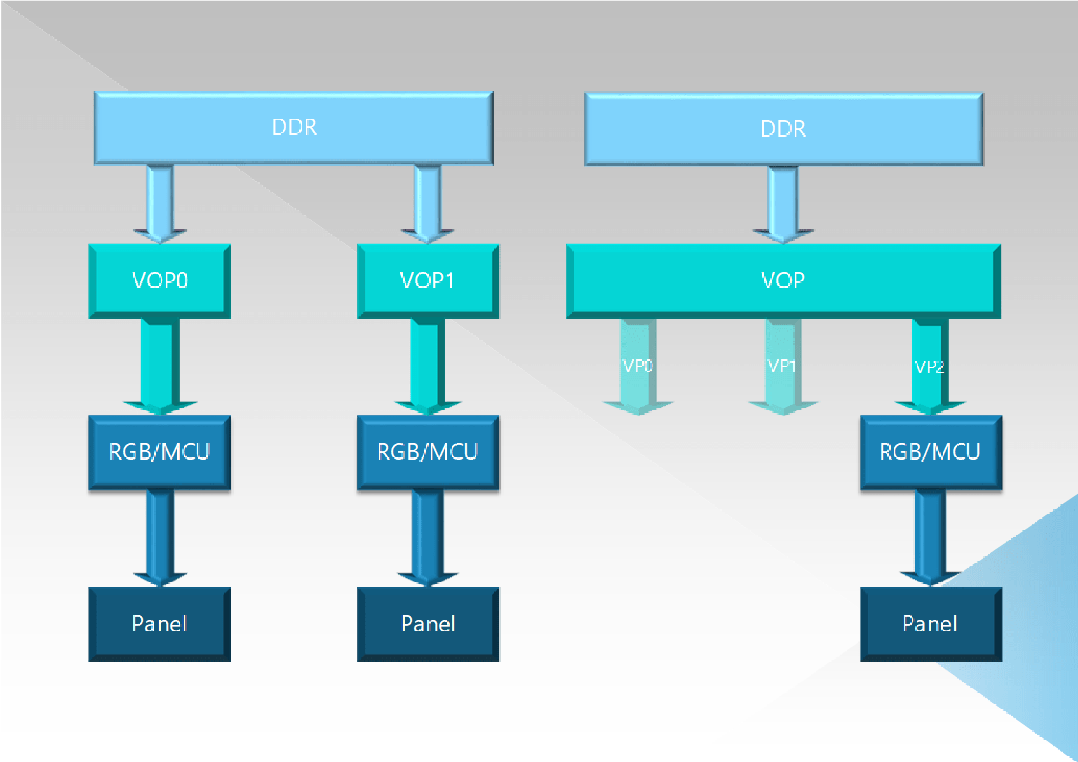
VOP 1.0/2.0 的 RGB/MCU 通路
VOP(Video Output Process)是 RK 平台的显示处理单元,存在 VOP 1.0 和 VOP 2.0 两种架构主要区别是对多显的支持方式不同,详细的介绍可以查阅文档《Rockchip_Developer_Guide_DRM_Display_Driver_CN》。左右框图分别对应 VOP 1.0 和 VOP 2.0 架构 RGB/MCU 接口的显示通路,VOP 会从 DDR 中读取图像数据并处理,再送到显示接口RGB/MCU 上,接口模块则会将图像数据转换为符合协议的数据流,最后传输到屏幕上显示。
4.2 Panel 配置
RGB panel 驱动可以参考 drivers/gpu/drm/panel/panel-simple.c 中的实现,下面为典型的 panel 节点配置:
/ {
   panel: panel {

      compatible = "simple-panel";
      bus-format = <MEDIA_BUS_FMT_RGB888_1X24>;
      backlight = <&backlight>;
      enable-gpios = <&gpio3 RK_PA6 GPIO_ACTIVE_LOW>;
      enable-delay-ms = <20>;
      reset-gpios = <&gpio3 RK_PB0 GPIO_ACTIVE_LOW>;
      reset-delay-ms = <10>;
      status = "okay";

      display-timings {

         native-mode = <&fx070_dhm11boe_timing>;

         fx070_dhm11boe_timing: timing0 {
           clock-frequency = <50000000>;
           hactive = <1024>;
           vactive = <600>;
           hback-porch = <140>;
           hfront-porch = <160>;
           vback-porch = <20>;
           vfront-porch = <20>;
           hsync-len = <20>;
           vsync-len = <2>;

           hsync-active = <0>;
           vsync-active = <0>;
           de-active = <0>;
           pixelclk-active = <0>;
         };
      };

      port {
         panel_in_rgb: endpoint {
           remote-endpoint = <&rgb_out_panel>;
         };
      };
   };

};

&backlight {
   pwms = <&pwm9 0 25000 0>;
   status = "okay";
};
bus-format 属性根据屏端支持的 display mode 配置,通常可以通过 panel datasheet 引脚定义说明及 panel驱动 IC 的显示模式支持等章节确定。DTS 中配置的宏定义详⻅ kernel 文件 include/uapi/linux/media-bus-format.h,与硬件连接的对应关系如下:
| Display Mode | Bus Format | Cycles Per Pixel |
|---|---|---|
| RGB888 (24bit) | MEDIA_BUS_FMT_RGB888_1X24 | 1 |
| RGB666 (18bit) | MEDIA_BUS_FMT_RGB666_1X18 | 1 |
| RGB666_CPADHI (18bit) | MEDIA_BUS_FMT_RGB666_1X24_CPADHI | 1 |
| RGB565 (16bit) | MEDIA_BUS_FMT_RGB565_1X16 | 1 |
| RGB565_CPADHI (16bit) | MEDIA_BUS_FMT_RGB565_1X24_CPADHI | 1 |
| RGB3x8 (8bit) | MEDIA_BUS_FMT_RGB888_3X8 MEDIA_BUS_FMT_RGB888_3X8 | 3 |
| RGB4x8(8bit) | MEDIA_BUS_FMT_RGB888_DUMMY_4X8 MEDIA_BUS_FMT_BGR888_DUMMY_4X8 | 4 |
backlight 节点的 pwms 配置需要根据硬件实际的连接情况修改,在显示图像前需要确保背光已经正常点亮。详⻅ pwm 模块参考文档《Rockchip_Developer_Guide_Linux_PWM_CN》。
enable-gpios/reset-gpios 和 enable-delay-ms/reset-delay-ms/prepare-delay-ms/unprepare-delay-ms/disable-delay-ms 配置需要根据 panel datasheet中上下电和复位的时序要求,以及实际硬件电路的设计来修改。
(可选)enable 引脚通常用于屏端供电的使能,gpio 配置取决于供电电路的具体设计。
(可选)reset 引脚通常屏端会直接引出,并在 datasheet 中说明触发复位功能的条件,gpio 配置取决于复位电路的具体设计。
(可选)enable-delay-ms/reset-delay-ms/prepare-delay-ms/unprepare-delay-ms/disable-delay-ms 根据 datasheet 的 power/reset/signal 时序要求配置。
display-timings 时序节点屏幕 datasheet 会提供推荐配置,用戶也可以根据具体的应用需求在指定的上下阈值区间内微调,下图为示例 panel 节点配置对应的 panel datasheet:
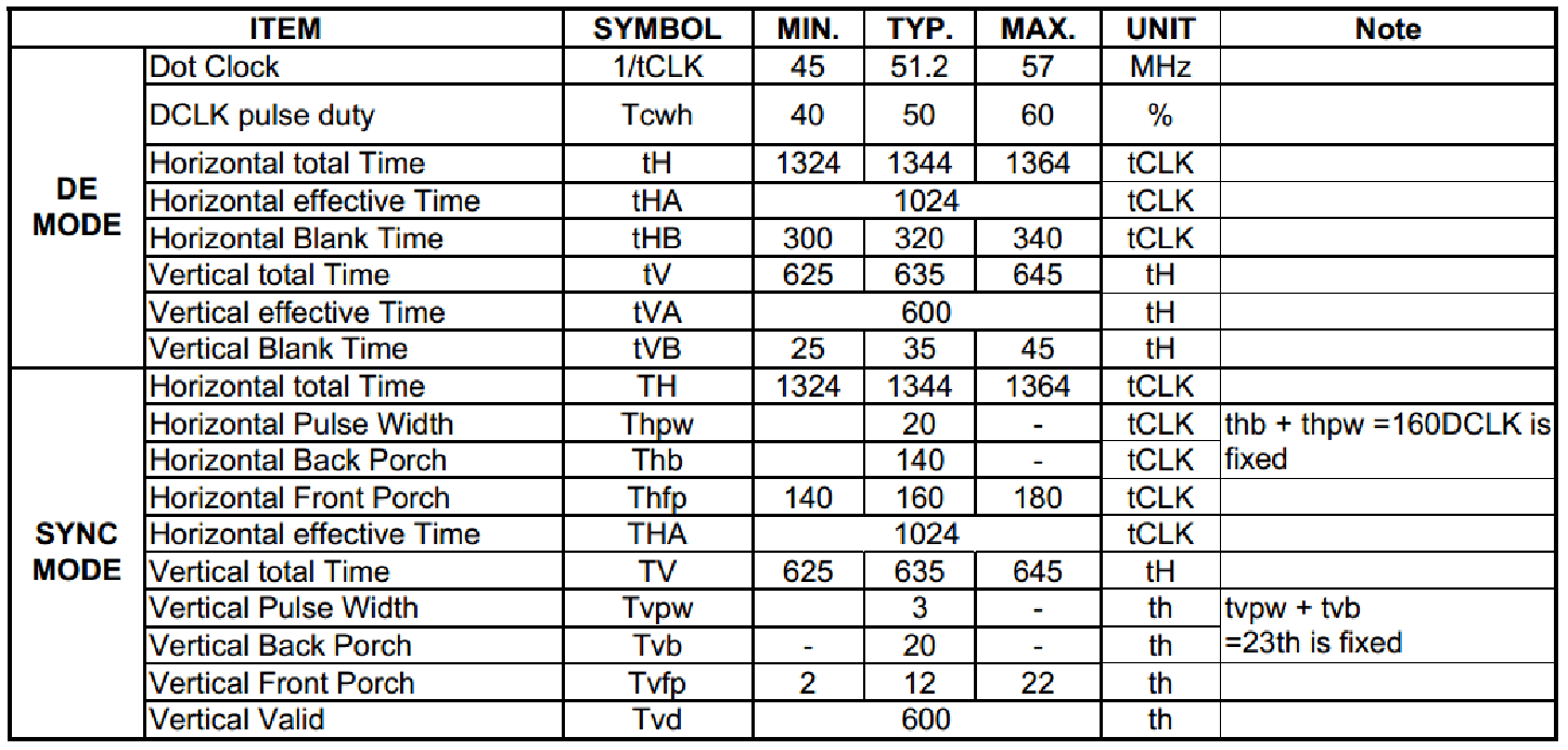
示例 Panel 时序参数原表
| 模式 | 参数 | 符号 | 最小 | 典型 | 最大 | 单位 | 注释 |
|---|---|---|---|---|---|---|---|
| DE | 像素时钟 | 1/tCLK | 45 | 51.2 | 57 | MHz | |
| DE | DCLK 占空比 | Tcwh | 40 | 50 | 60 | % | |
| DE | 水平总周期 | tH | 1324 | 1344 | 1364 | tCLK | |
| DE | 水平有效周期 | tHA | 1024 | tCLK | |||
| DE | 水平消隐 | tHB | 300 | 320 | 340 | tCLK | |
| DE | 垂直总周期 | tV | 625 | 635 | 645 | tH | |
| DE | 垂直有效周期 | tVA | 600 | tH | |||
| DE | 垂直消隐 | tVB | 25 | 35 | 45 | tH | |
| SYNC | 水平总周期 | TH | 1324 | 1344 | 1364 | tCLK | |
| SYNC | 水平脉宽 | Thpw | 20 | - | tCLK | thb + thpw = 160DCLK (固定) | |
| SYNC | 水平后肩 | Thb | 140 | - | tCLK | thb + thpw = 160DCLK (固定) | |
| SYNC | 水平前肩 | Thfp | 140 | 160 | 180 | tCLK | |
| SYNC | 水平有效周期 | THA | 1024 | tCLK | |||
| SYNC | 垂直总周期 | TV | 625 | 635 | 645 | th | |
| SYNC | 垂直脉宽 | Tvpw | 3 | - | th | tvpw + tvb = 23th (固定) | |
| SYNC | 垂直后肩 | Tvb | - | 20 | - | th | tvpw + tvb = 23th (固定) |
| SYNC | 垂直前肩 | Tvfp | 2 | 12 | 22 | th | |
| SYNC | 垂直有效 | Tvd | 600 | th |
同时 DRM 框架对于 display_timing 结构体及其变量的描述可以在文件 include/video/display_timing.h 中找到,如下所示:
/*
 * Single "mode" entry. This describes one set of signal timings a display can
 * have in one setting. This struct can later be converted to struct videomode

 * (see include/video/videomode.h). As each timing_entry can be defined as a
 * range, one struct display_timing may become multiple struct videomodes.
 *
 * Example: hsync active high, vsync active low
 *
 *            Active Video
 * Video ______________________XXXXXXXXXXXXXXXXXXXXXX_____________________
 *  |<- sync ->|<- back ->|<----- active ----->|<- front ->|<- sync..
 *  |    |  porch |        |  porch |
 *
 * HSync _|¯¯¯¯¯¯¯¯¯¯|___________________________________________|¯¯¯¯¯¯¯¯¯
 *

 * VSync ¯|__________|¯¯¯¯¯¯¯¯¯¯¯¯¯¯¯¯¯¯¯¯¯¯¯¯¯¯¯¯¯¯¯¯¯¯¯¯¯¯¯¯¯¯¯|_________
 */
struct display_timing {
   struct timing_entry pixelclock;

   struct timing_entry hactive; /* hor. active video */
   struct timing_entry hfront_porch; /* hor. front porch */
   struct timing_entry hback_porch; /* hor. back porch */
   struct timing_entry hsync_len; /* hor. sync len */

   struct timing_entry vactive; /* ver. active video */
   struct timing_entry vfront_porch; /* ver. front porch */
   struct timing_entry vback_porch; /* ver. back porch */

   struct timing_entry vsync_len; /* ver. sync len */

   enum display_flags flags; /* display flags */
};
对于 RGB/MCU 接口,display-timings 节点下 clock-frequency 属性值会决定 VOP 输出的帧率,计算中需要用到 drm 框架的时序属性 htotal 和 vtotal,此处截取部分说明,详⻅ include/drm/drm_modes.h。
帧率的计算则可以参考 drivers/gpu/drm/drm_modes.c 中 drm_mode_vrefresh() 函数的实现,设帧率为 fr则计算公式为:
fr = clock / (htotal * vtotal)
/**
 * struct drm_display_mode - DRM kernel-internal display mode structure

 * @hdisplay: horizontal display size
 * @hsync_start: horizontal sync start
 * @hsync_end: horizontal sync end
 * @htotal: horizontal total size
 * @hskew: horizontal skew?!
 * @vdisplay: vertical display size
 * @vsync_start: vertical sync start
 * @vsync_end: vertical sync end
 * @vtotal: vertical total size
 * @vscan: vertical scan?!
......
 *

 * The horizontal and vertical timings are defined per the following diagram.
 *
 * ::
 *
 *
 *          Active           Front      Sync       Back
 *         Region           Porch                  Porch
 *   <-----------------------><----------------><-------------><-------------->
 *    //////////////////////|
 *    ////////////////////// |
 *   ////////////////////// |.................. ................
 *                                  _______________

 *   <----- [hv]display ----->
 *   <------------- [hv]sync_start ------------>
 *   <--------------------- [hv]sync_end --------------------->
 *   <-------------------------------- [hv]total ----------------------------->*
 *
......
 */

/**
 * drm_mode_vrefresh - get the vrefresh of a mode
 * @mode: mode
 *
 * Returns:

 * @modes's vrefresh rate in Hz, rounded to the nearest integer. Calculates the
 * value first if it is not yet set.
 */
int drm_mode_vrefresh(const struct drm_display_mode *mode)
{
   unsigned int num, den;

   if (mode->htotal == 0 || mode->vtotal == 0)
      return 0;

   num = mode->clock;
   den = mode->htotal * mode->vtotal;


   if (mode->flags & DRM_MODE_FLAG_INTERLACE)
      num *= 2;
   if (mode->flags & DRM_MODE_FLAG_DBLSCAN)
      den *= 2;
   if (mode->vscan > 1)
      den *= mode->vscan;

   return DIV_ROUND_CLOSEST_ULL(mul_u32_u32(num, 1000), den);
}
EXPORT_SYMBOL(drm_mode_vrefresh);
4.2.1 SPI 初始化配置
有些 RGB 屏需要主控通过 SPI 接口发送指令以完成初始化流程,drivers/gpu/drm/panel/panel-simple.c 支持 3-wire 9-bit serial interface 协议:
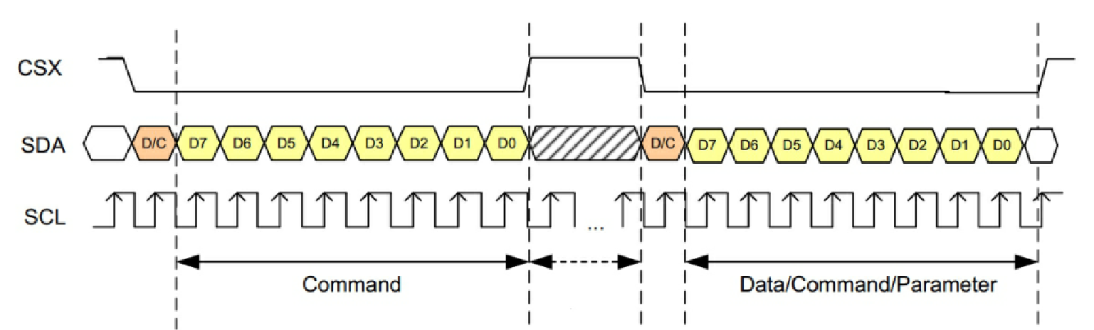
三线 9 位 SPI 初始化协议
由于 RK 平台 SPI 模块支持的数据传输粒度为 4/8/16 bit,上述协议为 9 bit 数据单元,因此在 panel-simple 驱动中是用 GPIO 模拟 SPI 来实现。
kernel-5.10 及以上内核版本的典型配置:
spi_gpio: spi-gpio {
   compatible = "spi-gpio";

   #address-cells = <0x1>;
   #size-cells = <0x0>;
   pinctrl-names = "default";
   pinctrl-0 = <&spi_gpio_pins>;
   spi-delay-us = <10>;
   status = "okay";

   sck-gpios = <&gpio4 RK_PA5 GPIO_ACTIVE_HIGH>;
   miso-gpios = <&gpio4 RK_PA7 GPIO_ACTIVE_HIGH>;
   mosi-gpios = <&gpio4 RK_PA6 GPIO_ACTIVE_HIGH>;
   cs-gpios = <&gpio4 RK_PA4 GPIO_ACTIVE_HIGH>;
   num-chipselects = <1>;


   /*
   * 320x480 RGB/MCU screen K350C4516T
   */
   panel: panel {
      compatible = "simple-panel-spi";
      reg = <0>;
      bus-format = <MEDIA_BUS_FMT_RGB666_1X18>;
      backlight = <&backlight>;
      enable-gpios = <&gpio3 RK_PA6 GPIO_ACTIVE_LOW>;
      enable-delay-ms = <20>;
      reset-gpios = <&gpio3 RK_PB0 GPIO_ACTIVE_LOW>;
      reset-delay-ms = <10>;

      prepare-delay-ms = <20>;
      unprepare-delay-ms = <20>;
      disable-delay-ms = <20>;
      init-delay-ms = <10>;
      width-mm = <217>;
      height-mm = <136>;
      rockchip,cmd-type = "spi";

      status = "okay";

      // type:0 is cmd, 1 is data
      panel-init-sequence = [
         /* type delay num val1 val2 val3 */
         00 00 01 e0
         01 00 01 00
         ......
         00 78 01 11
         00 00 01 29
      ];


      panel-exit-sequence = [
         //type delay num val1 val2 val3
         00 0a 01 28
         00 78 01 10
      ];

      display-timings {
         native-mode = <&kd050fwfba002_timing>;

         kd050fwfba002_timing: timing0 {
           /*
            * 10453500 for RGB666(18bit)
            */

           clock-frequency = <10453500>;
           hactive = <320>;
           vactive = <480>;
           hback-porch = <10>;
           hfront-porch = <5>;
           vback-porch = <10>;
           vfront-porch = <5>;
           hsync-len = <10>;
           vsync-len = <10>;
           hsync-active = <0>;
           vsync-active = <0>;
           de-active = <0>;

           pixelclk-active = <1>;
         };
      };

      port {
         panel_in_rgb: endpoint {
           remote-endpoint = <&rgb_out_panel>;
         };
      };
   };
};
需要打开配置项 CONFIG_SPI_GPIO,并根据硬件设计配置对应的 sck-gpios、miso-gpios、mosi-gpios 和
cs-gpios,详⻅驱动 drivers/spi/spi-gpio.c。panel 节点配置与上文基本相同,注意点如下:
compatible 修改为 ”simple-panel-spi“。
rockchip,cmd-type 需配置为 “spi”。
在 panel-init-sequence/panel-exit-sequence 填上相应的 init/deinit 序列。
kernel 4.19 及以下内核版本,SPI RGB 屏用到的 SDI/SCL/CS(注意实际上不支持 SDI,dts 中配置的 SDI 实为硬件上的 SDO,此为早期版本笔误)引脚直接在 simple-panel 驱动中用 gpio 模拟,不依赖第三方 SPI 驱动。示例如下:
panel: panel {
   compatible = "simple-panel";

   ......
   spi-sdi-gpios = <&gpio1 RK_PC7 GPIO_ACTIVE_HIGH>;
   spi-scl-gpios = <&gpio1 RK_PD0 GPIO_ACTIVE_HIGH>;
   spi-cs-gpios = <&gpio1 RK_PD1 GPIO_ACTIVE_HIGH>;
   ......
   rockchip,cmd-type = "spi";

   /* type:0 is cmd, 1 is data */
   panel-init-sequence = [
      /* type delay num val1 val2 val3 */
       00  00 01 e0
       ......
       00  78 01 11

       00  00 01 29
   ];

   panel-exit-sequence = [
      /* type delay num val1 val2 val3 */
      00 0a 01 28
      00 78 01 10
   ];
   ......
};
不同内核版本 SPI RGB 屏的参考配置如下:
kernel 4.19 及以下:arch/arm64/boot/dts/rockchip/rk3308-evb-ext-v10.dtsi
kernel 5.10 及以上:arch/arm64/boot/dts/rockchip/rk3562-evb1-lp4x-v10-rgb-k350c4516t.dts
4.3 RGB 接口
rgb 驱动对应文件 drivers/gpu/drm/rockchip/rockchip_rgb.c,参考 dts 配置如下:
&rgb {
   status = "okay";

   pinctrl-0 = <&rgb666_pins>;
   ports {
      port@1 {
         reg = <1>;


         rgb_out_panel: endpoint {
           remote-endpoint = <&panel_in_rgb>;
         };
      };
   };
};

//VOP 1.0
&rgb_in_vop {
   status = "okay";
};


//VOP 2.0
&rgb_in_vp0 {
   status = "okay";
};
对于 VOP 1.0 和 VOP 2.0 两种架构,RGB 接口相关节点的配置有所不同,参考配置:
VOP 1.0:arch/arm/boot/dts/rv1106-evb-ext-rgb-v10.dtsi。
VOP 2.0:可以参考 arch/arm64/boot/dts/rockchip/rk3562-evb1-lp4x-v10-rgb-FX070-DHM11BOE-A.dts。
pinctrl 配置需要根据实际的硬件连接确定,可以在 rkxxxx-pinctrl.dtsi/rvxxxx-pinctrl.dtsi 文件中找到各种线序对应的定义。
4.4 MCU 接口
mcu 接口及 mcu panel 驱动可以查看 drivers/gpu/drm/rockchip/rockchip_rgb.c,dts 配置与 rgb 接口基本相同,额外需要加上切换 mcu 模式的标志和 timing,参考配置如下:
&rgb {
   status = "okay";

   rockchip,data-sync-bypass;
   pinctrl-names = "default";
   /*
   * rgb3x8_pins_m0/rgb3x8_pins_m1 for RGB3x8(8bit)
   * rgb565_pins for RGB565(16bit)
   */
   pinctrl-0 = <&rgb565_pins>;

   /*
   * 320x480 RGB/MCU screen K350C4516T
   */
   mcu_panel: mcu-panel {
      /*

      * MEDIA_BUS_FMT_RGB888_3X8 for RGB3x8(8bit)
       * MEDIA_BUS_FMT_RGB565_1X16 for RGB565(16bit)
       */
      bus-format = <MEDIA_BUS_FMT_RGB565_1X16>;

      backlight = <&backlight>;
      enable-gpios = <&gpio1 RK_PA3 GPIO_ACTIVE_LOW>;
      enable-delay-ms = <20>;
      reset-gpios = <&gpio1 RK_PA4 GPIO_ACTIVE_LOW>;
      reset-value = <0>;
      reset-delay-ms = <10>;
      prepare-delay-ms = <20>;
      unprepare-delay-ms = <20>;
      disable-delay-ms = <20>;
      init-delay-ms = <10>;
      width-mm = <217>;
      height-mm = <136>;


      // type:0 is cmd, 1 is data
      panel-init-sequence = [
         //type delay num val1 val2 val3
          ......
          01  00 01 55 /*
                       * interface pixel format:
                       * 66 for RGB3x8(8bit)
                       * 55 for RGB565(16bit)
                       */
          ......
          01  00 01 a0 /*
                       * frame rate control:

                       * 70 (45hz) for RGB3x8(8bit)
                       * a0 (60hz) for RGB565(16bit)
                       */
          ......
          01  00 01 02 /*
                       * display function control:
                       * 32 for RGB
                       * 02 for MCU
                       */
          00  78 01 11
          00  32 01 29
          00  00 01 2c

      ];

      panel-exit-sequence = [
         //type delay num val1 val2 val3
          00  0a 01 28
          00  78 01 10
      ];

      display-timings {
         native-mode = <&kd050fwfba002_timing>;

         kd050fwfba002_timing: timing0 {
            /*
             * 7840125 for frame rate 45Hz
             * 10453500 for frame rate 60Hz
             */

            clock-frequency = <10453500>;
            hactive = <320>;
            vactive = <480>;
            hback-porch = <10>;
            hfront-porch = <5>;
            vback-porch = <10>;
            vfront-porch = <5>;
            hsync-len = <10>;
            vsync-len = <10>;
            hsync-active = <0>;
            vsync-active = <0>;
            de-active = <0>;

            pixelclk-active = <1>;
         };
      };

      port {
            panel_in_rgb: endpoint {
               remote-endpoint = <&rgb_out_panel>;
            };
         };
      };

      ports {
         rgb_out: port@1 {

            reg = <1>;
            #address-cells = <1>;
            #size-cells = <0>;

            rgb_out_panel: endpoint@0 {
               reg = <0>;
               remote-endpoint = <&panel_in_rgb>;
            };
         };
      };
   };
};


//VOP 1.0
&rgb_in_vop {
   status = "okay";
};

&vop {
   status = "okay";

   /*
    * Default config is as follows:
    *
    * mcu-pix-total = <9>;
   * mcu-cs-pst = <1>;
   * mcu-cs-pend = <8>;
   * mcu-rw-pst = <2>;

   * mcu-rw-pend = <5>;
   * mcu-hold-mode = <0>; // default set to 0
   *
   * To increase the frame rate, reduce all parameters because
   * the max dclk rate of mcu is 150M in rv1103/rv1106.
   */
   mcu-timing {
      mcu-pix-total = <5>;
      mcu-cs-pst = <1>;
      mcu-cs-pend = <4>;
      mcu-rw-pst = <2>;
      mcu-rw-pend = <3>;


      mcu-hold-mode = <0>; // default set to 0
   };
};

//VOP 2.0
&rgb_in_vp0 {
   status = "okay";
};

&vp0 {
   status = "okay";


   /*
   * Default config is as follows:
   *
   * mcu-pix-total = <9>;
   * mcu-cs-pst = <1>;
   * mcu-cs-pend = <8>;
   * mcu-rw-pst = <2>;
   * mcu-rw-pend = <5>;
   * mcu-hold-mode = <0>; // default set to 0
   *
   * To increase the frame rate, reduce all parameters because
   * the max dclk rate of mcu is 150M in rk3562.

   */
   mcu-timing {
      mcu-pix-total = <5>;
      mcu-cs-pst = <1>;
      mcu-cs-pend = <4>;
      mcu-rw-pst = <2>;
      mcu-rw-pend = <3>;

      mcu-hold-mode = <0>; // default set to 0
   };
};
对于 VOP 1.0 和 VOP 2.0 两种架构,MCU 接口相关节点的配置有所不同,参考配置:
VOP 1.0:arch/arm/boot/dts/rv1106-evb-ext-mcu-v10.dtsi。
VOP 2.0:可以参考 arch/arm64/boot/dts/rockchip/rk3562-evb1-lp4x-v10-mcu-k350c4516t.dts。驱动中会根据 rgb 节点下的 rockchip,data-sync-bypass 属性来切换 mcu 和 rgb 两种接口模式,不加该属性默认为 rgb 接口,使能后则切换到 mcu 接口。
在 kernel-5.10 及以上的版本,mcu 接口对应的 panel 配置推荐放在 rgb 节点下,kernel-4.19 及更早版本的内核,则作为独立的节点通过 simple-panel 驱动初始化。若将 simple-panel 驱动对应的 panel 节点移植到rgb 节点下需要注意:
确保 panel 节点命名为 mcu-panel,驱动中根据此去识别并解析 mcu panel 参数。
compatible 属性可以删除,无需配置。
mcu panel 通常需要通过初始化序列来初始化 display mode/pixel format/frame rate 等配置(具体由 panel的驱动 IC 确定),以及通过去初始化序列来确保 panel 关闭或进入 low-power 模式等。相关 panel-init-sequence 和 panel-exit-sequence 属性的注意点如下:
序列由屏厂提供,通常需要从 c 文件转换为 DTS 配置。
序列每行从左往右依次为:指令类型cmd/data、延迟时间(ms)、数据⻓度(byte)、数据。
帧率的配置通常也在序列初始化阶段进行,需要跟《Panel 配置》中计算出的帧率相对应。下面是示例驱动 IC 手册中的说明:
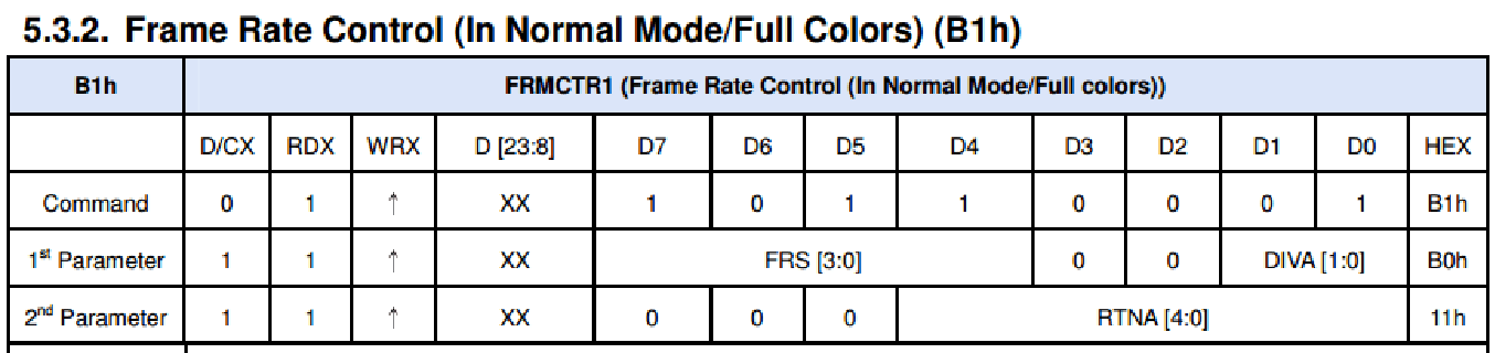
FRMCTR1 帧率控制寄存器原表
| FRMCTR1 (B1h) | D/CX | RDX | WRX | D[23:8] | D7..D0 | HEX |
|---|---|---|---|---|---|---|
| 指令 | 0 | 1 | ↑ | XX | 1 0 1 1 0 0 0 1 | B1h |
| 第 1 参数 | 1 | 1 | ↑ | XX | FRS[3:0] / 0 / 0 / DIVA[1:0] | B0h |
| 第 2 参数 | 1 | 1 | ↑ | XX | 0 / 0 / 0 / RTNA[4:0] | 11h |
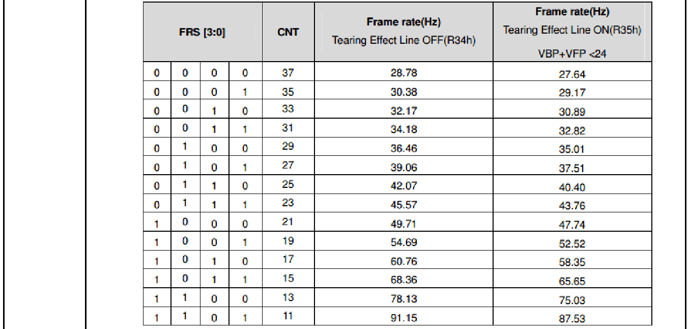
FRS 与帧率对应原表摘图
| FRS[3:0] | CNT | Hz / TE OFF (R34h) | Hz / TE ON (R35h), VBP+VFP <24 |
|---|---|---|---|
| 0000 | 37 | 28.78 | 27.64 |
| 0001 | 35 | 30.38 | 29.17 |
| 0010 | 33 | 32.17 | 30.89 |
| 0011 | 31 | 34.18 | 32.82 |
| 0100 | 29 | 36.46 | 35.01 |
| 0101 | 27 | 39.06 | 37.51 |
| 0110 | 25 | 42.07 | 40.40 |
| 0111 | 23 | 45.57 | 43.76 |
| 1000 | 21 | 49.71 | 47.74 |
| 1001 | 19 | 54.69 | 52.52 |
| 1010 | 17 | 60.76 | 58.35 |
| 1011 | 15 | 68.36 | 65.65 |
| 1100 | 13 | 78.13 | 75.03 |
| 1101 | 11 | 91.15 | 87.53 |
mcu-timing 用于配置 MCU 接口 normal mode 控制信号 CSN/WEN/REN 的时序,各属性分别对应下图中各区间的时间。详细时序图及各区间的具体要求摘自示例 dts 配置对应 panel 模组的 datasheet。下面将介绍mcu-timing 中各属性及 display-timings 中 clock-frequency 属性的配置方法。
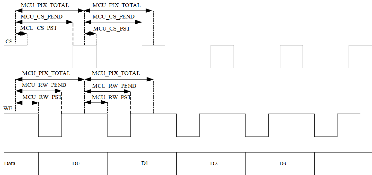
MCU normal mode 控制信号时序
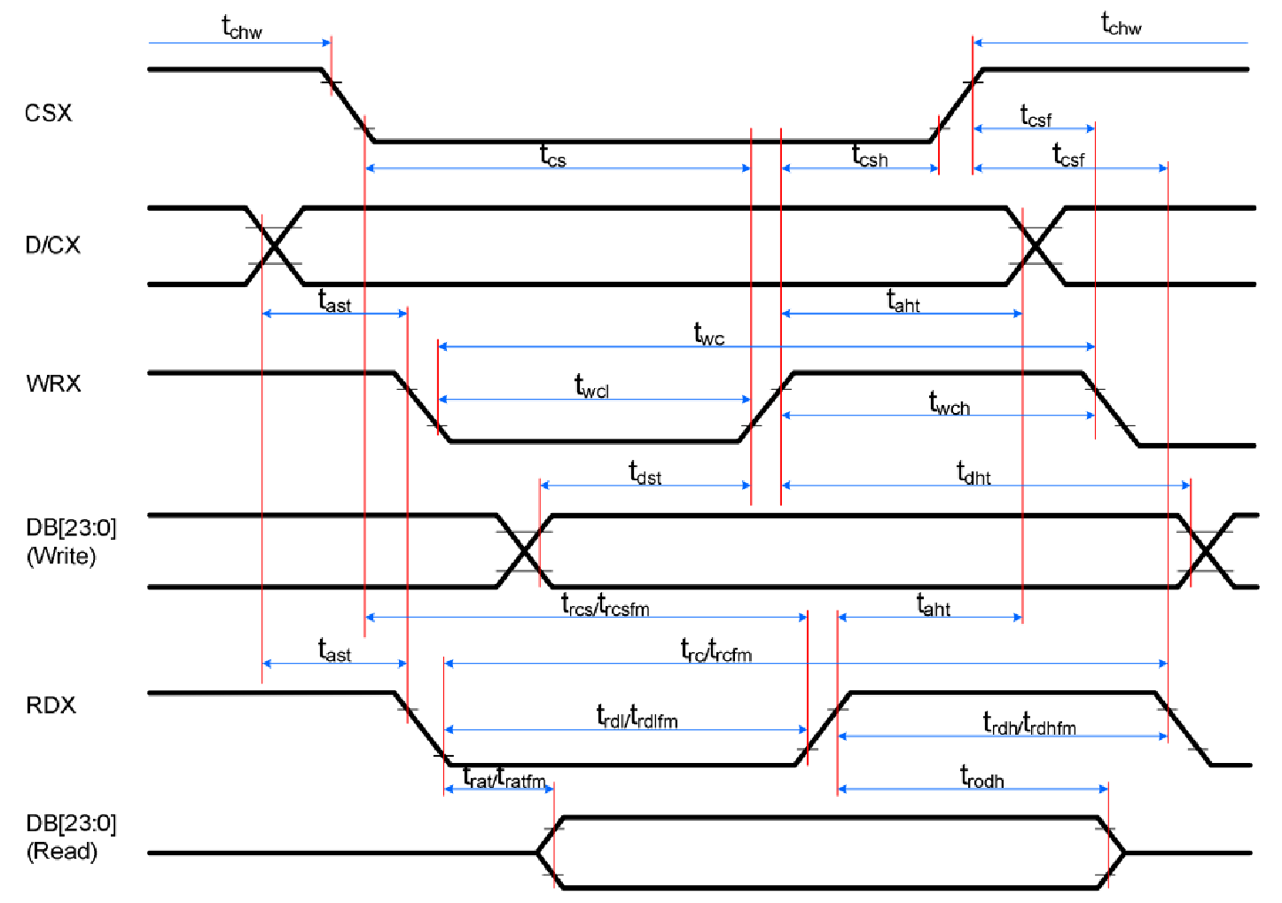
Panel 写入/读取时序
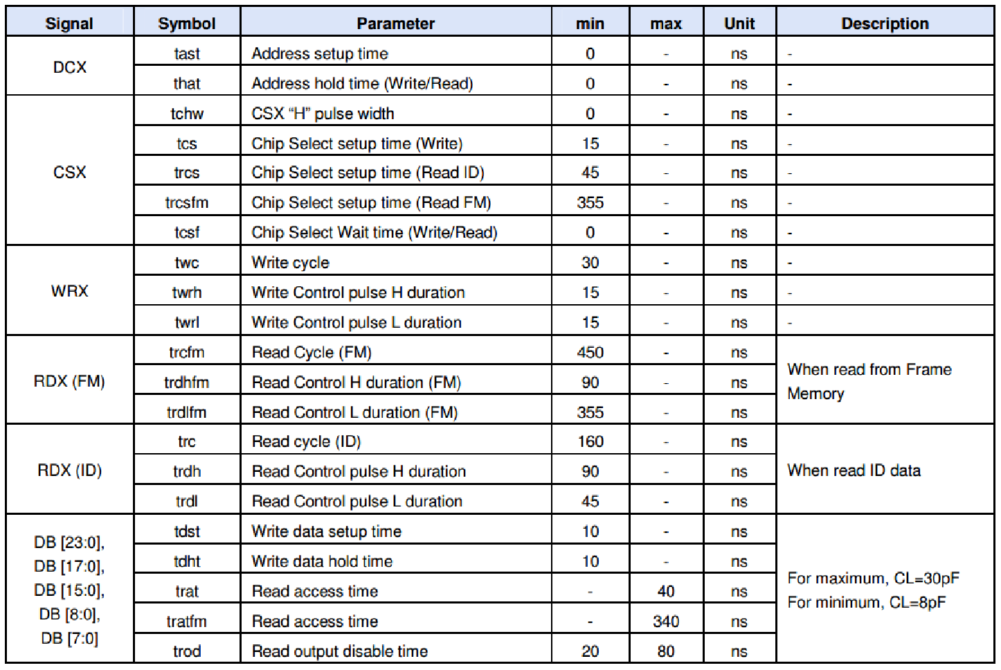
Panel 驱动 IC 时序要求原表
| 信号 | 符号 | 参数 | 最小 | 最大 | 单位 | 说明 |
|---|---|---|---|---|---|---|
| DCX | tast | 地址建立时间 | 0 | - | ns | - |
| DCX | that | 地址保持时间(写/读) | 0 | - | ns | - |
| CSX | tchw | CSX 高脉宽 | 0 | - | ns | - |
| CSX | tcs | 片选建立(写) | 15 | - | ns | - |
| CSX | trcs | 片选建立(读 ID) | 45 | - | ns | - |
| CSX | trcsfm | 片选建立(读 FM) | 355 | - | ns | - |
| CSX | tcsf | 片选等待(写/读) | 0 | - | ns | - |
| WRX | twc | 写周期 | 30 | - | ns | - |
| WRX | twrh | 写控制高电平时间 | 15 | - | ns | - |
| WRX | twrl | 写控制低电平时间 | 15 | - | ns | - |
| RDX (FM) | trcfm | 读周期(FM) | 450 | - | ns | 读取帧存储器 |
| RDX (FM) | trdhfm | 读控制高电平时间(FM) | 90 | - | ns | 读取帧存储器 |
| RDX (FM) | trdlfm | 读控制低电平时间(FM) | 355 | - | ns | 读取帧存储器 |
| RDX (ID) | trc | 读周期(ID) | 160 | - | ns | 读取 ID 数据 |
| RDX (ID) | trdh | 读控制高电平时间 | 90 | - | ns | 读取 ID 数据 |
| RDX (ID) | trdl | 读控制低电平时间 | 45 | - | ns | 读取 ID 数据 |
| DB[23:0], DB[17:0], DB[15:0], DB[8:0], DB[7:0] | tdst | 写数据建立 | 10 | - | ns | 最大值:CL=30pF;最小值:CL=8pF |
| DB[23:0], DB[17:0], DB[15:0], DB[8:0], DB[7:0] | tdht | 写数据保持 | 10 | - | ns | 最大值:CL=30pF;最小值:CL=8pF |
| DB[23:0], DB[17:0], DB[15:0], DB[8:0], DB[7:0] | trat | 读访问时间 | - | 40 | ns | 最大值:CL=30pF;最小值:CL=8pF |
| DB[23:0], DB[17:0], DB[15:0], DB[8:0], DB[7:0] | tratfm | 读访问时间 | - | 340 | ns | 最大值:CL=30pF;最小值:CL=8pF |
| DB[23:0], DB[17:0], DB[15:0], DB[8:0], DB[7:0] | trod | 读输出禁用时间 | 20 | 80 | ns | 最大值:CL=30pF;最小值:CL=8pF |
设变量 ptotal 为 mcu-timing 中 mcu-pix-total 的值,查表可知 panel datasheet 中要求MCU_PIX_TOTAL 区间时间不小于 tmin:
(panel datasheet 中 twc = 40 而驱动 ic datasheet twc = 30,取两者中的较大值)
tmin = T_CHW + T_AST + T_WC + T_CHW = 40 ns
对于示例 panel,同时支持 MEDIA_BUS_FMT_RGB888_3X8 和 MEDIA_BUS_FMT_RGB565_1X16 两种mode,Cycles Per Pixel 值(指将一个 pixel 的数据分成 n 个 cycle 去发送,详⻅《Panel 配置》章节)设为 cpp,则可以计算出两者对应的理论帧率上限(分别设为 frs-max 和 frp-max):
fr < 1000000000 / (htotal * ptotal * cpp * tmin)
htotal = hactive + hback-porch + hfront-porch + hsync-len = 345
vtotal = vactive + vback-porch + vfront-porch + vsync-len = 505
fr_s-max < 1000000000 / (345 * 505 * 3 * 40) ≈ 47.83 Hz
fr_p-max < 1000000000 / (345 * 505 * 1 * 40) ≈ 143.49 Hz
校对提示:原文通式分母写 ptotal,而随后的数值代入使用 505(上文 vtotal)。这里保留原式与原计算,未擅改,请核对。
因此,串行 rgb3x8 模式的帧率 frs = 45(Hz),并行 rgb1x16 模式的帧率 frp = 60(Hz)。
(下文变量的下缀 s 表示 serial 串行,p 表示 parallel 并行,不再赘述)
同时也可算出两者 display-timings 配置中 clock-frequency 属性的值:
clock_s = fr_s * htotal * vtotal = 45 * 345 * 505 = 7840125
clock_p = fr_p * htotal * vtotal = 60 * 345 * 505 = 10453500
每个平台 mcu 接口的 dclk 都会有最大值限制,详⻅ drivers/gpu/drm/rockchip/rockchip_rgb.c 驱动中的 mcu_max_dclk_rate 属性,通常为 150000000 Hz,驱动中相应的检查逻辑详⻅rockchip_rgb_encoder_mode_valid() 函数。
根据 dclkmax 和初始化序列中配置的帧率(设为变量 fr,值通常为 60Hz),可以算出 ptotal 的最大值:
ptotal_max < dclk_max / (cpp * clock) - 1
ptotal_s-max < 150000000 / (3 * 7840125) - 1 ≈ 5.38
ptotal_p-max < 150000000 / (1 * 10453500) - 1 ≈ 13.35
实际的 ptotal 取两者较小值 ptotal = 5,同时由时序图可确定 mcu-timing 的其他属性值。
最后,还需要根据 datasheet 时序要求对计算出的实际值作校验。
MCU 接口的实际 dclk 并不是 display-timings 配置中 clock-frequency 属性的值,还和 mcu-timing 中mcu-pix-total 配置和 Cycles Per Pixel 值有关:
dclk = clock * cpp * (ptotal + 1)
dclk_s = 7840125 * 3 * 6 = 141122250
dclk_p = 10453500 * 1 * 6 = 62721000
上述 dclk 值均未超过 dclkmax,同时可以计算出 MCU_PIX_TOTAL 区间实际时间:
t_s = (ptotal + 1) * 1000000000 / dclk_s ≈ 42.52 ns
t_p = (ptotal + 1) * 1000000000 / dclk_p ≈ 95.66 ns
上述 MCU_PIX_TOTAL 区间时间 t 均满足大于 40 ns 的要求。
4.4.1 MCU Bypass Timing 配置
早期支持 MCU 接口的平台,如 RK3308 和 PX30 等,bypass mode 的 timing 配置跟 normal mode 是一致的。在RK3562 及之后的平台,IC 在设计上进行了优化,驱动中会有一组默认的 bypass mode timing 用于满足大多数情况下 bypass mode 中 write/read 操作的需要,详⻅ drivers/gpu/drm/rockchip/rockchip_vop_reg.c 和drivers/gpu/drm/rockchip/rockchip_vop2_reg.c 中结构体 vop_mcu_bypass_cfg 的相关定义,如:
static struct rockchip_mcu_timing rk3506_mcu_bypass_timing = {
   .mcu_pix_total = 26,
   .mcu_cs_pst = 3,

   .mcu_cs_pend = 24,
   .mcu_rw_pst = 6,
   .mcu_rw_pend = 15,
};

static const struct vop_mcu_bypass_cfg rk3506_mcu_bypass_cfg = {
   .timing = &rk3506_mcu_bypass_timing,
   .dclk_rate = 120000000,
};
如果默认的 bypass mode timing 无法满足应用场景的需要,支持在 dts 中指定(参考 arch/arm/boot/dts/rk3506g-evb1-v10-mcu-k350c4516t.dts):
&vop {
   mcu-timing {

      mcu-pix-total = <5>;
      mcu-cs-pst = <1>;
      mcu-cs-pend = <4>;
      mcu-rw-pst = <2>;
      mcu-rw-pend = <3>;

      mcu-hold-mode = <0>;
   };

   mcu-bypass-timing {
      mcu-pix-total = <9>;
      mcu-cs-pst = <1>;
      mcu-cs-pend = <8>;

      mcu-rw-pst = <2>;
      mcu-rw-pend = <7>;

      mcu-hold-mode = <0>;
   };
};
需要注意的是,bypass mode 中可能会涉及 MCU read 操作,而通常情况下,MCU read timing 的 min 限制会大于 MCU write timing(可以参考前一章节的示例 datasheet),所以 mcu-bypass-timing 通常会以datasheet 中 read timing 的限制去计算和配置,以同时兼容 write/read 操作的时序要求。
4.4.2 MCU Frame Write/Read
在 MCU normal mode 下,可以通过 frame write/read 功能在帧间去进行主控和 panel 间的指令交互行为,用于读取 panel 的状态寄存器、修改显示的起始位置等,通常用于静电压测或满足一些特定 panel 逐帧更新显示起始位置的需要等场景。
使能该功能需要在 dts 中配置 panel-frame-sequence 序列,可以参考 arch/arm/boot/dts/rk3506g-evb1-v10-mcu-k350c4516t.dts,示例如下:
&rgb {
   ......
   mcu_panel: mcu-panel {

      ......
      panel-frame-sequence = [
         //type delay num val1 val2 val3
          00  00 01 0a
          02  00 01 0a
          02  00 01 0a
          00  00 01 2c
      ];
      ......
   };
   ......
};
帧间的 write/read 操作是在 drivers/gpu/drm/rockchip/rockchip_rgb.c 中实现的:
static void mcu_interframe_work_func(struct work_struct *work)
{
   struct rockchip_mcu_panel *mcu_panel =

      container_of(work, struct rockchip_mcu_panel, interframe_work);
   struct drm_panel *panel = &mcu_panel->base;
   struct drm_display_mode *mode = mcu_panel->desc->mode;
   struct drm_crtc *crtc = mcu_panel->encoder->crtc;
   u32 timeout = DIV_ROUND_CLOSEST_ULL(1000, drm_mode_vrefresh(mode));
   int ret;

   ret = rockchip_drm_wait_vact_end(crtc, timeout);
   if (ret) {
      DRM_DEV_ERROR(panel->dev, "wairt vact end timed out\n");
      return;
   }


   ret = rockchip_mcu_panel_xfer_mcu_cmd_seq(mcu_panel, mcu_panel->desc->frame_seq);
   if (ret) {
      DRM_DEV_ERROR(panel->dev, "failed to send frame cmds seq\n");
      return;
   }

   schedule_work(&mcu_panel->interframe_work);
};
如果有特定的应用需求,可以自行修改上述 work 的实现。
5. 调试流程
1. 确认 rgb/mcu 接口各 pin 脚的硬件连接,需要注意每个平台 pin 脚的映射方式可能会有所不同,具体看上文
《硬件连接》章节。
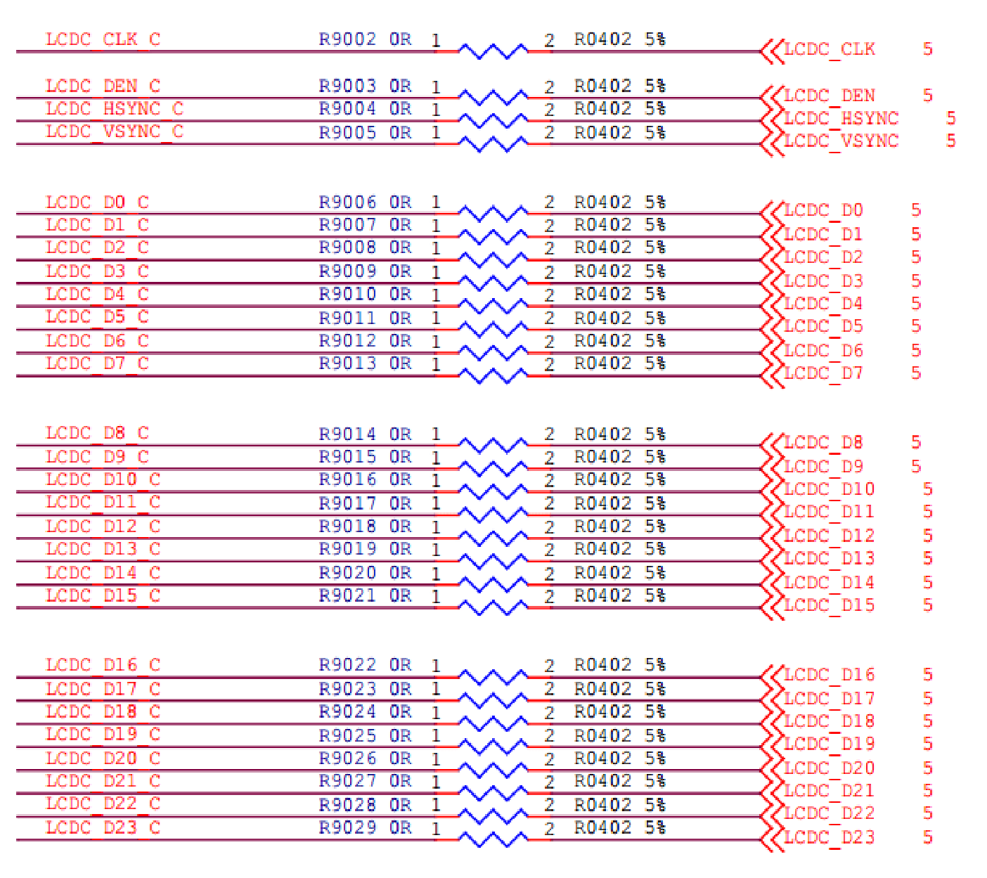
RGB/MCU 引脚连接示例
2. 根据 panel datasheet 正确配置 enable/reset 控制引脚极性和上电时序,以及背光所用到的 pwm 通道。若为mcu 屏,还需要配置正确的初始化序列。

复位、使能及背光 PWM 连接示例
3. 确保背光已点亮的情况下,需再确认下 enable/reset 控制引脚是否为正确的电平,若实际测量仍非预期值,则确认下 iomux 是否正确配置为 GPIO。
6. 常⻅问题
6.1 RGB/MCU 屏可以显示图像但屏幕上有噪点或者存在显示错位现象
答:可以尝试翻转下 dclk 时钟极性,对应 display-timings 下的 pixelclk-active 属性,可以改变 dclk 与 data 信号的相对相位。
display-timings {
   native-mode = <&fx070_dhm11boe_timing>;


   fx070_dhm11boe_timing: timing0 {
      clock-frequency = <50000000>;
      hactive = <1024>;
      vactive = <600>;
      hback-porch = <140>;
      hfront-porch = <160>;
      vback-porch = <20>;
      vfront-porch = <20>;
      hsync-len = <20>;
      vsync-len = <2>;
      hsync-active = <0>;
      vsync-active = <0>;

      de-active = <0>;
      pixelclk-active = <0>; // 1 翻转,0 不翻转
   };
};