
ArmSoM applicability
This is a Rockchip platform reference, not an ArmSoM hardware test report. The source product table covers RK3126, RK3128 and RK3288 (Linux 4.4), plus RK3326/PX30, RK3368 and RK356X (Linux 4.19 and later); the support table also lists RK3562. Adaptation requires checking exposed LVDS signals, PHY/VP routing, the target SDK driver, panel timing, supplies and backlight. This is not a claim that every ArmSoM board supports LVDS. No hardware validation was performed.
The Chinese and English PDFs are both V1.2.0, with 22 and 24 pages respectively. Chinese follows the Chinese source; English follows the English source; Russian translates the full English body. Corresponding technical sections and source differences are preserved. Chinese uses Chinese original figures, while English and Russian use English original figures.
Source discrepancies: scenario-table row 4 names LVDS0 twice, while the later diagram and configuration use LVDS0/LVDS1. The original table values are retained for verification. The RK3288 vopl example lacks a final semicolon; it has not been silently repaired.
Source product versions
| SoC | Linux |
|---|---|
| RK3126 | 4.4 |
| RK3128 | 4.4 |
| RK3288 | 4.4 |
| RK3326/PX30 | 4.19 and later |
| RK3368 | 4.19 and later |
| RK356X | 4.19 and later |
1. Basic Concepts
LVDS (Low Voltage Differential Signaling) is a low-voltage differential signal transmission technology used to transmit signals in high-speed serial data communication. It is widely applied in fields such as display, image transmission, and data communication.
LVDS is a physical layer signal transmission technology that defines electrical characteristics and interface standards. The VESA and JEIDA organizations stipulate the transmission methods of LVDS on the data link. According to the amount of transmitted data and the transmission sequence, it can be divided into JEIDA-18 , JEIDA-24 , VESA-24 , etc.
For LVDS, 7 bits of data can be transmitted in one clock cycle. The following briefly introduces the timings of various common LVDS formats.
1. JEIDA-18
Slot     0    1     2     3     4     5    6
       __________                _________________
Clock         \_______________________/

       ______ ______ ______ ______ ______ ______ ______
DATA0 ><__G0__><__R5__><__R4__><__R3__><__R2__><__R1__><__R0__><
DATA1 ><__B1__><__B0__><__G5__><__G4__><__G3__><__G2__><__G1__><
DATA2 ><_CTL2_><_CTL1_><_CTL0_><__B5__><__B4__><__B3__><__B2__><
2. JEIDA-24
Slot     0    1     2     3     4     5    6
      ___________                _________________
Clock         \_______________________/

      ______ ______ ______ ______ ______ ______ ______
DATA0 ><__G2__><__R7__><__R6__><__R5__><__R4__><__R3__><__R2__><
DATA1 ><__B3__><__B2__><__G7__><__G6__><__G5__><__G4__><__G3__><
DATA2 ><_CTL2_><_CTL1_><_CTL0_><__B7__><__B6__><__B5__><__B4__><
DATA3 ><_CTL3_><__B1__><__B0__><__G1__><__G0__><__R1__><__R0__><
3. VESA-24
Slot     0    1     2     3     4     5    6
      ___________                _________________

Clock         \_______________________/
       ______ ______ ______ ______ ______ ______ ______
DATA0 ><__G0__><__R5__><__R4__><__R3__><__R2__><__R1__><__R0__><
DATA1 ><__B1__><__B0__><__G5__><__G4__><__G3__><__G2__><__G1__><
DATA2 ><_CTL2_><_CTL1_><_CTL0_><__B5__><__B4__><__B3__><__B2__><
DATA3 ><_CTL3_><__B7__><__B6__><__G7__><__G6__><__R7__><__R6__><
Among them, CTL2 is the DE enable signal, CTL1 is the VSYNC field sync signal, and CTL0 is the HSYNC line sync signal. CTL3 is a reserved signal for additional purposes and can generally be ignored.
In the panel node of DTS, the LVDS format to be adopted can be specified through the bus-format attribute, and the corresponding relationships are as follows:
MEDIA_BUS_FMT_RGB666_1X7X3_SPWG : jeida-18
MEDIA_BUS_FMT_RGB888_1X7X4_JEIDA : jeida -24
MEDIA_BUS_FMT_RGB888_1X7X4_SPWG : vesa-24
2. Electrical Characteristics
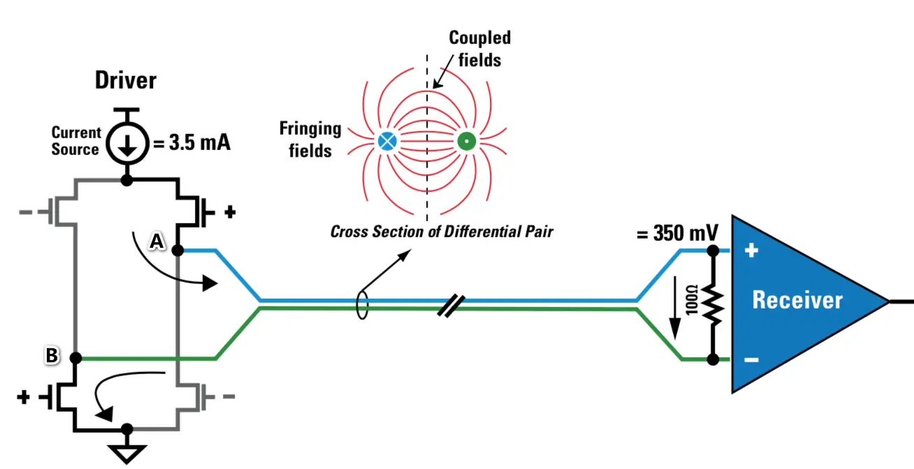
The typical implementation circuit of the LVDS driver is shown in the figure above. Essentially, it is a differential amplifier circuit driven by a constant current source.
First, consider the DC output characteristics. For an ideal differential amplifier circuit, the common-mode voltage Vcm can be expressed in the following form:
V_cm = (U_a + U_b) / 2
where U_a is the DC voltage of A to ground in the figure, and U_b is the DC voltage of B to ground in the figure.
For an ideal differential amplifier circuit, it is considered that U_a = U_b, that is, there is no voltage difference across the 100 Ω resistor at the receiving end, showing the characteristic of DC isolation.
Then consider the AC output characteristics. The small AC signal u_ab generated at both ends of AB produces a voltage drop on both sides of the 100 Ω resistor at the receiving end, showing the characteristic of AC passing.
A common requirement is to adjust the driving strength of LVDS. Taking enhancing the driving strength as an example, there are various implementation methods, such as increasing the current of the constant current source and increasing the load resistance.
The above analysis is from the perspective of circuit analysis. In practical applications, some LVDS PHYs provide additional configurations to complete these operations. For example, the driving strength of LVDS can be increased by increasing the differential voltage u_ab (the higher the voltage difference, the greater the current).
In practical applications, the impact of the transmission line also needs to be considered. Optimizing the capacitance and resistance on the differential line (making them smaller) can also enhance the driving strength of LVDS to a certain extent.
3. Platform Support
| Platform | Support LVDS0 | Support LVDS1 |
|---|---|---|
| RK3568 | Y | Y |
| RK3567 | Y | Y |
| RK3566 | Y | N |
| RK3562 | Y | N |
| RK3368 | Y | N |
| RK3326 / PX30 | Y | N |
| RK3288 | Y | Y |
| RK3128 | Y | N |
| RK3126 | Y | N |
4. Application Scenario Overview
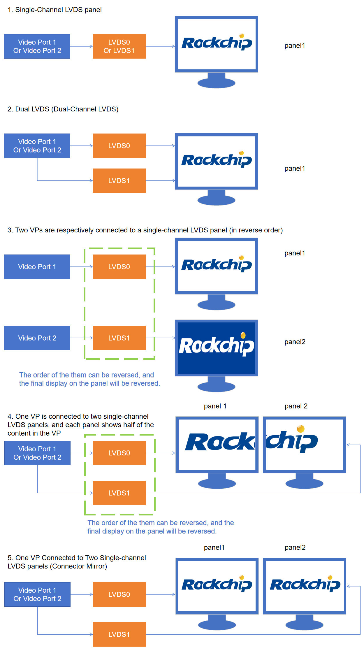
According to different usage scenarios, the usage of LVDS can be summarized in the following table:
| No. | Panels | LVDS interfaces | Video Port allocation | Maximum resolution | Description | Reference configuration |
|---|---|---|---|---|---|---|
| 1 | 1 | LVDS0 / LVDS1 | VP1 → LVDS0/1; VP2 → LVDS0/1 | 1280x800 | Single-channel LVDS panel | rk3567-evb2-lp4x-v10-single-channel-lvds.dts rk3568-evb1-ddr4-v10-single-channel-lvds.dts |
| 2 | 1 | LVDS0 + LVDS1 | VP1 → LVDS0 + LVDS1; VP2 → LVDS0 + LVDS1 | 1920x1080 | Dual LVDS, dual-channel LVDS | rk3567-evb2-lp4x-v10-dual-channel-lvds.dts |
| 3 | 2 | LVDS0 + LVDS1 | VP1 → LVDS0, VP2 → LVDS1; VP2 → LVDS0, VP1 → LVDS1 | 1280x800 per panel | Two VPs, each connected to one single-channel LVDS panel | rk3567-evb2-lp4x-v10-two-vp-two-separate-single-channel-lvds.dts rk3568-evb1-ddr4-v10-two-vp-two-separate-single-channel-lvds.dts |
| 4 | 2 | LVDS0 + LVDS1 | VP1 → LVDS0, VP1 → LVDS0; VP2 → LVDS0, VP2 → LVDS0 | 1280x800 per panel | One VP, two single-channel LVDS panels, each displaying half the VP content | rk3567-evb2-lp4x-v10-one-vp-two-single-channel-lvds.dts rk3568-evb1-ddr4-v10-one-vp-two-single-channel-lvds.dts |
| 5 | 2 | LVDS0 + LVDS1 | VP1 → LVDS0 + LVDS1; VP2 → LVDS0 + LVDS1 | 1280x800 per panel | One VP, two single-channel LVDS panels, both showing identical content (connector mirror) | See the relevant section in this article |
The actual effects of these 5 scenarios are shown in the following figure:
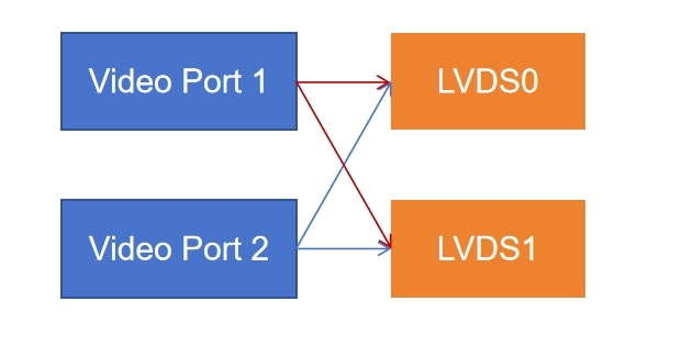
For RK356X, the allocation relationship between the Video Port and LVDS is shown in the following figure:
5. LVDS Configuration Examples for Different Scenarios
In this section, configuration examples of different LVDS will be introduced. Although there are various combinations of LVDS outputs, in fact, only the following two points need to be considered:
Whether it is dual-channel LVDS, that is, Dual LVDS.
Which VP the actual LVDS corresponds to.
For Dual LVDS, two LVDS nodes need to be enabled, and the dual-channel attribute needs to be added to the LVDS0 node to indicate that Dual LVDS is used.
&lvds0 {
   status = "okay";

   dual-channel;
};
In addition, it is necessary to confirm which VP the LVDS corresponds to. For Dual LVDS, both LVDS0 and LVDS1 use VP1 or both use VP2 as the output. For the remaining cases, the configuration is carried out according to the specific scenario:
/*
 * Example 1: Two VPs are respectively connected to a single-channel LVDS panel

 * VP1 -> LVDS0, VP2 -> LVDS1
 */
&lvds0_in_vp1 {
   status = "okay";
};

&lvds1_in_vp2 {
   status = "okay";
};

/*
 * Example 2: Two VPs are respectively connected to a single-channel LVDS panel (in reverse
order)

 * VP2 -> LVDS0, VP1 -> LVDS1
 */
&lvds0_in_vp2 {
   status = "okay";
};

&lvds1_in_vp1 {
   status = "okay";
};
5.1 Single-channel LVDS Configuration
When configuring single-channel LVDS, the following parameters need to be confirmed:
The panel timing, output format, corresponding Enable pin, and PWM backlight pin
Whether to output from LVDS0 or LVDS1
Whether to output from VP1 or VP2 to LVDS
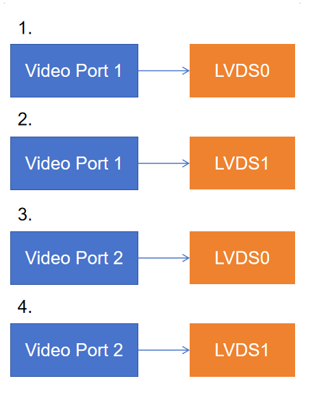
For single-channel LVDS on RK356X, there are 4 allocation relationships between LVDS and VP, as shown in the following figure:
Taking VP1 outputting LVDS0 as an example, the following briefly introduces the DTS configuration process:
1. Set the panel node, configure the panel timing, output format, Enable, and backlight pins, and associate the panel with the LVDS node:
panel {
   compatible = "simple-panel";

   backlight = <&backlight>;
   power-supply = <&vcc3v3_lcd0_n>;
   enable-delay-ms = <20>;
   prepare-delay-ms = <20>;
   unprepare-delay-ms = <20>;
   disable-delay-ms = <20>;
   bus-format = <MEDIA_BUS_FMT_RGB666_1X7X3_SPWG>;
   width-mm = <217>;
   height-mm = <136>;

   display-timings {
      native-mode = <&timing0>;
      timing0: timing0 {

         clock-frequency = <67000000>;
         hactive = <800>;
         vactive = <1280>;
         hback-porch = <60>;
         hfront-porch = <60>;

         vback-porch = <4>;
         vfront-porch = <2>;
         hsync-len = <8>;
         vsync-len = <8>;
         hsync-active = <0>;
         vsync-active = <0>;
         de-active = <0>;
         pixelclk-active = <0>;
      };
   };

   ports {

      #address-cells = <1>;
      #size-cells = <0>;
      port@0 {
         reg = <0>;
         panel_in_lvds0: endpoint {
           remote-endpoint = <&lvds0_out_panel>;
         };
      };
   };
};
2. Enable the corresponding LVDS node and associate it with the panel node:
&lvds0 {
   status = "okay";
   ports {

      port@1 {
         reg = <1>;
         lvds0_out_panel: endpoint {
           remote-endpoint = <&panel_in_lvds0>;
         };
      };
   };
};
3. Specify on which VP the LVDS is output:
&lvds0_in_vp1 {
   status = "okay";

 };
5.2 Dual LVDS (Dual-channel LVDS) Configuration
The configuration in this section is applicable to RK356X.
1. Add the dual-channel attribute to the lvds node of LVDS0 to indicate that Dual LVDS is used.
&lvds0 {
   status = "okay";
   dual-channel;


   ports {
      port@1 {
         reg = <1>;
         lvds0_out_panel: endpoint {
           remote-endpoint = <&panel_in_lvds0>;
         };
      };
   };
};
2. Specify the allocation method of the Video Port. For Dual LVDS on RK356X, it can be selected to output on either VP1 or VP2. The following figure shows all possible allocation methods.
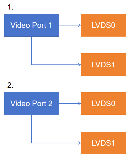
The following example shows the output using VP1, that is, Method 1 in the figure:
&lvds0_in_vp1 {
   status = "okay";
};


&lvds1_in_vp1 {
   status = "okay";
};

&lvds1_in_vp2 {
   status = "disabled";
};
3. Specify the output order of the LVDS channels:
panel {
   /* ... Relevant panel parameters are filled in here */


   ports {
      #address-cells = <1>;
      #size-cells = <0>;
      port@0 {
         reg = <0>;
         dual-lvds-odd-pixels; /* Output odd pixels */
         panel_in_lvds0: endpoint {
           remote-endpoint = <&lvds0_out_panel>;
         };
      };
      port@1 {
         reg = <1>;
         dual-lvds-even-pixels; /* Output even pixels */

         panel_in_lvds1: endpoint {
           remote-endpoint = <&lvds1_out_panel>;
         };
      };
   };
};
In this example, LVDS0 outputs dual-lvds-odd-pixels , that is, odd pixels; LVDS1 outputs dual-lvds-even-pixels , that is, even pixels. In practice, the order of the them can be swapped as needed.
5.3 Dual LVDS (Dual-channel LVDS) Configuration Applicable to RK3288
This section is applicable to RK3288.
1. Add the dual-channel attribute to the lvds node to indicate that Dual LVDS is used.
&lvds {
   status = "okay";
   dual-channel;


   ports {
      port@1 {
         reg = <1>;
         lvds0_out_panel: endpoint {
           remote-endpoint = <&panel_in_lvds0>;
         };
      };
   };
};
2. Specify on which VOP the LVDS is output, which can be vopb or vopl.
/* Output on vopb */
&lvds_in_vopb {

   status = "okay";
};

/* Or, output on vopl */
&lvds_in_vopl {
   status = "okay";
}
3. Specify the output order of the LVDS channels. For RK3288, the rockchip,data-swap attribute can be added to the lvds node to swap the output order:
&lvds {
   rockchip,data-swap;

};
5.4 Configuration for Two VPs Each Connected to an Independent Single-channel LVDS Panel
In this case, only need to configure each single-channel LVDS according to the single-channel LVDS configuration.
For this case, do not set the dual-channel attribute, otherwise it will be recognized as Dual LVDS
In practical use, the allocation method of the Video Port needs to be specified. There are 2 possible allocation methods, as shown in the following figure:
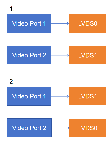
The following DTS examples respectively correspond to Method 1 and Method 2 in the figure:
/*
 * VP1 -> LVDS0, VP2 -> LVDS1

 */
&lvds0_in_vp1 {
   status = "okay";
};

&lvds1_in_vp2 {
   status = "okay";
};

/*
 * Or, VP2 -> LVDS0, VP1 -> LVDS1
 */
&lvds0_in_vp2 {

   status = "okay";
};

&lvds1_in_vp1 {
   status = "okay";
};
5.5 Configuration for One VP Connected to Two Single-channel LVDS Panels
In this scenario, one VP is connected to two single-channel LVDS panels, and each panel shows half of the content in the VP.
It is worth noting that in this case, it is currently implemented as an extension of Dual LVDS. Therefore, its configuration method is similar to that of Dual LVDS:
1. Add the dual-channel attribute to the lvds node of LVDS0.
&lvds0 {
   status = "okay";
   dual-channel;


   ports {
      port@1 {
         reg = <1>;
         lvds0_out_panel: endpoint {
           remote-endpoint = <&panel_in_lvds0>;
         };
      };
   };
};
2. Specify the allocation method of the Video Port. For the scenario of one VP connected to two single- channel LVDS panels on RK356X, it can be selected to output on either VP1 or VP2. The possible allocation methods are shown in the following figure.
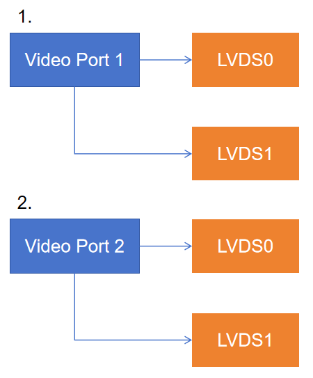
The following example shows the output using VP1, that is, Method 1 in the figure:
&lvds0_in_vp1 {
   status = "okay";

};

&lvds1_in_vp1 {
   status = "okay";
};

&lvds1_in_vp2 {
   status = "disabled";
};
3. Specify the output order of the LVDS channels:
panel {
   /*... Relevant panel parameters are filled in here */


   ports {
      #address-cells = <1>;
      #size-cells = <0>;
      port@0 {
         reg = <0>;
         dual-lvds-left-pixels; /* Output the left-half content */
         panel_in_lvds0: endpoint {

           remote-endpoint = <&lvds0_out_panel>;
         };
      };
      port@1 {
         reg = <1>;
         dual-lvds-right-pixels; /* Output the right-half content */
         panel_in_lvds1: endpoint {
           remote-endpoint = <&lvds1_out_panel>;
         };
      };
   };
};
In the current implementation, we have additionally defined the dual-lvds-left-pixels and dual-lvds-right-pixels attributes to distinguish the output order. It can be changed as needed in practical use.
5.6 Configuration for One VP Connected to Two Single-channel LVDS panels (Connector Mirror)
In this scenario, one VP is connected to two single-channel LVDS panels, and each panel has the same timing parameters and displays exactly the same content.
For the configuration of each panel’s timing, it can refer to the single-channel LVDS configuration.
In terms of the allocation method of the Video Port and LVDS, it can be specified to output from either VP1 or VP2:
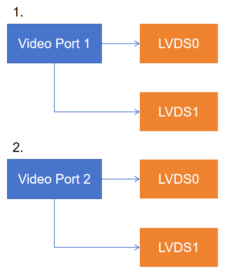
/* Output using VP1 */
&lvds0_in_vp1 {
   status = "okay";

};

&lvds1_in_vp1 {
   status = "okay";
};

/* Or, output using VP2 */
&lvds0_in_vp2 {
   status = "okay";
};

&lvds1_in_vp2 {

   status = "okay";
};
6. LVDS Debugging Method
With the help of the summary node of VOP, the current LVDS Connector information can be viewed:
cat /sys/kernel/debug/dri/0/summary
When Dual LVDS is enabled and the driver has been successfully loaded, the Connector node named LVDS-DUAL will be displayed:
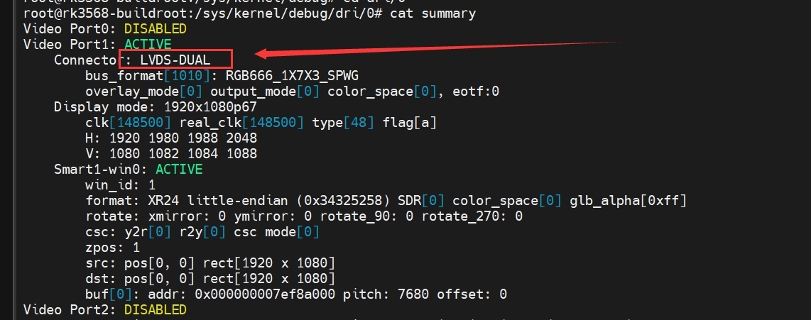
Note that for the scenario where one VP is connected to two single-channel LVDS panels and each panel displays half of the content in the VP, it will also be displayed as LVDS-DUAL.
When two single-channel LVDS panels are used, different LVDS Connector nodes can be seen:
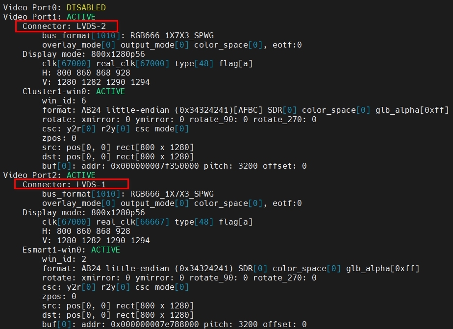
At this time, which VP the LVDS Connector is allocated to depends on the specific configuration.
7. FAQ
7.1 No Output on LVDS1 Channel
First, check the output information of VOP summary to ensure that LVDS1 has been correctly enabled. If there is still no output, try to update the Loader.
7.2 Blurred/Jagged Content Output by Dual LVDS
It is possible that the outputs of LVDS0 and LVDS1 are reversed. You can try to swap the positions of the dual-lvds-odd-pixels and dual-lvds-even-pixels attributes in the DTS configuration.
7.3 Display content is Black/White
Check the hardware connection and whether the outputs of the backlight pin and the Enable pin are correct.
7.4 Modify LVDS Common-mode/Differential-mode Voltage
For RK356X, modify the DTS attributes corresponding to the PHY:
Among them, inno,lvds-vcom is the common-mode voltage, and inno,lvds-vod is the differential-mode voltage.
The common-mode voltages of RK356X are as follows:
1000 mV
950 mV (default value)
900 mV
850 mV
The differential-mode voltages of RK356X are as follows:
400 mV
350 mV (default value)
300 mV
250 mV
&video_phy0 {
      inno,lvds-vcom = <1000>; /* 1000mV */
      inno,lvds-vod = <400>; /* 400mV */

};