
This is a Rockchip platform reference. The source product scope is RK3576 / Linux Kernel 6.1 and RK3588 / Linux Kernel 5.10 or 6.1. For an ArmSoM project, verify each board’s SoC, exposed DP/Type-C interfaces, PD controller, PHY wiring, SDK/BSP patches and kernel configuration. This does not imply that every ArmSoM board supports every described mode. No ArmSoM hardware testing was performed; logs, display photographs and performance values are source examples or capability statements.
Sources: the Chinese Rockchip DisplayPort guide (cover V1.3.0, revision table V1.3.3) and English V1.2.1. As explicitly approved, the newer Chinese body is the common baseline. In particular, the detailed SST/MST node/configuration sections §2.1–2.4, dclk source §2.9 and DP Status §3.10 are translated from the newer Chinese source, not presented as existing in the older English edition. Chinese uses its 17 original figures; English and Russian use the 17 corresponding English-PDF originals. No additional standalone figure was found for the new explanations. Code and commands follow the newer Chinese source, with original comments retained.
Editorial notes · ArmSoM documentation · Rockchip
1. Introduction to Rockchip DisplayPort
1.1 Features
The capabilities of the Rockchip RK3576 and RK3588 DP interfaces are listed below:
| Function | RK3576 | RK3588 |
|---|---|---|
| Version | 1.4a | 1.4a |
| SST | Supported | Supported |
| MST | Supported | Not supported |
| DSC | Not supported | Not supported |
| Maximum resolution | 4K@120Hz | 8K@30Hz |
| Main-Link lanes | 1/2/4 lanes | 1/2/4 lanes |
| Main-Link rate | 8.1/5.4/2.7/1.62 Gbps/lane | 8.1/5.4/2.7/1.62 Gbps/lane |
| AUX_CH | 1 M | 1 M |
| Color format | RGB/YUV444/YUV422/YUV420 | RGB/YUV444/YUV422/YUV420 |
| Color depth | 8/10 bit (6bit only for RGB) | 8/10 bit (6bit only for RGB) |
| Display split mode | Supported | Supported |
| HDCP | HDCP2.2/HDCP1.3 | HDCP2.2/HDCP1.3 |
| Type-C support | DP Alternate Mode | DP Alternate Mode |
| I2S | Supported | Supported |
| SPDIF | Supported | Supported |
| HDR | Supported | Supported |
| DP Dual Mode(DP++) | Not supported | Not supported |
Note:
- The source states that RK3576 and RK3528 are backward compatible with DP1.2.
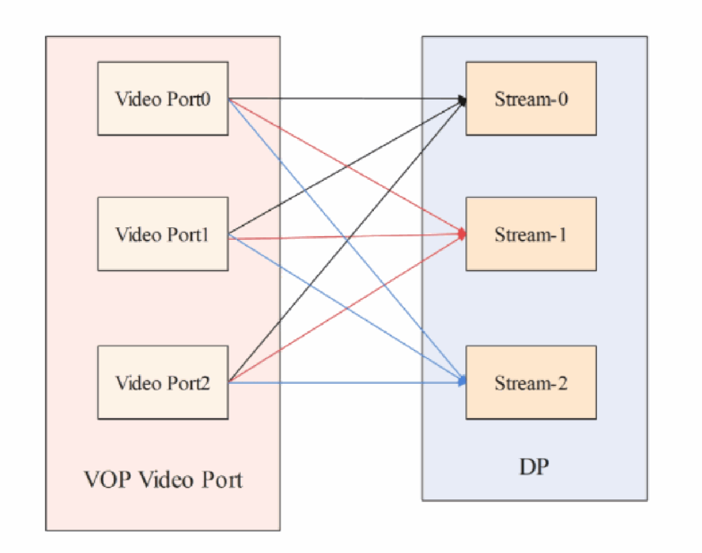
RK3576 has only one physical DP interface, but internally accepts three display streams in MST mode. These are called Stream-0, Stream-1 and Stream-2 to distinguish them from physical interfaces. The maximum capabilities of each stream are:
| DP Stream Channel | Maximum width | Maximum height | Maximum pixel clock |
|---|---|---|---|
| Stream-0 | 4096 | 4096 | 1188MHz |
| Stream-1 | 2560 | 2560 | 300MHz |
| Stream-2 | 1920 | 1920 | 150MHz |
1.2 Connections between DP and VOP
RK3576 has three VOP Video Ports and one DP controller. In MST mode the DP controller can receive up to three display streams from VOP. Each of Stream-0/1/2 can receive data from Video Port0/1/2. SST mode uses only Stream-0; MST mode can use Stream-0/1/2.
RK3588 has four VOP Video Ports and two DP controllers. Only Video Port 0/1/2 can output to DP0/1, as shown below.
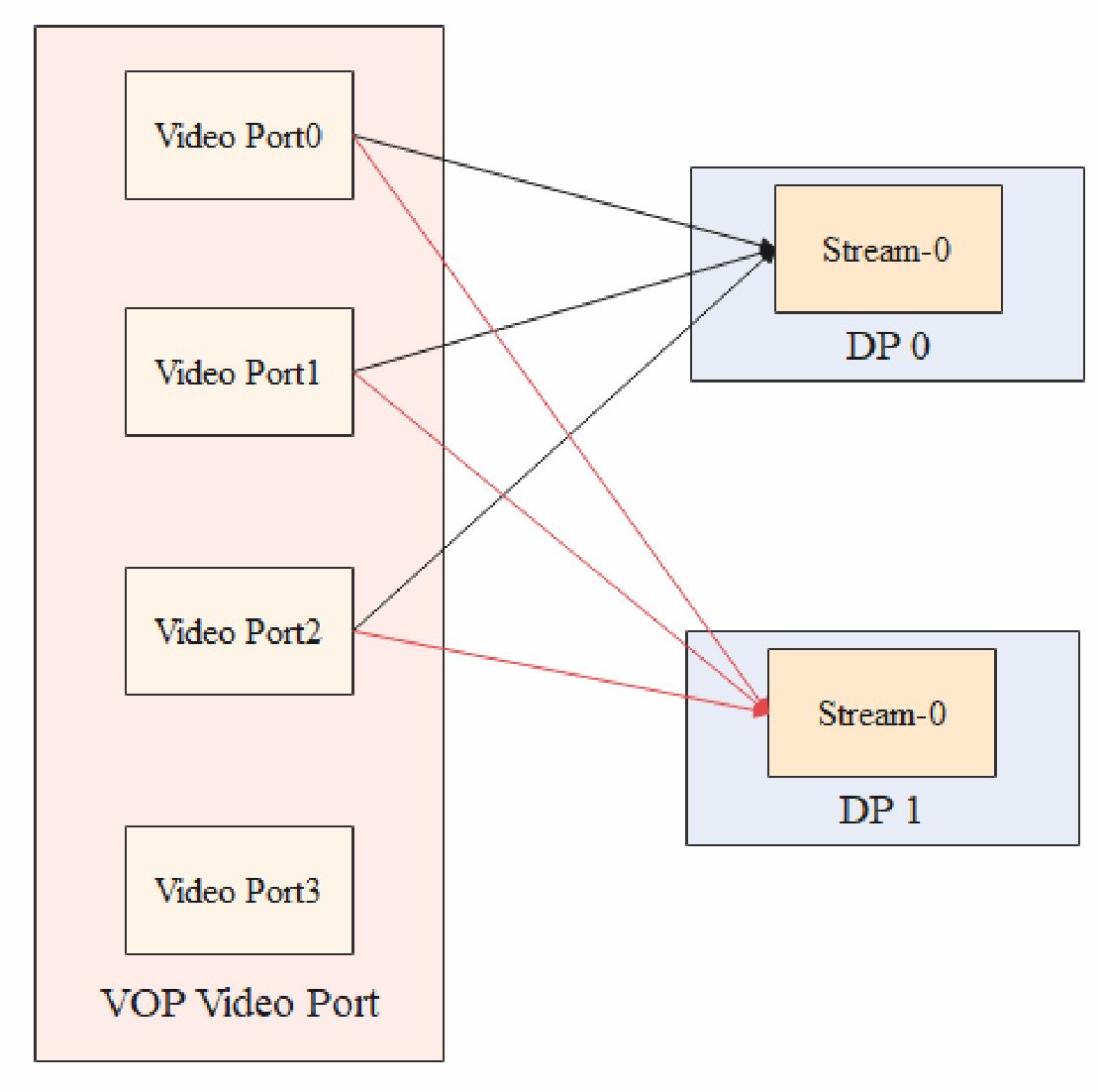
The two RK3588 DP interfaces do not support MST and internally accept only Stream-0. On platforms without MST, a Video Port therefore outputs to the DP interface’s Stream-0 by default.
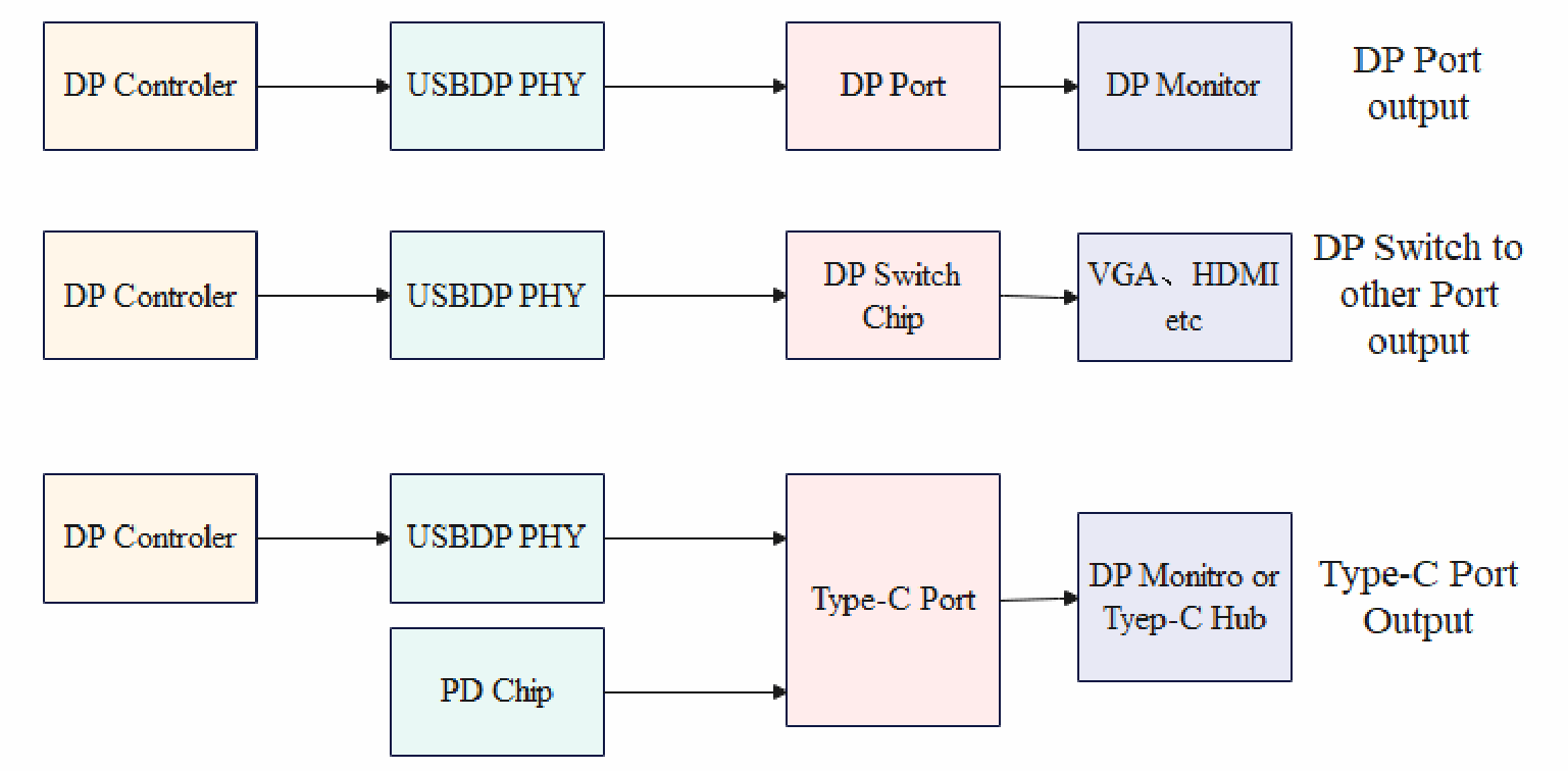
1.3 DP output
Depending on the application, DP output can use a Type-C connector, a standard DP connector, or another bridge/converter chip.
In MST mode RK3576 can connect up to three monitors, using a daisy chain of MST monitors:
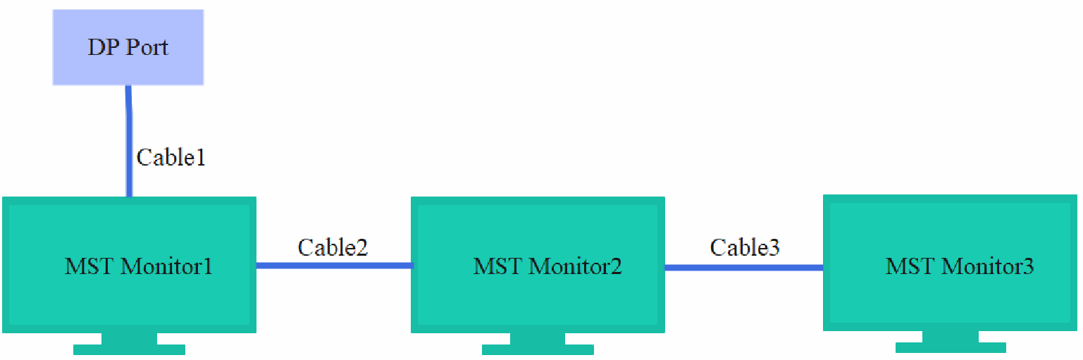
Only the last monitor in the daisy chain may be an SST monitor; all preceding monitors must support MST.
Alternatively, connect through an MST HUB:
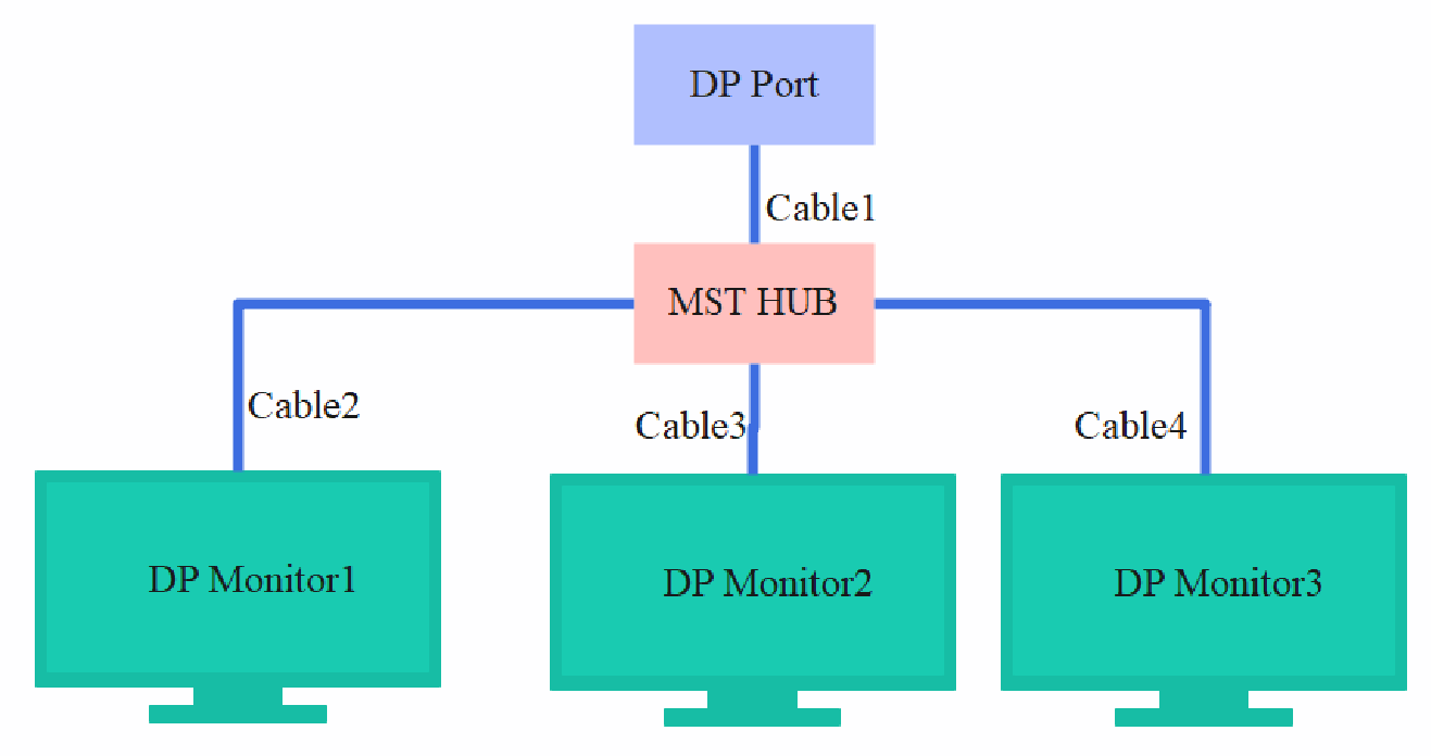
When an MST HUB is used, the connected DP monitors may be either SST or MST monitors.
1.4 Source code paths
U-Boot driver code:
drivers/video/drm/dw-dp.c
drivers/phy/phy-rockchip-usbdp.c
Kernel driver code:
drivers/gpu/drm/rockchip/dw-dp.c
drivers/phy/rockchip/phy-rockchip-usbdp.c
RK3576 reference DTS configuration:
arch/arm64/boot/dts/rockchip/rk3576-evb1.dtsi
arch/arm64/boot/dts/rockchip/rk3576-test2.dtsi
RK3588 reference DTS configuration:
arch/arm64/boot/dts/rockchip/rk3588-evb1-lp4.dtsi
arch/arm64/boot/dts/rockchip/rk3588-evb2-lp4.dtsi

arch/arm64/boot/dts/rockchip/rk3588-evb3-lp5.dtsi
arch/arm64/boot/dts/rockchip/rk3588-nvr-demo.dtsi
1.5 Driver loading
The following log indicates whether the driver has finished loading:
RK3576:
 [1.991964] rockchip-drm display-subsystem: bound 27e40000.dp (ops 0xffffffc0094a1570) //DP
驱动加载完成

RK3588:
 [2.472282] rockchip-drm display-subsystem: bound fde50000.dp (ops dw_dp_component_ops)
//DP0 驱动加载完成
 [2.472319] rockchip-drm display-subsystem: bound fde60000.dp (ops dw_dp_component_ops)
//DP1 驱动加载完成
2. Functional configuration
The basic DTS node structure differs between DP platforms that support MST and platforms that support only SST.
2.1 SST node configuration
On SST-only platforms such as RK3588, one DP controller supports only one DP output. A single ports child node is sufficient to describe the display paths available to that output:
dp0: dp@fde50000 {
   compatible = "rockchip,rk3588-dp";

   ...

   ports {
      #address-cells = <1>;
      #size-cells = <0>;

      port@0 {
         reg = <0>;
         #address-cells = <1>;
         #size-cells = <0>;
         dp0_in_vp0: endpoint@0 {
           reg = <0>;

           remote-endpoint = <&vp0_out_dp0>;
           status = "disabled";
         };

         dp0_in_vp1: endpoint@1 {
           reg = <1>;
           remote-endpoint = <&vp1_out_dp0>;
           status = "disabled";
         };

         dp0_in_vp2: endpoint@2 {
           reg = <2>;

           remote-endpoint = <&vp2_out_dp0>;
           status = "disabled";
         };
      };
   ...
   };
};
2.2 MST node configuration
On MST-capable platforms such as RK3576, one DP controller supports three display streams. A single ports node cannot describe the paths of multiple DP channels, so multiple child nodes are required:
dp: dp@27e40000 {
   compatible = "rockchip,rk3576-dp";

   ...
   dp0: dp0 {
      status = "disabled";

      ports {
         #address-cells = <1>;
         #size-cells = <0>;

         port@0 {
           reg = <0>;
           #address-cells = <1>;
           #size-cells = <0>;


           dp0_in_vp0: endpoint@0 {
              reg = <0>;
              remote-endpoint = <&vp0_out_dp0>;
              status = "disabled";
           };

           dp0_in_vp1: endpoint@1 {
              reg = <1>;
            remote-endpoint = <&vp1_out_dp0>;
            status = "disabled";
         };


         dp0_in_vp2: endpoint@2 {
            reg = <2>;
            remote-endpoint = <&vp2_out_dp0>;
            status = "disabled";
         };
      };
   };
};

dp1: dp1 {
   status = "disabled";


   ports {
      #address-cells = <1>;
      #size-cells = <0>;

      port@0 {
         reg = <0>;
         #address-cells = <1>;
         #size-cells = <0>;

         dp1_in_vp0: endpoint@0 {
            reg = <0>;
            remote-endpoint = <&vp0_out_dp1>;

            status = "disabled";
         };

         dp1_in_vp1: endpoint@1 {
            reg = <1>;
            remote-endpoint = <&vp1_out_dp1>;
            status = "disabled";
         };

         dp1_in_vp2: endpoint@2 {
            reg = <2>;
            remote-endpoint = <&vp2_out_dp1>;

            status = "disabled";
         };
      };
   };
};

dp2: dp2 {
   status = "disabled";

   ports {
      #address-cells = <1>;
      #size-cells = <0>;
      port@0 {
           reg = <0>;
           #address-cells = <1>;
           #size-cells = <0>;


           dp2_in_vp0: endpoint@0 {
              reg = <0>;
              remote-endpoint = <&vp0_out_dp2>;
              status = "disabled";
           };

           dp2_in_vp1: endpoint@1 {
              reg = <1>;
              remote-endpoint = <&vp1_out_dp2>;
              status = "disabled";
           };


           dp2_in_vp2: endpoint@2 {
              reg = <2>;
              remote-endpoint = <&vp2_out_dp2>;
              status = "disabled";
           };
         };
      };
   };
};
The dp0/1/2 child nodes describe the display paths supported by Stream-0/1/2 respectively.
Compared with SST-only DTS configuration, an MST platform has an extra level of DP-channel child nodes.
2.3 Enabling DP
DP and USB3.0 share a PHY. PHY lane configuration depends on whether the output is Type-C or non-Type-C.
2.3.1 DP Alt Mode (Type-C)
DisplayPort Alt Mode communicates with the monitor through the PD (Power Delivery) state machine to map lanes and convey HPD information. The following diagram shows entering DP Mode through PD and transferring HPD information with attention commands.
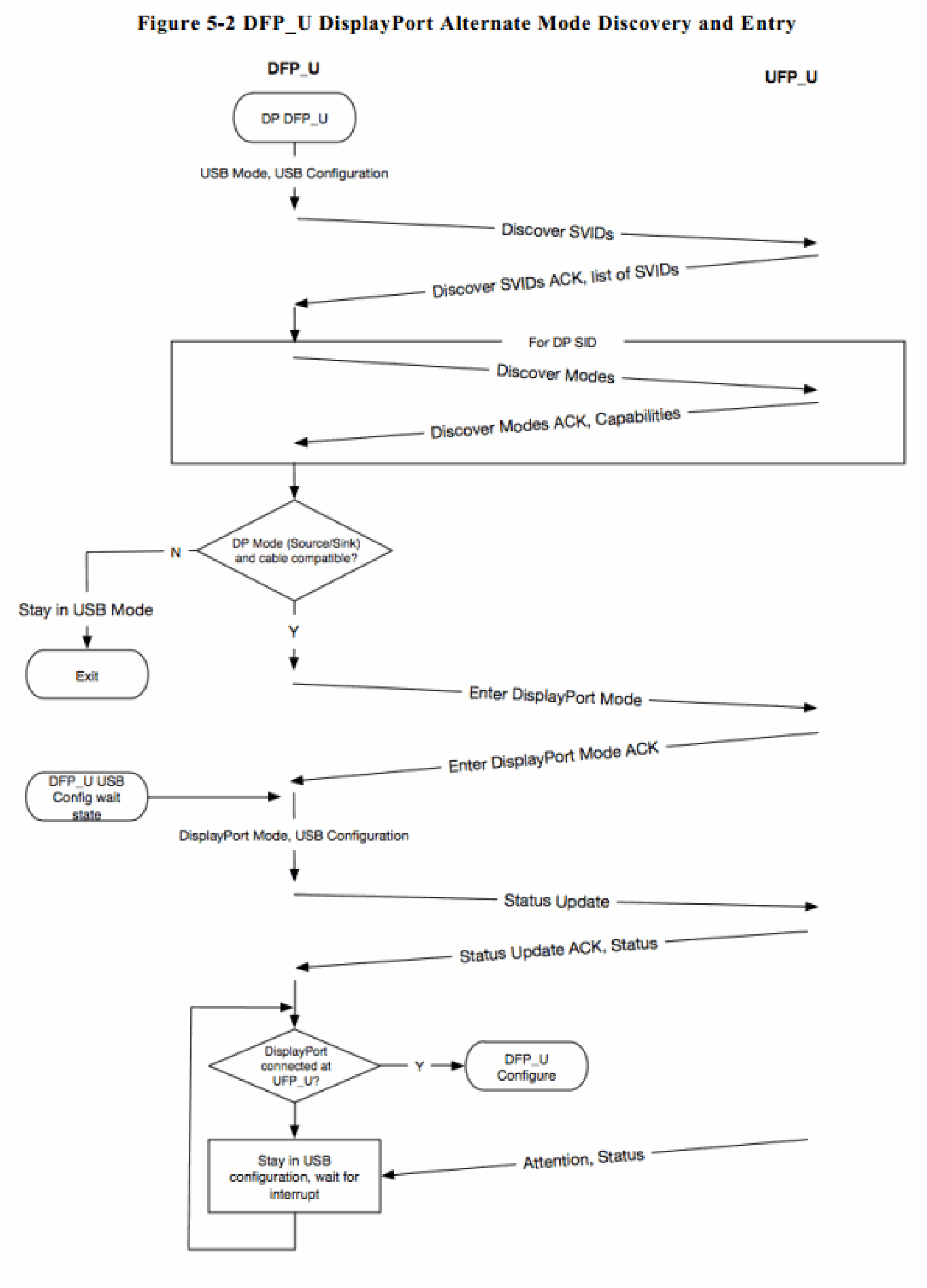
2.3.1.1 SST controller configuration
For SST-only platforms such as RK3588:
&dp0 {
   status = "okay";
};


&dp0_in_vp2 {
   status = "okay";
};
This example enables DP0 and binds it to VOP Video Port2. It is only a reference configuration. In an actual design, enable DP0 or DP1 as needed and bind it to the required Video Port (0/1/2).
2.3.1.2 MST controller configuration
For MST-capable platforms such as RK3576:
&dp {
   status = "okay";
};


&dp0 {
   status = "okay";
};

&dp0_in_vp2 {
   status = "okay";
};
An MST-capable platform must enable the DP device node, the desired DP Stream channel, and the VOP Video Port bound to that channel. This example enables Stream-0 and binds it to VOP Video Port2.
On MST-capable platforms, SST mode always uses DP Stream-0. Therefore dp0 must be enabled; configure dp1 and dp2 according to actual use.
2.3.1.3 PHY configuration
PHY configuration is the same for platforms with and without MST. The following example uses RK3588 usbdp phy0:
&usbdp_phy0 {
   status = "okay";

   orientation-switch;
   /* DP related config */
   svid = <0xff01>;
   sbu1-dc-gpios = <&gpio4 RK_PA6 GPIO_ACTIVE_HIGH>;
   sbu2-dc-gpios = <&gpio4 RK_PA7 GPIO_ACTIVE_HIGH>;
   /* DP related config */

   port {
      #address-cells = <1>;
      #size-cells = <0>;
      usbdp_phy0_orientation_switch: endpoint@0 {
         reg = <0>;
         remote-endpoint = <&usbc0_orien_sw>;

      };

      /* DP related config */
      usbdp_phy0_dp_altmode_mux: endpoint@1 {
         reg = <1>;
         remote-endpoint = <&dp_altmode_mux>;
      };
      /* DP related config */
   };
};
sbu1-dc-gpios and sbu2-dc-gpios:
Type-C SBU1 and SBU2 are multiplexed with DP AUX_CH. In normal orientation AUX_CH_P uses SBU1 and AUX_CH_N uses SBU2 (the source spells this SUB2). In reverse orientation AUX_CH_P uses SBU2 and AUX_CH_N uses SBU1. DP requires AUX_CH_P to be pulled down and AUX_CH_N to be pulled up. The mapping changes with connector orientation. Rockchip uses two GPIOs to control the pull-up/pull-down states of SBU1 and SBU2: sbu1-dc-gpios and sbu2-dc-gpios in DTS. Configure these GPIOs according to the schematic, such as TYPEC0_SBU1_DC and TYPEC0_SBU2_DC shown below. The PHY driver adjusts their output levels to match the current orientation.
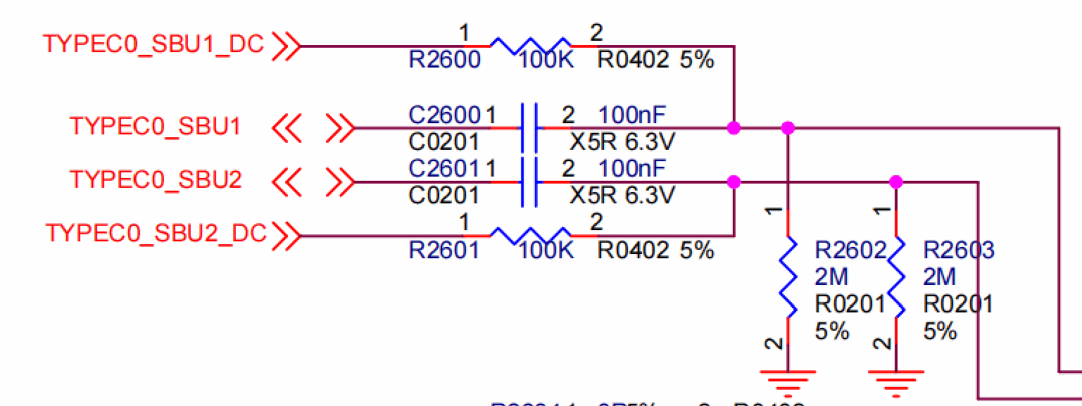
svid:
For DP, the fixed value is 0xff01.
2.3.1.4 PD-controller configuration
Type-C configures lanes and HPD state through CC detection and PD negotiation. Configure the PD controller as well:
&i2c2 {
   status = "okay";


   usbc0: fusb302@22 {
      compatible = "fcs,fusb302";
      reg = <0x22>;
interrupt-parent = <&gpio3>;
interrupts = <RK_PB4 IRQ_TYPE_LEVEL_LOW>;
pinctrl-names = "default";

pinctrl-0 = <&usbc0_int>;
vbus-supply = <&vbus5v0_typec>;
status = "okay";

ports {
   #address-cells = <1>;
   #size-cells = <0>;

   port@0 {
      reg = <0>;
      usbc0_role_sw: endpoint@0 {
         remote-endpoint = <&dwc3_0_role_switch>;

      };
   };
};

usb_con: connector {
   compatible = "usb-c-connector";
   label = "USB-C";
   data-role = "dual";
   power-role = "dual";
   try-power-role = "sink";
   op-sink-microwatt = <1000000>;
   sink-pdos =
      <PDO_FIXED(5000, 1000, PDO_FIXED_USB_COMM)>;

   source-pdos =
      <PDO_FIXED(5000, 3000, PDO_FIXED_USB_COMM)>;

   /* DP related config */
   altmodes {
      #address-cells = <1>;
      #size-cells = <0>;

      altmode@0 {
         reg = <0>;
         svid = <0xff01>;
         vdo = <0xffffffff>;

      };
   };
   /* DP related config */

   ports {
      #address-cells = <1>;
      #size-cells = <0>;

      port@0 {
         reg = <0>;
         usbc0_orien_sw: endpoint {
            remote-endpoint = <&usbdp_phy0_orientation_switch>;
         };
           };

           /* DP related config */

           port@1 {
              reg = <1>;
              dp_altmode_mux: endpoint {
                 remote-endpoint = <&usbdp_phy0_dp_altmode_mux>;
              };
           };
           /* DP related config */
         };
      };
   };
};
In altmode@0, svid is fixed at 0xff01 and vdo at 0xffffffff.
The source lists fusb302 and hub311 as supported PD chips. Their drivers are /drivers/usb/typec/tcpm/fusb302.c and /drivers/usb/typec/tcpm/tcpci_husb311.c respectively.
2.3.2 DP Legacy Mode
For non-Type-C output, whether through a standard DP connector or another converter, the configuration procedure is essentially the same and requires an HPD pin. Use either the dedicated DP_HPD pin with its IOMUX configuration or an ordinary GPIO for detection.
2.3.2.1 HPD configuration in SST mode
For platforms without MST such as RK3588, configure the dedicated DP_HPD pin as follows:
&dp1 {
   pinctrl-0 = <&dp1m2_pins>;
   pinctrl-names = "default";

   status = "okay";
};

&dp1_in_vp2 {
   status = "okay";
};
To use an ordinary GPIO for HPD detection:
&dp1 {
   pinctrl-names = "default";

   pinctrl-0 = <&dp1_hpd>;
   hpd-gpios = <&gpio1 RK_PB5 GPIO_ACTIVE_HIGH>;
   status = "okay";
};
&dp1_in_vp2 {
   status = "okay";
};


&pinctrl {
   dp {
      dp1_hpd: dp1-hpd {
         rockchip,pins = <1 RK_PB5 RK_FUNC_GPIO &pcfg_pull_down>;
      };
   };
};
2.3.2.2 HPD configuration in MST mode
For MST-capable platforms such as RK3576, configure the dedicated DP_HPD pin as follows:
&dp {
   pinctrl-0 = <&dp1m2_pins>;
   pinctrl-names = "default";

   status = "okay";
};

&dp0 {
   status = "okay";
};

&dp0_in_vp2 {
   status = "okay";
};
To use an ordinary GPIO for HPD detection:
&dp {
   pinctrl-names = "default";
   pinctrl-0 = <&dp_hpd>;

   hpd-gpios = <&gpio1 RK_PB5 GPIO_ACTIVE_HIGH>;
   status = "okay";
};

&dp0 {
   status = "okay";
};

&dp0_in_vp2 {
   status = "okay";
};


&pinctrl {
   dp {
      dp_hpd: dp-hpd {
         rockchip,pins = <1 RK_PB5 RK_FUNC_GPIO &pcfg_pull_down>;
      };
   };
};
In both configurations, HPD belongs to the entire DP interface and is configured on the device node.
2.3.2.3 PHY configuration
DP and USB 3.0 share a PHY. With non-Type-C DP output, DTS must specify which PHY lanes are assigned to DP and their order. DP can use two or four PHY lanes.
Physical PHY lane numbers correspond to pins as follows:
| Pin name | SSRX1 | SSTX1 | SSRX2 | SSTX2 |
|---|---|---|---|---|
| PHY lane | 0 | 1 | 2 | 3 |
For four DP lanes, use the following DTS property:
rockchip,dp-lane-mux = <x x x x>;
For two DP lanes, use:
rockchip,dp-lane-mux = <x x>;
The index denotes the DP lane and the value denotes the PHY lane.
For either two- or four-lane hardware, the design normally uses OPTION1 or OPTION2 below.
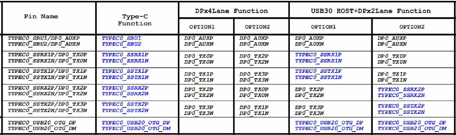
Editable transcription of the pin-mapping table above:
| Pin name | Type-C function | DP x4 Lane OPTION1 | DP x4 Lane OPTION2 | USB30 HOST + DP x2 Lane OPTION1 | USB30 HOST + DP x2 Lane OPTION2 |
|---|---|---|---|---|---|
| TYPEC0_SBU1/DP0_AUXP | TYPEC0_SBU1 | DP0_AUXP | DP0_AUXP | DP0_AUXP | DP0_AUXP |
| TYPEC0_SBU2/DP0_AUXN | TYPEC0_SBU2 | DP0_AUXN | DP0_AUXN | DP0_AUXN | DP0_AUXN |
| TYPEC0_SSRX1P/DP0_TX0P | TYPEC0_SSRX1P | DP0_TX0P | DP0_TX2P | TYPEC0_SSRX1P | DP0_TX0P |
| TYPEC0_SSRX1N/DP0_TX0N | TYPEC0_SSRX1N | DP0_TX0N | DP0_TX2N | TYPEC0_SSRX1N | DP0_TX0N |
| TYPEC0_SSTX1P/DP0_TX1P | TYPEC0_SSTX1P | DP0_TX1P | DP0_TX3P | TYPEC0_SSTX1P | DP0_TX1P |
| TYPEC0_SSTX1N/DP0_TX1N | TYPEC0_SSTX1N | DP0_TX1N | DP0_TX3N | TYPEC0_SSTX1N | DP0_TX1N |
| TYPEC0_SSRX2P/DP0_TX2P | TYPEC0_SSRX2P | DP0_TX2P | DP0_TX0P | DP0_TX2P | TYPEC0_SSRX2P |
| TYPEC0_SSRX2N/DP0_TX2N | TYPEC0_SSRX2N | DP0_TX2N | DP0_TX0N | DP0_TX2N | TYPEC0_SSRX2N |
| TYPEC0_SSTX2P/DP0_TX3P | TYPEC0_SSTX2P | DP0_TX3P | DP0_TX1P | DP0_TX3P | TYPEC0_SSTX2P |
| TYPEC0_SSTX2N/DP0_TX3N | TYPEC0_SSTX2N | DP0_TX3N | DP0_TX1N | DP0_TX3N | TYPEC0_SSTX2N |
| TYPEC0_USB20_OTG_DP | TYPEC0_USB20_OTG_DP | TYPEC0_USB20_OTG_DP | TYPEC0_USB20_OTG_DP | ||
| TYPEC0_USB20_OTG_DM | TYPEC0_USB20_OTG_DM | TYPEC0_USB20_OTG_DM | TYPEC0_USB20_OTG_DM |
Four-lane DP, OPTION1 mapping:
| DP lane | PHY lane | Pin name |
|---|---|---|
| 0 | 0 | SSRX1 |
| 1 | 1 | SSTX1 |
| 2 | 2 | SSRX2 |
| 3 | 3 | SSTX2 |
DP lane denotes the DP lane number.
DTS configuration:
&usbdp_phy1 {
   rockchip,dp-lane-mux = <0 1 2 3>;
   status = "okay";

};
Four-lane DP, OPTION2 mapping:
| DP lane | PHY lane | Pin name |
|---|---|---|
| 0 | 2 | SSRX2 |
| 1 | 3 | SSTX2 |
| 2 | 0 | SSRX1 |
| 3 | 1 | SSTX1 |
DP lane denotes the DP lane number.
DTS configuration:
&usbdp_phy1 {
   rockchip,dp-lane-mux = <2 3 0 1>;
   status = "okay";

};
Two-lane DP, OPTION1 mapping:
| DP lane | PHY lane | Pin name |
|---|---|---|
| 0 | 2 | SSRX2 |
| 1 | 3 | SSTX2 |
Two-lane DP configuration:
&usbdp_phy1 {
   rockchip,dp-lane-mux = <2 3>;
   status = "okay";

};
Two-lane DP, OPTION2 mapping:
| DP lane | PHY lane | Pin name |
|---|---|---|
| 0 | 0 | SSRX1 |
| 1 | 1 | SSTX1 |
Two-lane DP configuration:
&usbdp_phy1 {
   rockchip,dp-lane-mux = <0 1>;
   status = "okay";

};
2.4 Connecting a panel to DP
When DP connects to an eDP panel, eDP-specific features such as PSR, Multi-SST and ALPM are not supported. Use the following panel configuration as a reference and adapt it to the actual hardware.
2.4.1 Panel configuration in SST mode
Configuration for SST-only platforms such as RK3588:
/ {
   ...
   panel-edp {

      compatible = "simple-panel";
      backlight = <&backlight>;
      power-supply = <&vcc3v3_lcd_edp>;
      prepare-delay-ms = <120>;
      enable-delay-ms = <120>;
      unprepare-delay-ms = <120>;
      disable-delay-ms = <120>;
      width-mm = <120>;
      height-mm = <160>;

      panel-timing {
         clock-frequency = <200000000>;
         hactive = <1536>;

         vactive = <2048>;
         hfront-porch = <12>;
         hsync-len = <16>;
         hback-porch = <48>;
         vfront-porch = <8>;
         vsync-len = <4>;
         vback-porch = <8>;
         hsync-active = <0>;
         vsync-active = <0>;
         de-active = <0>;
         pixelclk-active = <0>;
      };


      port {
         panel_in_edp: endpoint {
           remote-endpoint = <&dp0_out>;
         };
      };
   };
   ...

};

&dp0 {
   force-hpd;
   status = "okay";
};

&dp0_in_vp2 {
   status = "okay";
};

&dp0_out {

   remote-endpoint = <&panel_in_edp>;
};

&usbdp_phy0 {
   rockchip,dp-lane-mux = <0 1 2 3>;
   status = "okay";
};
2.4.2 Panel configuration on MST-capable platforms
Reference configuration for MST-capable platforms such as RK3576:
/ {
   ...

   panel-edp {
      compatible = "simple-panel";
      backlight = <&backlight>;
      power-supply = <&vcc3v3_lcd_edp>;
      prepare-delay-ms = <120>;
      enable-delay-ms = <120>;
      unprepare-delay-ms = <120>;
      disable-delay-ms = <120>;
      width-mm = <120>;
      height-mm = <160>;

      panel-timing {
         clock-frequency = <200000000>;

         hactive = <1536>;
         vactive = <2048>;
         hfront-porch = <12>;
         hsync-len = <16>;
         hback-porch = <48>;
         vfront-porch = <8>;
         vsync-len = <4>;
         vback-porch = <8>;
         hsync-active = <0>;
         vsync-active = <0>;
         de-active = <0>;
         pixelclk-active = <0>;

      };

      port {
         panel_in_edp: endpoint {
           remote-endpoint = <&dp0_out_panel>;
         };
      };
   };
   ...
};

&dp {

   force-hpd;
   status = "okay";
};

&dp0 {
   status = "okay";

   ports {
      port@1 {
         reg = <1>;

         dp0_out_panel: endpoint {
           remote-endpoint = <&panel_in_edp>;

         };
      };
   };
};

&dp0_in_vp2 {
   status = "okay";
};

&usbdp_phy {
   rockchip,dp-lane-mux = <0 1 2 3>;
   status = "okay";

};
In both SST and MST configurations, force-hpd describes HPD for the entire DP interface and belongs on the device node. Display-path configuration is specific to the DP stream; MST platforms must modify the corresponding child node.
On MST-capable platforms, connecting a panel currently supports only SST mode. Consequently the display path must use Stream-0, represented by dp0.
The source describes force-hpd on dp0 as making the driver treat the eDP panel as always connected. This property is optional: check whether the panel exposes HPD and whether HPD assertion and AUX access have ordering requirements. If AUX access must follow HPD assertion, do not configure force-hpd: otherwise AUX may be accessed before HPD is high and fail. If an HPD pin is needed, follow the DP Legacy Mode HPD configuration above (the source’s section reference ‘1.2.1’ is stale).
panel-timing specifies the supported timing. Configure it if the panel has no EDID or the timing read from EDID is inaccurate. Otherwise timing can be obtained directly from EDID.
Configure power sequencing and backlight according to the panel and board design.
2.5 DP boot logo
With boot-logo support configured, a monitor attached before power-on can display the logo during U-Boot. Otherwise the application image becomes visible only after the system starts. Add the following configuration:
&route_dp0 {
   status = "okay";

   connect = <&vp2_out_dp0>;
};
Here the connect property binds DP to VOP Port2 during U-Boot. The DTSI configuration must therefore permit that binding:
&dp0_in_vp2 {
   status = "okay";
};
Notes:
-
The source does not support a DP boot logo over Type-C.
-
On MST-capable platforms, the boot logo is supported only in SST mode.
2.6 DP connector-split mode
In connector-split mode, an image is divided into equal left and right halves, transmitted through DP0 and DP1 respectively. In this diagram DP0 is the left half and DP1 the right half.
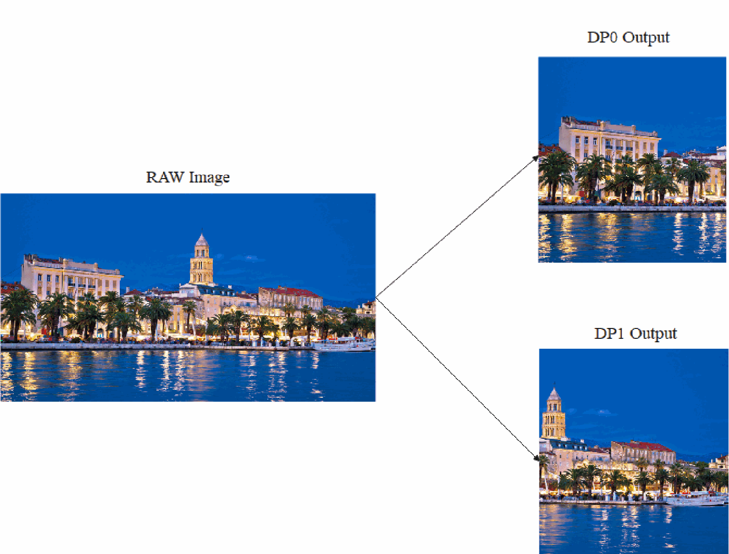
Configuration:
&dp0 {
   split-mode;
   status = "okay";

};

&dp0_in_vp2 {
   status = "okay";
};

&dp1 {
   status = "okay";
};
Add split-mode to the left-half DP node and bind it to the output Video Port. In this example DP0 is left and DP1 right. The two DP interfaces are treated as one connector. It is connected and displays an image only when both DP0 and DP1 are attached; disconnecting either makes the combined connector disconnected and stops output. Both DP outputs use the same timing, so two identical monitors are recommended.
Userspace modetest or the DRM state node (cat /sys/kernel/debug/dri/0/state) shows only one DP connector.
To display a U-Boot logo in split mode, for example with DP0 as the left half, add:
&route_dp0 {
   split-mode;
   status = "okay";

   connect = <&vp2_out_dp0>;
};

&route_dp1 {
   status = "disabled";
}
RK3576 has only one DP interface and does not support this form of connector-split mode. The source says RK3576-specific split-mode functionality would be documented later; contact Rockchip if this functionality is required. This is a source statement, not a current support guarantee.
2.7 HDR
HDR is supported by default in SST mode without driver configuration. HDR in MST mode is not supported in the source-described implementation.
2.8 HDCP
The DP driver implements HDCP through DRM. Userspace must call the DRM interfaces to use HDCP.
HDCP1.3 is supported by the DP driver by default without additional configuration. For HDCP key programming, see Rockchip_RK3588_Developer_Guide_HDCP_CN.
HDCP2.2 uses a separate HDCP2 controller for authentication. Enabling that controller requires DTS configuration.
On RK3588, DP0/DP1 connect to HDCP0:
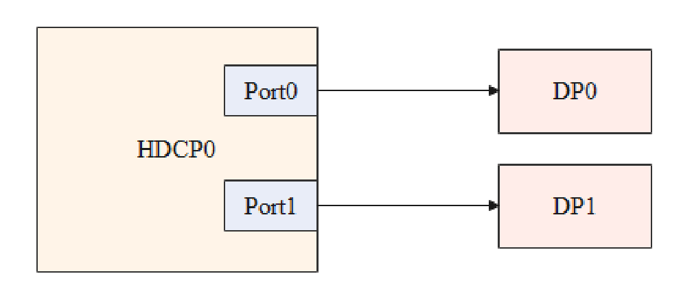
Enable these nodes for DP HDCP2.2:
&hdcp0 {
   status = "okay";

};
On RK3576, DP connects to HDCP1:
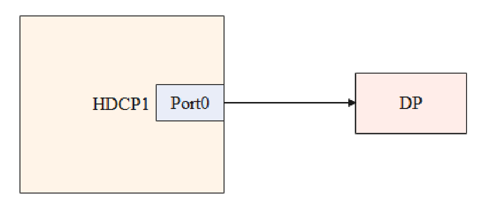
Enable these nodes for DP HDCP2.2:
&hdcp1 {
   status = "okay";

};
Besides driver configuration, HDCP2.2 requires enabling the userspace HDCP2.2 application and generating firmware for the HDCP controller. See Rockchip_RK3588_Developer_Guide_HDCP_CN.
2.9 dclk source configuration
DisplayPort commonly drives monitors that support multiple resolutions with different pixel clocks. To provide accurate dclk to the bound VOP Video Port at each pixel clock, the dclk source normally uses a PLL exclusively available to VOP, such as RK3588 V0PLL or RK3576 VPLL. If the default GPLL is used instead, resolutions whose dclk cannot be obtained by integer division may have inaccurate clocks and be filtered out.
2.9.1 RK3576 dclk source
On RK3576, /arch/arm64/boot/dts/rockchip/rk3576-evb.dtsi sets VP0’s dclk source to VPLL by default:
&vp0 {
      assigned-clocks = <&cru DCLK_VP0_SRC>;

      assigned-clock-parents = <&cru PLL_VPLL>;
};
If DP is bound to VP0, its dclk source is VPLL, permitting the required frequency division. If DP must use another VP, for example VP1, use this configuration:
&vp0 {
      /delete-property/ assigned-clocks;
      /delete-property/ assigned-clock-parents;

};

&vp1 {
      assigned-clocks = <&cru DCLK_VP1_SRC>;
      assigned-clock-parents = <&cru PLL_VPLL>;
};
This removes the dclk-source configuration from VP0 and adds it to VP1.
2.9.2 RK3588 dclk source
On RK3588, /arch/arm64/boot/dts/rockchip/rk3588s.dtsi sets VP2’s dclk source to V0PLL by default:
vp2: port@2 {
......
      assigned-clocks = <&cru DCLK_VOP2_SRC>;

      assigned-clock-parents = <&cru PLL_V0PLL>;
};
If DP is bound to VP2, its dclk source is V0PLL, permitting the required frequency division. If DP must use another VP, for example VP1, use:
&vp2 {
      /delete-property/ assigned-clocks;
      /delete-property/ assigned-clock-parents;

};

&vp1 {
      assigned-clocks = <&cru DCLK_VP1_SRC>;
      assigned-clock-parents = <&cru PLL_V0PLL>;
};
RK3588 has DP0 and DP1. If both are used simultaneously and bound to different VPs, for example DP0 to VP0 and DP1 to VP1, only one of VP0 and VP1 may use V0PLL as its dclk source. Otherwise the VP clock configurations interfere with one another and cause display errors.
3. Common debugging methods
3.1 Checking connector status
The /sys/class/drm directory lists the cards registered by the driver. In the following output, card0-DP-1 and card0-DP-2 are DP display devices.
rk3588_s:/ # ls /sys/class/drm/
card0    card0-DP-2 card0-HDMI-A-1 card0-Writeback-1 renderD128 version

card0-DP-1 card0-DSI-1 card0-HDMI-A-2 card1 renderD129
For example, card0-DP-1 contains:
rk3588_s:/ # ls /sys/class/drm/card0-DP-1/
device dpms edid enabled modes power status subsystem uevent
enabled: check whether the interface is enabled:
rk3588_s:/ # cat /sys/class/drm/card0-DP-1/enabled
disabled
status: check the connection state:
rk3588_s:/ # cat /sys/class/drm/card0-DP-1/status
disconnected
modes: list the resolutions supported by the device:
rk3588_s:/ # cat /sys/class/drm/card0-DP-1/modes
1440x900
1280x1024

1280x1024
1280x960
1152x864
1024x768
1024x768
832x624
800x600
800x600
640x480
640x480
720x400
edid: save the device EDID with:
rk3588_s:/ # cat /sys/class/drm/card0-DP-1/edid > /data/edid.bin
3.2 Forcing DP on or off
#强制禁⽤ DP
rk3588_s:/ # echo off > /sys/class/drm/card0-DP-1/status
#强制使能 DP

rk3588_s:/ # echo on > /sys/class/drm/card0-DP-1/status
#恢复热插拔检测
rk3588_s:/ # echo detect > /sys/class/drm/card0-DP-1/status
3.3 Reading and writing DPCD
DPCD is accessed through AUX_CH. The read/write node is implemented in:
/drivers/gpu/drm/drm_dp_aux_dev.c
Before using this function, verify that the required build option is enabled:
CONFIG_DRM_DP_AUX_CHARDEV=y
Reading DPCD:
#if 后⾯为 aux 节点,当注册两个 DP 接⼝时,会有 /dev/drm_dp_aux0 和 /dev/drm_dp_aux1
#skip 值为起始的 DPCD 寄存器地址
#count 值为要读取的 DPCD 寄存器的数量

dd if=/dev/drm_dp_aux0 bs=1 skip=$((0x00200)) count=2 status=none | od -tx1
#如下为读取地址为  0x00200 开始的 2 个 DPCD 寄存器的内容
rk3588_s:/ # dd if=/dev/drm_dp_aux1 bs=1 skip=$((0x00200)) count=2 status=none | od -tx1
0000000 01 00
0000002
Writing DPCD registers:
#echo 后为要写⼊的值, 如下为需要写⼊两个  16 进制的值,分别为 0x0a, 0x80
#of 后⾯为 aux 节点,当注册两个 DP 接⼝时,会有 /dev/drm_dp_aux0 和 /dev/drm_dp_aux1

#seek 后为起始的 DPCD 寄存器地址
#count 值为要写⼊的 DPCD 寄存器的数量
#如下指令为把  0x0a 和 0x80 两个值写⼊ 0x100 起始的两个 DPCD 寄存器处
echo -e -n "\x0a\x80" | dd of=/dev/drm_dp_aux0 bs=1 seek=$((0x100)) count=2 status=none
3.4 Type-C debugging
The PD controller detects Type-C HPD; the software flow is mainly handled by TCPM. Obtain the TCPM detection log as follows:
rk3588_s:/ # ls -l /sys/kernel/debug/usb/
total 0
-r--r--r-- 1 root root 0 1970-01-01 00:00 devices

drwxr-xr-x 18 root root 0 1970-01-01 00:00 fc000000.usb
drwxr-xr-x 2 root root 0 1970-01-01 00:00 fc400000.usb
-r--r--r-- 1 root root 0 1970-01-01 00:00 fusb302-2-0022
drwxr-xr-x 4 root root 0 1970-01-01 00:00 ohci
-r--r--r-- 1 root root 0 1970-01-01 00:00 tcpm-2-0022
drwxr-xr-x 2 root root 0 1970-01-01 00:00 usbmon
drwxr-xr-x 2 root root 0 2021-01-01 12:00 uvcvideo
drwxr-xr-x 3 root root 0 1970-01-01 00:00 xhci
In /sys/kernel/debug/usb/, fusb302-2-0022 is the PD-controller node and tcpm-2-0022 is the TCPM node. Read the TCPM log with:
cat /sys/kernel/debug/usb/tcpm-2-0022
In tcpm-2-0022, 2 denotes the i2c bus and 0022 the PD-controller i2c address.
Read the PD-controller log with:
cat /sys/kernel/debug/usb/fusb302-2-0022
In fusb302-2-0022, 2 denotes the i2c bus and 0022 the PD-controller address. This node corresponds to fusb302; other controllers have different node names.
Besides logs, further information is available under the Type-C node:
console:/ # ls /sys/class/typec
port0 port0-partner
port0 represents the SoC-side Type-C interface; port0-partner is the directory of the device connected through that interface.
Type-C connection orientation:
cat /sys/class/typec/port0/orientation
reverse
There may be multiple directories under port0-partner. The DP Alt Mode directory contains a displayport subdirectory and has svid equal to 0xff01.
ls -l /sys/class/typec/port0-partner/port0-partner.0/
total 0

-r--r--r-- 1 root root 4096 2022-04-14 14:50 active
-r--r--r-- 1 root root 4096 2022-04-14 14:50 description
drwxr-xr-x 2 root root 0 2022-04-14 14:50 displayport
lrwxrwxrwx 1 root root 0 2022-04-14 14:50 driver ->
../../../../../../../../../bus/typec/drivers/typec_displayport
-r--r--r-- 1 root root 4096 2022-04-14 14:50 mode
drwxr-xr-x 2 root root 0 2022-04-14 14:50 mode1
lrwxrwxrwx 1 root root 0 2022-04-14 14:50 port -> ../../port0.0
drwxr-xr-x 2 root root 0 2022-04-14 14:50 power
lrwxrwxrwx 1 root root 0 2022-04-14 14:50 subsystem ->

../../../../../../../../../bus/typec
-r--r--r-- 1 root root 4096 2022-04-14 14:50 svid
-rw-r--r-- 1 root root 4096 2022-04-14 14:50 uevent
-r--r--r-- 1 root root 4096 2022-04-14 14:50 vdo
cat /sys/class/typec/port0-partner/port0-partner.0/svid
ff01
Read the current pin assignment:
cat /sys/class/typec/port0-partner/port0-partner.0/displayport/pin_assignment
C [D]
#当前连接的设备⽀出  C assignment 和 D assignment, ⽬前配置的是 D assignment
These procedures apply to PD controllers using TCPM. For a PD controller not based on TCPM, confirm the information interfaces with its vendor.
3.5 Reading DP registers
RK3588 DP registers:
#dp0 控制器
cat /sys/kernel/debug/regmap/fde50000.dp/registers
#usbdp phy0

cmn_reg0000 - cmn_reg015D:
io -4 -r -l 1400 0xfed88000
trsv_reg0200 - trsv_reg03C3:
io -4 -r -l 1808 0xfed88800
trsv_reg0400 - trsv_reg0435:
io -4 -r -l 212 0xfed89000
trsv_reg0600 - trsv_reg07C3:
io -4 -r -l 1808 0xfed89800
trsv_reg0800 - trsv_reg0835:
io -4 -r -l 212 0xfed8A000
#dp1 控制器
cat /sys/kernel/debug/regmap/fde60000.dp/registers
#usbdp phy1

cmn_reg0000 - cmn_reg015D:
io -4 -r -l 1400 0xfed98000
trsv_reg0200 - trsv_reg03C3:
io -4 -r -l 1808 0xfed98800
trsv_reg0400 - trsv_reg0435:
io -4 -r -l 212 0xfed99000
trsv_reg0600 - trsv_reg07C3:
io -4 -r -l 1808 0xfed99800
trsv_reg0800 - trsv_reg0835:
io -4 -r -l 212 0xfed9A000
# vo0_grf
cat /sys/kernel/debug/regmap/dummy-syscon@fd5a6000/registers
RK3576 DP registers:
#dp 控制器
cat /sys/kernel/debug/regmap/27e40000.dp/registers
#usbdp phy

cmn_reg0000 - cmn_reg015D:
io -4 -r -l 1400 0x2b018000
trsv_reg0200 - trsv_reg03C3:
io -4 -r -l 1808 0x2b018800
trsv_reg0400 - trsv_reg0435:
io -4 -r -l 212 0x2b019000
trsv_reg0600 - trsv_reg07C3:
io -4 -r -l 1808 0x2b019800
trsv_reg0800 - trsv_reg0835:
io -4 -r -l 212 0x2b01a000
# vo1_grf
cat /sys/kernel/debug/regmap/dummy-syscon@0x0000000026036000/registers
PHY registers may be dumped only while a DP monitor is connected and displaying normally.
3.6 Checking VOP status
Query VOP status with:
cat /sys/kernel/debug/dri/0/summary
The resulting VOP status is shown below:
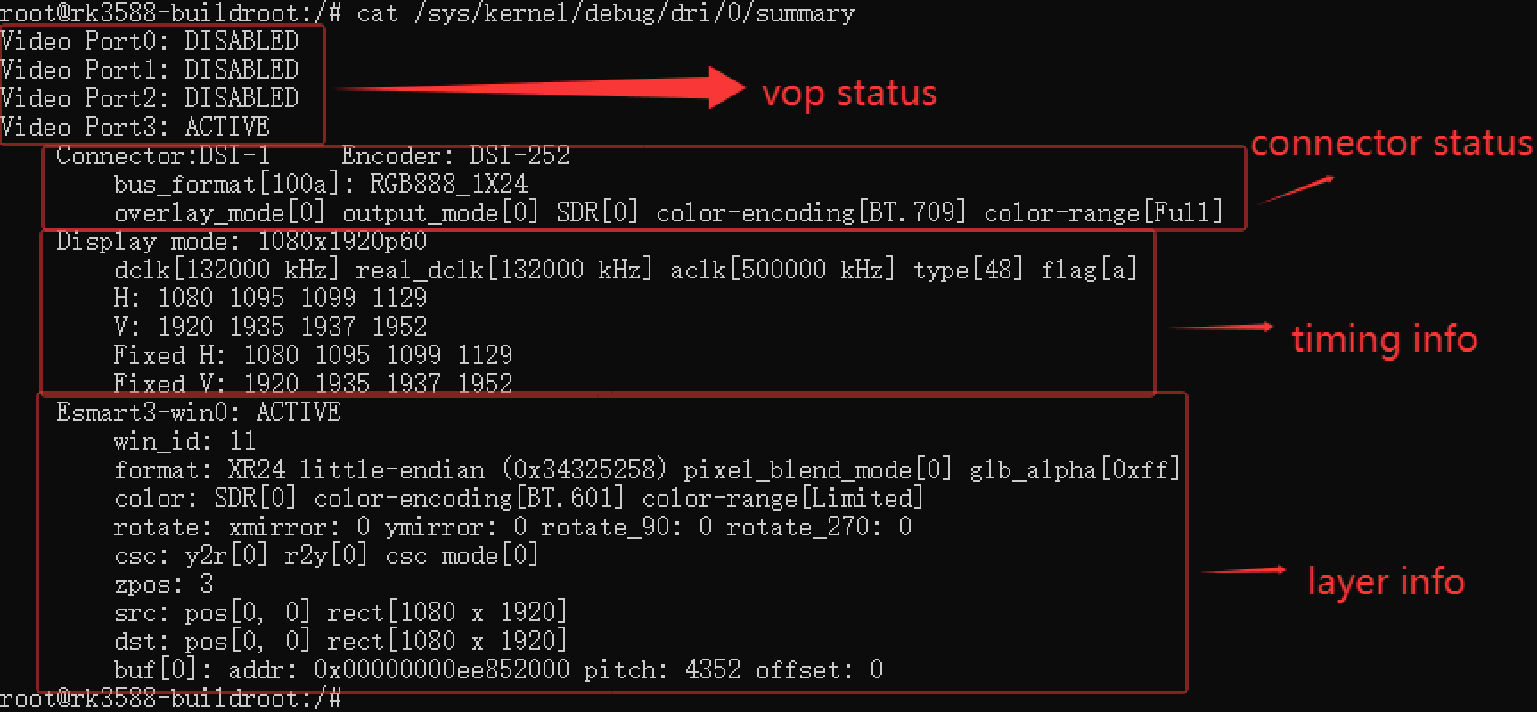
Video Portx: current Video Port state.
Connector: the output interface currently connected to the Video Port.
Display mode: the Video Port’s current output timing.
Clusterx-winx (Esmartx-winx): layer information.
In Kernel 6.1 and later, the output is:
root@linaro-alip:/# cat /sys/kernel/debug/dri/0/summary
Video Port0: ACTIVE

   Connector:DP-2 Encoder: DP-MST 0
      bus_format[100a]: RGB888_1X24
      overlay_mode[0] output_mode[f] SDR[0] color-encoding[BT.709] color-range[Limited]
   Display mode: 1280x720p60
      clk[74250] real_clk[74250] type[0] flag[5]
      H: 1280 1390 1430 1650
      V: 720 725 730 750
   Esmart0-win0: ACTIVE
      win_id: 0
      format: XR24 little-endian (0x34325258) pixel_blend_mode[0] glb_alpha[0xff]
      color: SDR[0] color-encoding[BT.601] color-range[Limited]
      rotate: xmirror: 0 ymirror: 0 rotate_90: 0 rotate_270: 0
      csc: y2r[0] r2y[0] csc mode[0]

      zpos: 0
      src: pos[0, 0] rect[1280 x 720]
      dst: pos[0, 0] rect[1280 x 720]
      buf[0]: addr: 0x0000000001017000 pitch: 5120 offset: 0
Video Port1: ACTIVE
   Connector:DP-5 Encoder: DP-MST 1
      bus_format[100a]: RGB888_1X24
      overlay_mode[0] output_mode[f] SDR[0] color-encoding[BT.709] color-range[Limited]
   Display mode: 1280x720p60
      clk[74250] real_clk[74250] type[0] flag[5]
      H: 1280 1390 1430 1650
      V: 720 725 730 750

   Esmart1-win0: ACTIVE
      win_id: 1
      format: XR24 little-endian (0x34325258) pixel_blend_mode[0] glb_alpha[0xff]
      color: SDR[0] color-encoding[BT.601] color-range[Limited]
      rotate: xmirror: 0 ymirror: 0 rotate_90: 0 rotate_270: 0
      csc: y2r[0] r2y[0] csc mode[0]
      zpos: 1
      src: pos[0, 0] rect[1280 x 720]
      dst: pos[0, 0] rect[1280 x 720]
      buf[0]: addr: 0x00000000001e1000 pitch: 5120 offset: 0
Video Port2: ACTIVE
   Connector:DP-6 Encoder: DP-MST 2
      bus_format[100a]: RGB888_1X24

      overlay_mode[0] output_mode[f] SDR[0] color-encoding[BT.709] color-range[Limited]
   Display mode: 1280x720p60
      clk[74250] real_clk[74250] type[0] flag[5]
      H: 1280 1390 1430 1650
      V: 720 725 730 750
   Esmart2-win0: ACTIVE
win_id: 2
format: XR24 little-endian (0x34325258) pixel_blend_mode[0] glb_alpha[0xff]
color: SDR[0] color-encoding[BT.601] color-range[Limited]

rotate: xmirror: 0 ymirror: 0 rotate_90: 0 rotate_270: 0
csc: y2r[0] r2y[0] csc mode[0]
zpos: 2
src: pos[0, 0] rect[1280 x 720]
dst: pos[0, 0] rect[1280 x 720]
buf[0]: addr: 0x00000000015e2000 pitch: 5120 offset: 0
The summary now also includes Encoder information.
RK3576 registers one SST Encoder and three MST Encoders. The three MST Encoders correspond to DP display streams as follows:
DP-MST 0 --> Stream-0
DP-MST 1 --> Stream-1

DP-MST 2 --> Stream-2
An MST Encoder indicates that DP is operating in MST mode. A DP Connector bound to a TMDS-xxx Encoder indicates SST mode. For example:
root@linaro-alip:/# cat /sys/kernel/debug/dri/0/summary
Video Port0: ACTIVE
   Connector:DP-1 Encoder: TMDS-184

      bus_format[1018]: RGB101010_1X30
      overlay_mode[0] output_mode[f] SDR[0] color-encoding[BT.709] color-range[Limited]
   Display mode: 1280x720p60
      clk[74250] real_clk[74250] type[0] flag[5]
      H: 1280 1390 1430 1650
      V: 720 725 730 750
   Esmart0-win0: ACTIVE
      win_id: 0
      format: XR24 little-endian (0x34325258) pixel_blend_mode[0] glb_alpha[0xff]
      color: SDR[0] color-encoding[BT.601] color-range[Limited]
      rotate: xmirror: 0 ymirror: 0 rotate_90: 0 rotate_270: 0
      csc: y2r[0] r2y[0] csc mode[0]

      zpos: 0
      src: pos[0, 0] rect[1280 x 720]
      dst: pos[0, 0] rect[1280 x 720]
      buf[0]: addr: 0x000000000090f000 pitch: 5120 offset: 0
Video Port1: DISABLED
Video Port2: DISABLED
3.7 Checking display clocks
Read the complete clock tree:
cat /sys/kernel/debug/clk/clk_summary
Read the DP AUX 16M clock:
cat /sys/kernel/debug/clk/clk_summary | grep -e "clk_aux16m_"
Read VOP dclk:
cat /sys/kernel/debug/clk/clk_summary | grep -e "dclk"
3.8 Adjusting DRM log levels
DRM defines the following logging categories. Enable the needed categories dynamically:
enum drm_debug_category {
      /**
      * @DRM_UT_CORE: Used in the generic drm code: drm_ioctl.c, drm_mm.c,

      * drm_memory.c, ...
      */
      DRM_UT_CORE      = 0x01,
      /**
      * @DRM_UT_DRIVER: Used in the vendor specific part of the driver: i915,
      * radeon, ... macro.
      */
      DRM_UT_DRIVER    = 0x02,
      /**
      * @DRM_UT_KMS: Used in the modesetting code.
      */
      DRM_UT_KMS       = 0x04,
      /**

      * @DRM_UT_PRIME: Used in the prime code.
      */
      DRM_UT_PRIME     = 0x08,
      /**
      * @DRM_UT_ATOMIC: Used in the atomic code.
      */
      DRM_UT_ATOMIC    = 0x10,
      /**
      * @DRM_UT_VBL: Used for verbose debug message in the vblank code.
      */
      DRM_UT_VBL       = 0x20,
      /**

      * @DRM_UT_STATE: Used for verbose atomic state debugging.
      */
      DRM_UT_STATE     = 0x40,
      /**
      * @DRM_UT_LEASE: Used in the lease code.
      */
      DRM_UT_LEASE     = 0x80,
      /**
      * @DRM_UT_DP: Used in the DP code.
      */
      DRM_UT_DP        = 0x100,
      /**
      * @DRM_UT_DRMRES: Used in the drm managed resources code.

      */
      DRM_UT_DRMRES    = 0x200,
};
For DP debugging, particularly commit failures, ATOMIC logging is commonly used:
echo 0x10 > /sys/module/drm/parameters/debug
For DPCD read/write logging, run:
echo 0x100 > /sys/module/drm/parameters/debug
3.9 DP driver debug logging
The DP driver uses drm_dbg_dp for debug messages. Enable dynamic DP logging with:
echo 0x100 > /sys/module/drm/parameters/debug
3.10 Reading DP Status
Read DP Status with:
cat /sys/kernel/debug/dri/0/dw-dp0/dp_status
dw-dp0 identifies the physical DP interface. RK3576 has one physical DP interface, so use dw-dp0. RK3588 has two, represented by dw-dp0 and dw-dp1.
On RK3576 with normal DP output, the command produces:
HPD:
      force hpd: no
      gpio hpd: no

      usbdp hpd: no
      hpd status: plug
AUX: normal
LINK:
      link lanes: 4
      link rate: 5400 MHz
      ssc: enable
      cr done:yes
      eq done:yes
DP mode: SST
DP Stream0: active
      Video Info:
            video enable: yes
            video format: RGB_10BIT

            scan mode: process
            hactive: 3840 hfp: 176   hsync: 88   hblank: 560  hsync
pol: 1
            vactive: 2160 vfp: 8     vsync: 10   vblank: 90   vsync
pol: 1
      MSA Info:
            misc0 : 0x40
            misc1 : 0x00
            Pixel Encoding/Colorimetry format: RGB
            Color Depth: 10 bpc
      SDP Bank00 Info:
            vertical ctrl: no

            horizontal ctrl: no
      SDP Bank01 Info:
            vertical ctrl: no
            horizontal ctrl: no
      SDP Bank02 Info:
            vertical ctrl: no
            horizontal ctrl: no
      SDP Bank03 Info:
            vertical ctrl: no
            horizontal ctrl: no
      SDP Bank04 Info:
            vertical ctrl: no
            horizontal ctrl: no

      SDP Bank05 Info:
            vertical ctrl: no
            horizontal ctrl: no
      SDP Bank06 Info:
            vertical ctrl: no
            horizontal ctrl: no
      SDP Bank07 Info:
            vertical ctrl: no
            horizontal ctrl: no
      SDP Bank08 Info:
            vertical ctrl: no
            horizontal ctrl: no

      SDP Bank09 Info:
            vertical ctrl: no
            horizontal ctrl: no
      SDP Bank10 Info:
            vertical ctrl: no
            horizontal ctrl: no
      SDP Bank11 Info:
            vertical ctrl: no
            horizontal ctrl: no
      SDP Bank12 Info:
            vertical ctrl: no
            horizontal ctrl: no
      SDP Bank13 Info:
     vertical ctrl: no
     horizontal ctrl: no
SDP Bank14 Info:

     vertical ctrl: no
     horizontal ctrl: no
SDP Bank15 Info:
     vertical ctrl: no
     horizontal ctrl: no
3.10.1 HPD Status
HPD information includes the HPD type and state:
force hpd: yes means force-hpd is configured in DTS.
gpio hpd: yes means an ordinary GPIO is configured as the HPD pin in DTS.
usbdp hpd: yes means the Type-C HPD state is delivered to the DP driver through TCPM.
hpd status: plug means HPD is asserted; unplug means HPD is not asserted.
3.10.2 AUX Status
AUX: normal indicates normal AUX access; wrong indicates an AUX access error.
3.10.3 LINK Status
The LINK section describes the link after training:
link lanes: the selected number of lanes after training, either 1, 2 or 4.
link rate: the rate selected after training: 1620MHz, 2700MHz, 5400MHz or 8100MHz.
ssc: enable means SSC is enabled; disable means it is disabled.
cr done: yes means the clock-recovery phase of link training passed.
eq done: yes means the channel-equalization phase of link training passed.
3.10.4 DP Mode Status
DP mode: SST or MST indicates the current DP transport mode.
3.10.5 DP Stream Status
An SST-only interface has information for one DP stream; an MST-capable interface has information for multiple streams.
DP Streamx: active means this DP Stream is enabled.
Video Info describes the current DP-controller output configuration:
video enable: yes outputs the image supplied by VOP; no outputs the continuously generated DP-controller pattern.
video format describes color depth and format. For example, RGB_10BIT means RGB data with 10-bit depth.
scan mode: the source spells the progressive value preocess; interlace indicates interlaced scanning.
hactive, hfp, hsync, hblank, hsync pol, vatctive, vfp, vsync, vblank and vsync pol describe the current output scan timing. The source spelling vatctive is retained.
MSA Info communicates the output DP stream configuration to DPRX:
misc0: raw, undecoded misc0 data.
misc1: the source describes this as raw, undecoded misc0 data; the inconsistent field name is retained for review.
Pixel Encoding/Colorimetry format describes the colorimetry and range. RGB means RGB full range; CEA RGB means RGB limited range.
YUV options include YCBCR 422 BT601, YCBCR 422 BT709, YCBCR 444 BT601 and YCBCR 444 BT709; these use limited range. The source says YUV420, BT2020 or YUV limited range requires VSC SDP, in which case this field shows use VSC SDP.
Color Depth describes the transmitted color depth; the source lists 6 bpc, 8 bpc and 12 bpc. If color information is sent with VSC SDP, it shows use VSC SDP.
SDP Bankx Info indicates whether SDP Bankx is used to transmit SDP packets:
vertical ctrl: yes means the SDP in this bank is transmitted during vblank; no means it is not transmitted during vblank.
horizontal ctrl: yes means transmission during hblank; no means no transmission during hblank.
header: SDP packet header; decode it according to the DP specification.
payload: SDP payload; decode it according to the DP specification.
The following is part of the DP Stream information for 4K60Hz transmitted in YUV420:
DP mode: SST
DP Stream0: active
      Video Info:

           video enable: yes
           video format: YCBCR420_8BIT
           scan mode: process
           hactive: 3840 hfp: 178   hsync: 88   hblank: 560   hsync
pol: 1
           vactive: 2160 vfp: 8     vsync: 10   vblank: 90    vsync
pol: 1
      MSA Info:
           misc0 : 0x20
           misc1 : 0x40

           Pixel Encoding/Colorimetry format: use VSC SDP
           Color Depth: use VSC SDP
      SDP Bank00 Info:
           vertical ctrl: no
           horizontal ctrl: no
      SDP Bank01 Info:
           vertical ctrl: yes
           horizontal ctrl: no
           header: 00 07 05 13
           payload: 00 00 00 00 00 00 00 00 00 00 00 00 00 00 00 00 31 81 00 00 00 00
00 00 00 00 00 00 00 00 00 00
For YUV420, both Pixel Encoding/Colorimetry format and Color Depth show use VSC SDP. SDP Bank01 Info shows that SDP Bank01 transmits VSC SDP during vblank.
3.11 Reading DP MST information
Read DP MST information with:
cat /sys/kernel/debug/dri/0/dw-dp0/dp_mst_info
dw-dp0 denotes the physical DP interface. RK3576 has only one and uses dw-dp0. RK3588 does not support DP MST and does not use this node.
With three RK3576 MST outputs displaying normally, the command returns:
root@linaro-alip:/# cat /sys/kernel/debug/dri/0/dw-dp0/dp_mst_info
      mstb - [000000003a17fc25]: num_ports: 4
      port 3 - [00000000099bbb63] (output - SST SINK): ddps: 1, ldps: 0, sdp: 1/1, fec:

false, conn: 00000000c74ff83b
      port 2 - [00000000505d66cf] (output - MST BRANCHING): ddps: 1, ldps: 0, sdp: 0/0,
fec: true, conn: 00000000b57a2623
           mstb - [0000000090afd0f3]: num_ports: 3
           port 1 - [00000000072aa867] (output - NONE): ddps: 0, ldps: 0, sdp: 0/0,
fec: false, conn: 000000005ba2b268
           port 8 - [0000000046d78f33] (output - SST SINK): ddps: 1, ldps: 0, sdp: 1/2,
fec: true, conn: 000000002668a7af
           port 0 - [00000000a70f650f] (input - NONE): ddps: 1, ldps: 0, sdp: 0/0, fec:
false, conn: 0000000000000000
      port 1 - [000000003fd2f64a] (output - SST SINK): ddps: 1, ldps: 0, sdp: 1/1, fec:
false, conn: 000000005ff7f122

      port 0 - [00000000c8a5769d] (input - NONE): ddps: 1, ldps: 0, sdp: 0/0, fec: false,
conn: 0000000000000000

*** Atomic state info ***
payload_mask: 7, max_payloads: 3, start_slot: 1, pbn_div: 60
| idx | port | vcpi | slots | pbn | dsc | sink name |
   1     1    1 06 - 10 266 N          U27U2D
   2     8    2 11 - 15 266 N      DELL U2723QE

   3     3    3 01 - 05 266 N         U28E590

*** DPCD Info ***
dpcd: 14 1e c4 81 01 11 01 83 2a 3f 04 00 00 00 84
faux/mst: 00 01
mst ctrl: 07
branch oui: 90cc24 devid: SYNAS revision: hw: 1.0 sw: 5.5
payload table: 03 03 03 03 03 03 01 01 01 01 01 02 02 02 02 02 00 00 00 00 00 00 00 00 00 00
00 00 00 00 00 00 00 00 00 00 00 00 00 00 00 00 00 00 00 00 00 00 00 00 00 00 00 00 00 00 00
00 00 00 00 00 00 00

*** Connector path info ***

connector name | connector path
DP-2        mst:185-1
DP-3        mst:185-2
DP-6        mst:185-3
DP-5        mst:185-2-8
DP-7        mst:185-2-1
3.11.1 MST Port Info
The first part describes the device connection topology.
      mstb - [000000003a17fc25]: num_ports: 4
      port 3 - [00000000099bbb63] (output - SST SINK): ddps: 1, ldps: 0, sdp: 1/1, fec:
false, conn: 00000000c74ff83b

      port 2 - [00000000505d66cf] (output - MST BRANCHING): ddps: 1, ldps: 0, sdp: 0/0,
fec: true, conn: 00000000b57a2623
           mstb - [0000000090afd0f3]: num_ports: 3
           port 1 - [00000000072aa867] (output - NONE): ddps: 0, ldps: 0, sdp: 0/0,
fec: false, conn: 000000005ba2b268
           port 8 - [0000000046d78f33] (output - SST SINK): ddps: 1, ldps: 0, sdp: 1/2,
fec: true, conn: 000000002668a7af
           port 0 - [00000000a70f650f] (input - NONE): ddps: 1, ldps: 0, sdp: 0/0, fec:
false, conn: 0000000000000000
      port 1 - [000000003fd2f64a] (output - SST SINK): ddps: 1, ldps: 0, sdp: 1/1, fec:
false, conn: 000000005ff7f122
      port 0 - [00000000c8a5769d] (input - NONE): ddps: 1, ldps: 0, sdp: 0/0, fec: false,
conn: 0000000000000000
As described in the DP-output section (the source cites section 1.1.3), RK3576 MST requires an MST HUB or MST monitor. Each input and output port has an independent number. The following HUB has one input and three outputs; the source mistakenly calls both groups outputs.
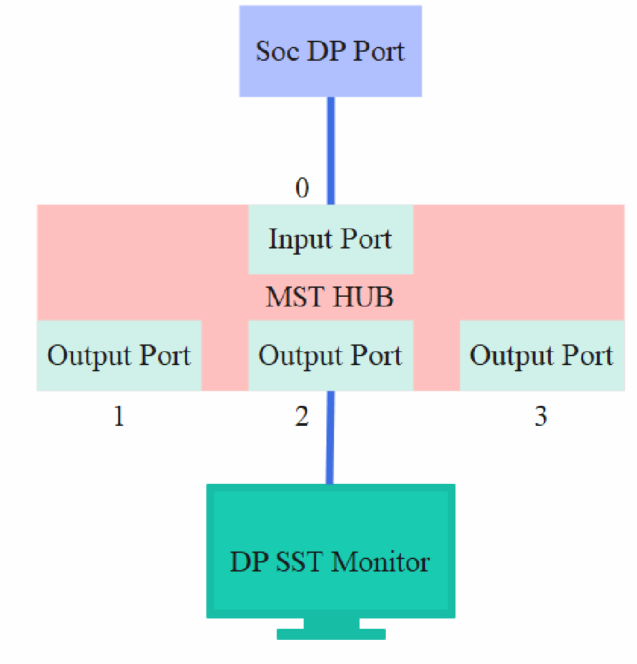
These are physical ports that connect to external devices. DP assigns physical ports numbers 0–7, with input-port numbers lower than output-port numbers. An MST HUB normally starts numbering at 0. This HUB has four ports: Port0 is input, Port1/2/3 are outputs. Port2 connects to an SST monitor, producing this topology:
      mstb - [00000000c8269fca]: num_ports: 4
      port 3 - [0000000007690f7c] (output - NONE): ddps: 0, ldps: 0, sdp: 0/0, fec: false,
conn: 00000000d0584c6f

      port 2 - [00000000812cc57a] (output - SST SINK): ddps: 1, ldps: 0, sdp: 1/1, fec:
false, conn: 000000001ef4a070
      port 1 - [00000000efb170aa] (output - NONE): ddps: 0, ldps: 0, sdp: 0/0, fec: false,
conn: 000000001455081f
      port 0 - [000000005aa73543] (input - NONE): ddps: 1, ldps: 0, sdp: 0/0, fec: false,
conn: 0000000000000000
An MST monitor normally has one DP input and one DP output as shown below; the source repeats ‘input’ for both.
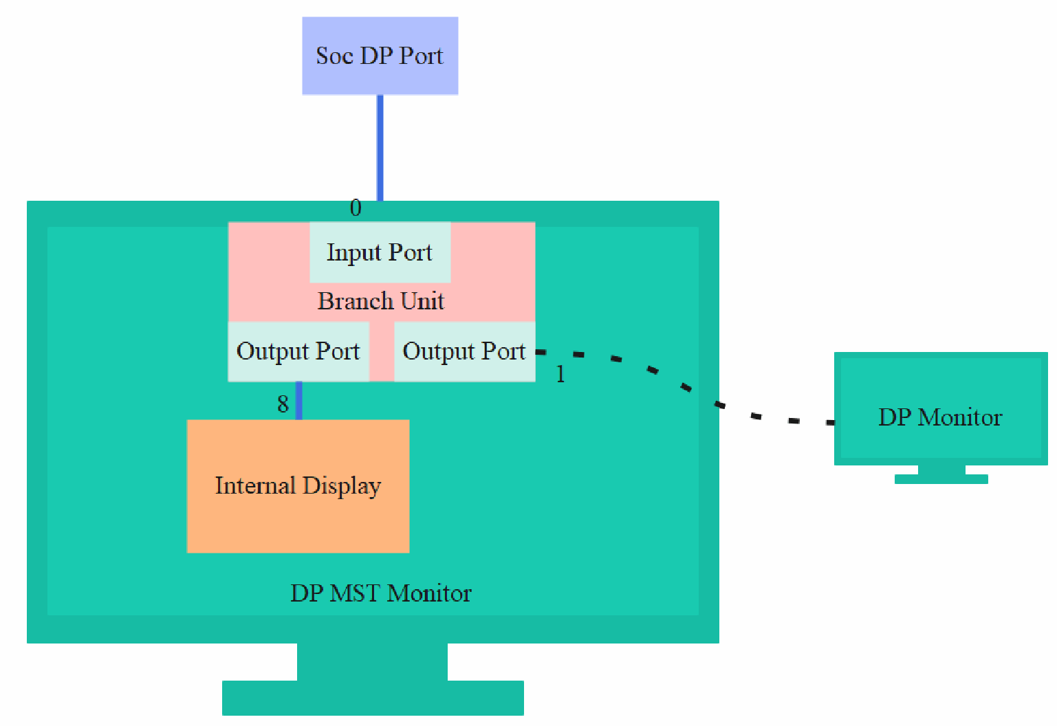
Here Port0 is the input, Port1 the output, and Port8 an internal monitor output. Such internal ports are logical ports, numbered 8–15. With no additional monitor daisy-chained, the topology is:
      mstb - [0000000019f71241]: num_ports: 3
      port 1 - [0000000095fb1fc0] (output - NONE): ddps: 0, ldps: 0, sdp: 0/0, fec: false,
conn: 000000004d03ffa2

      port 8 - [00000000a66da753] (output - SST SINK): ddps: 1, ldps: 0, sdp: 1/2, fec:
true, conn: 000000009a417589
      port 0 - [000000009a0122a8] (input - NONE): ddps: 1, ldps: 0, sdp: 0/0, fec: false,
conn: 0000000000000000
3.11.2 Atomic state info
In MST mode, the basic DP packet is the Multi-Stream Transport Packet (MTP). It contains 64 link symbols, also called time slots, numbered 0–63. Time slot 0 is MTPH; the remaining slots carry display-stream data. The MTP format is shown below.
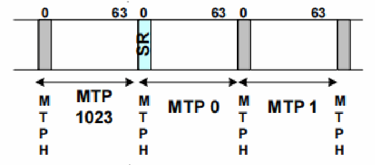
In payload info below, port is the MST-device port number, vcpi the display-stream number, slots the time slots occupied by that stream, pbn its bandwidth allocation, and sink name the monitor name.
| idx | port | vcpi | slots | pbn | dsc | sink name |
   1     1    1 06 - 10 266 N          U27U2D
   2     8    2 11 - 15 266 N      DELL U2723QE

   3     3    3 01 - 05 266 N         U28E590
3.11.3 DPCD Info
This section contains the DPCD data. Pay particular attention to the payload table, which records the detailed time-slot allocation.
*** DPCD Info ***
dpcd: 14 1e c4 81 01 11 01 83 2a 3f 04 00 00 00 84
faux/mst: 00 01

mst ctrl: 07
branch oui: 90cc24 devid: SYNAS revision: hw: 1.0 sw: 5.5
payload table: 03 03 03 03 03 03 01 01 01 01 01 02 02 02 02 02 00 00 00 00 00 00 00 00 00 00
00 00 00 00 00 00 00 00 00 00 00 00 00 00 00 00 00 00 00 00 00 00 00 00 00 00 00 00 00 00 00
00 00 00 00 00 00 00
3.11.4 Connector Path Info
connector name is the dynamically registered DP connector; connector path is its corresponding path. The source misspells these as connecor and connecotr.
*** Connector path info ***
connector name | connector path

DP-2        mst:185-1
DP-3        mst:185-2
DP-6        mst:185-3
DP-5        mst:185-2-8
DP-7        mst:185-2-1
4. FAQ
4.1 No display or abnormal display after connecting DP
First check for the following log:
[  14.857002] rockchip-vop2 fdd90000.vop: [drm:vop2_crtc_atomic_enable] Update mode to
1920x1080p60, type: 10(if:200) for vp2 dclk: 148500000
[  14.857149] rockchip-vop2 fdd90000.vop: [drm:vop2_crtc_atomic_enable] dclk_out2 div: 2

dclk_core2 div: 2
[  14.857868] rockchip-vop2 fdd90000.vop: [drm:vop2_crtc_atomic_enable] set dclk_vop2 to
148500000, get 148500000
[  14.872406] dw-dp fde50000.dp: full-training link: 2 lanes at 5400 MHz
[  14.893269] dw-dp fde50000.dp: clock recovery succeeded
[  14.899797] dw-dp fde50000.dp: channel equalization succeeded
4.1.1 DP link training succeeded
This log means the DP connection was detected, link training succeeded and image output started. A blank or abnormal display can have the following causes:
(1) Inaccurate dclk division
The following log requests 25.175MHz dclk but receives 20MHz. For this clock-allocation problem, collect the complete log and clock-tree log for further analysis.
[ 268.733803] rockchip-vop2 fdd90000.vop: [drm:vop2_crtc_atomic_disable] Crtc atomic disable
vp2
[ 268.759178] rockchip-vop2 fdd90000.vop: [drm:vop2_crtc_atomic_enable] Update mode to

640x480p60, type: 10(if:200) for vp2 dclk: 25175000
[ 268.759447] rockchip-vop2 fdd90000.vop: [drm:vop2_crtc_atomic_enable] dclk_out2 div: 2
dclk_core2 div: 2
[ 268.759665] rockchip_rk3588_pll_set_rate: Invalid rate : 25175000 for pll clk pll_v0pll
[ 268.759715] rockchip-vop2 fdd90000.vop: [drm:vop2_crtc_atomic_enable] set dclk_vop2 to
25175000, get 20000000
[ 268.775591] dw-dp fde50000.dp: full-training link: 4 lanes at 2700 MHz
[ 268.790059] dw-dp fde50000.dp: clock recovery succeeded
[ 268.795376] dw-dp fde50000.dp: channel equalization succeeded
(2) No layer allocated
If userspace has not allocated a layer, run cat /sys/kernel/debug/dri/0/summary. If the output contains no layer information as shown below, investigate userspace further.
rk3588_s:/ # cat /sys/kernel/debug/dri/0/summary
Video Port0: DISABLED

Video Port1: DISABLED
Video Port2: DISABLED
Video Port3: ACTIVE
   Connector: DSI-1
      bus_format[100a]: RGB888_1X24
      overlay_mode[0] output_mode[0] color_space[0], eotf:0
   Display mode: 1080x1920p60
      clk[132000] real_clk[132000] type[48] flag[a]
      H: 1080 1095 1099 1129
      V: 1920 1935 1937 1952
4.1.2 DP connected
If the log at the start of this section is absent, first read the DP connection status:
cat /sys/class/drm/card0-DP-1/status
If DP is connected, inspect the log for errors and investigate them first. If no error is logged, enable DRM ATOMIC logging and reproduce the issue. Check whether drm atomic commit returns prematurely because an atomic-check stage failed.
4.1.3 DP disconnected
For a standard DP port, verify HPD configuration and hardware connections. For Type-C, use the connection-failure analysis below.
4.2 Type-C connection failure
Here Type-C connection failure means an error during the CC or PD stage. First obtain DP connection status:
cat /sys/class/drm/card0-DP-1/status
When the connection fails, the state is disconnected.
Read the TCPM log through its debug node:
cat /sys/kernel/debug/usb/tcpm-2-0022
A normal connection produces the following log:
[  25.026952] AMS DISCOVER_IDENTITY start
[  25.026967] PD TX, header: 0x176f

[  25.035314] PD TX complete, status: 0
[  25.042866] PD RX, header: 0x524f [1]
[  25.042880] Rx VDM cmd 0xff00a041 type 1 cmd 1 len 5
[  25.042894] AMS DISCOVER_IDENTITY finished
[  25.042898] cc:=4
[  25.052343] Identity: 04e8:a020.0212
[  25.052364] AMS DISCOVER_SVIDS start
[  25.052372] PD TX, header: 0x196f
[  25.061314] PD TX complete, status: 0
[  25.067667] PD RX, header: 0x344f [1]
[  25.067680] Rx VDM cmd 0xff00a042 type 1 cmd 2 len 3
[  25.067695] AMS DISCOVER_SVIDS finished
[  25.067705] cc:=4

[  25.077097] SVID 1: 0xff01
[  25.077114] SVID 2: 0x4e8
[  25.077129] AMS DISCOVER_MODES start
[  25.077135] PD TX, header: 0x1b6f
[  25.086092] PD TX complete, status: 0
[  25.092224] PD RX, header: 0x264f [1]
[  25.092237] Rx VDM cmd 0xff01a043 type 1 cmd 3 len 2

[  25.092252] AMS DISCOVER_MODES finished
[  25.092256] cc:=4
[  25.101432] Alternate mode 0: SVID 0xff01, VDO 1: 0x00000c05
[  25.101517] AMS DISCOVER_MODES start
[  25.101526] PD TX, header: 0x1d6f
[  25.109717] PD TX complete, status: 0
[  25.114919] PD RX, header: 0x284f [1]
[  25.114937] Rx VDM cmd 0x4e8a043 type 1 cmd 3 len 2
[  25.114951] AMS DISCOVER_MODES finished
[  25.114956] cc:=4
[  25.124604] Alternate mode 1: SVID 0x04e8, VDO 1: 0x00000001
[  25.125676] AMS DFP_TO_UFP_ENTER_MODE start

[  25.125686] PD TX, header: 0x1f6f
[  25.134560] PD TX complete, status: 0
[  25.137903] PD RX, header: 0x1a4f [1]
[  25.137917] Rx VDM cmd 0xff01a144 type 1 cmd 4 len 1
[  25.137930] AMS DFP_TO_UFP_ENTER_MODE finished
[  25.137936] cc:=4
[  25.145828] AMS STRUCTURED_VDMS start
[  25.145836] PD TX, header: 0x216f
[  25.154942] PD TX complete, status: 0
[  25.161111] PD RX, header: 0x2c4f [1]
[  25.161125] Rx VDM cmd 0xff01a150 type 1 cmd 16 len 2 //STATUS UPDATE
[  25.161138] AMS STRUCTURED_VDMS finished
[  25.161142] cc:=4

[  25.171888] AMS STRUCTURED_VDMS start
[  25.171911] PD TX, header: 0x236f
[  25.182016] PD TX complete, status: 0
[  25.185550] PD RX, header: 0x1e4f [1]
[  25.185563] Rx VDM cmd 0xff01a151 type 1 cmd 17 len 1 //CONFIGURATION
[  25.185577] AMS STRUCTURED_VDMS finished
[  25.185581] cc:=4
[  26.392673] PD RX, header: 0x204f [1]
[  26.392687] Rx VDM cmd 0xff018106 type 0 cmd 6 len 2 //ATTENTION
A complete normal sequence exchanges DISCOVER_IDENTITY, DISCOVER_MODES, DFP_TO_UFP_ENTER_MODE, STATUS UPDATE, CONFIGURATION and ATTENTION commands. If these exchanges are absent, PD negotiation is abnormal.
If that sequence fails, the source suggests testing with a higher PD-controller I2C speed. If the problem remains, supply complete TCPM and PD-controller logs for further analysis.
4.3 AUX_CH failure
AUX_CH failures cause DPCD read/write and EDID-read failures. The log may contain:
[ 1368.952182] dw-dp fde50000.dp: failed to probe DP link: -110
If uncertain, enable this DRM debug-log switch:
echo 0x100 > /sys/module/drm/parameters/debug
Read the DPCD access log using dmesg. Normal accesses have ret equal to 0 (the source misspells DPCD as DPCP):
[ 6329.554538] rockchip-drm display-subsystem: [drm:drm_dp_dpcd_probe] fde50000.dp: 0x00000
AUX -> (ret= 1) 12

[ 6329.554939] rockchip-drm display-subsystem: [drm:drm_dp_dpcd_read] fde50000.dp: 0x00000
AUX -> (ret= 15) 12 14 c2 81 01 01 01 81 02 02 06 00 00 00 81
[ 6329.555383] rockchip-drm display-subsystem: [drm:drm_dp_dpcd_probe] fde50000.dp: 0x00000
AUX -> (ret= 1) 12
For an AUX_CH error, ret contains the error-type value:
[  31.116976] rockchip-drm display-subsystem: [drm:drm_dp_dpcd_probe] fde50000.dp: 0x00000
AUX -> (ret=-110)
Possible causes include:
4.3.1 Incorrect aux16m clock
The aux16m parent is GPLL, normally configured to 1188MHz. The default aux16m rate is shown below:
root@RK3588:/# cat /sys/kernel/debug/clk/clk_summary | grep "aux16m"
       clk_aux16m_1        1      2     0   15840000     0    0
50000

       clk_aux16m_0        1      2     0   15840000     0    0
50000
If GPLL is not 1188MHz and aux16m is also non-default, check for changes from the SDK in /drivers/clk/rockchip/ or a reconfigured VOP DCLK parent.
4.3.2 Abnormal PHY power-on/off flow
This commonly occurs when USB and Type-C share a PHY. If Type-C works in one orientation but fails in the other, the USB PHY may not have exited on unplug, preventing reinitialization on the next insertion. Add logs to verify PHY power-on/off during USB insertion/removal and PHY reinitialization after reversing the connector. The following patch illustrates logging.
diff --git a/drivers/phy/rockchip/phy-rockchip-usbdp.c b/drivers/phy/rockchip/phy-rockchip-usbdp.c

index c6fc4a2aa558..6b35e12f40aa 100644
--- a/drivers/phy/rockchip/phy-rockchip-usbdp.c
+++ b/drivers/phy/rockchip/phy-rockchip-usbdp.c
@@ -823,6 +823,7 @@ static int udphy_power_on(struct rockchip_udphy *udphy, u8 mode)
 {
      int ret;


+     dev_info(udphy->dev, "%s status:%x, mode:%x\n", __func__, udphy->status, mode);
      if (!(udphy->mode & mode)) {
            dev_info(udphy->dev, "mode 0x%02x is not support\n", mode);
            return 0;
@@ -859,6 +860,7 @@ static int udphy_power_off(struct rockchip_udphy *udphy, u8 mode)
 {
      int ret;

+     dev_info(udphy->dev, "%s status:%x, mode:%x\n", __func__, udphy->status, mode);
      if (!(udphy->mode & mode)) {
            dev_info(udphy->dev, "mode 0x%02x is not support\n", mode);
            return 0;

@@ -883,6 +885,7 @@ static int rockchip_dp_phy_power_on(struct phy *phy)
      struct rockchip_udphy *udphy = phy_get_drvdata(phy);
      int ret, dp_lanes;

+     dev_info(udphy->dev, "%s\n", __func__);
      mutex_lock(&udphy->mutex);

      dp_lanes = udphy_dplane_get(udphy);
@@ -914,6 +917,7 @@ static int rockchip_dp_phy_power_off(struct phy *phy)
      struct rockchip_udphy *udphy = phy_get_drvdata(phy);
      int ret;

+     dev_info(udphy->dev, "%s\n", __func__);

      mutex_lock(&udphy->mutex);
      ret = udphy_dplane_enable(udphy, 0);
      if (ret)
@@ -1028,6 +1032,7 @@ static int rockchip_u3phy_init(struct phy *phy)
      struct rockchip_udphy *udphy = phy_get_drvdata(phy);
      int ret = 0;

+     dev_info(udphy->dev, "%s\n", __func__);
      mutex_lock(&udphy->mutex);
      /* DP only or high-speed, disable U3 port */
      if (!(udphy->mode & UDPHY_MODE_USB) || udphy->hs) {
@@ -1047,6 +1052,7 @@ static int rockchip_u3phy_exit(struct phy *phy)

      struct rockchip_udphy *udphy = phy_get_drvdata(phy);
      int ret = 0;

+     dev_info(udphy->dev, "%s\n", __func__);
      mutex_lock(&udphy->mutex);
      /* DP only or high-speed */
      if (!(udphy->mode & UDPHY_MODE_USB) || udphy->hs)
@@ -1363,6 +1369,7 @@ static int rk3588_udphy_init(struct rockchip_udphy *udphy)
      const struct rockchip_udphy_cfg *cfg = udphy->cfgs;
      int ret;

+     dev_info(udphy->dev, "%s\n", __func__);
      /* enable rx lfps for usb */
if (udphy->mode & UDPHY_MODE_USB)
     grfreg_write(udphy->udphygrf, &cfg->grfcfg.rx_lfps, true);
4.3.3 DP dual-mode adapter failure
DP dual mode requires a DP port to support both DP output and HDMI TMDS transmission, with AUX supporting both DP AUX and DDC (I2C).
RK3588 DP does not support DP dual mode. Connecting a dual-mode cable can cause AUX_CH errors, typically with standard-DP-to-HDMI cables or converters. If AUX_CH fails with such a cable and the cable supports an HDMI version below 2.0, it may be a dual-mode adapter. The source recommends trying an adapter supporting HDMI 2.0 or later; verify the actual active-converter design rather than assuming the version label alone guarantees compatibility.
4.3.4 Signal interference
This often occurs with direct Type-C connections when USB DP/DM signals interfere with DP AUX. As a hardware diagnostic, disconnect USB DP/DM and see whether the problem recurs. Solutions described by the source are a better-quality Type-C cable with proper inter-signal shielding, or not using USB DP/DM for data.
4.3.5 Hardware failure
First verify the hardware path, AUX differential-signal transmission and solder joints. Then check that the AUX_CH peripheral circuit follows the DP specification. If a converter chip is used, verify its surrounding circuitry first.
4.4 Configuring 4K 120Hz output
RK3588 VOP ACLK defaults to 500M. High-pixel-clock output such as 4K 120Hz can exceed its performance and produce the following display error:
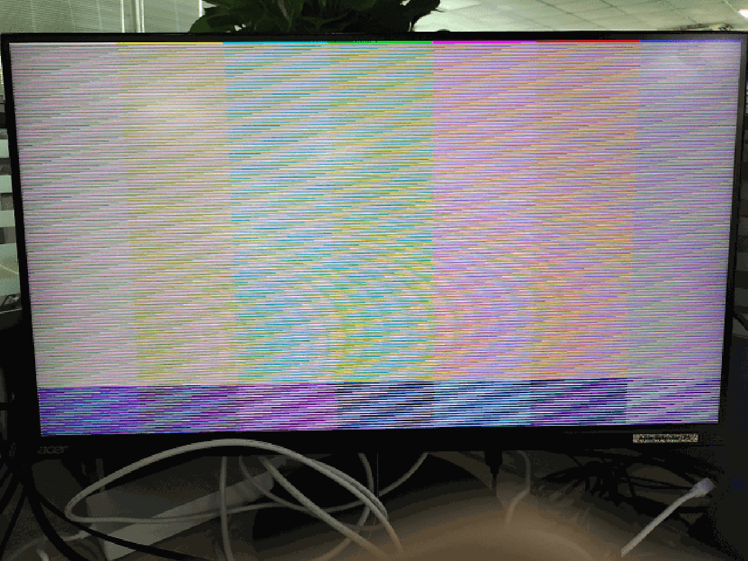
For this problem, the source raises VOP ACLK to 800M:
&vop {
   assigned-clocks = <&cru ACLK_VOP>;

   assigned-clock-rates = <800000000>;
};
Read VOP ACLK with:
cat /sys/kernel/debug/clk/clk_summary | grep "aclk_vop"
4.5 DP bandwidth calculation
4.5.1 SST bandwidth
Calculate the required bandwidth per DP lane using:
bandwidth_per_lane = pixel_clk * bit_per_pixel * 1.25 / lane_count
bit_per_pixel is the number of bits per pixel, 1.25 is the PHY encoding factor, and lane_count is the number of available lanes. The resulting bandwidth_per_lane is the minimum required rate per lane. If the current lane rate is smaller, the DP driver filters out the display mode with that pixel clock.
For adapters or docks, check that their lane rate and lane count meet the bandwidth requirement. Otherwise use an adapter or dock with a higher rate and/or more lanes.
For example, a dock with two lanes at up to 5.4 Gbps/lane must provide the following per-lane bandwidth for 4K@60Hz, 594MHz pixel clock and RGB888:
bandwidth_per_lane = 594 * 24 * 1.25 / 2 = 8.91 Gbps/lane > 5.4 Gbps/lane
This dock cannot output 4K@60Hz RGB888 at a 594MHz pixel clock. Use a four-lane dock to increase available PHY bandwidth, or output YUV420 to reduce the required bandwidth.
4.5.2 MST bandwidth
MST uses the same per-stream, per-lane bandwidth formula as SST. However, the combined streams must remain within the link bandwidth, and the MTPH header also consumes bandwidth.
For RK3576’s maximum link of four lanes at 8.1Gbps:
An MTP has 64 time slots, one occupied by MTPH, so the maximum payload bandwidth per lane is:
bandwidth_per_lane_max = 8.1 * 63 / 64 = 7.97 Gbps
For 4096x2160@60Hz, a 594MHz pixel clock and RGB888, bandwidth per lane is:
bandwidth_per_lane = 594 * 24 * 1.25 / 4 = 4.46 Gbps
For 2560x1440@60Hz, a 297MHz pixel clock and RGB888, the source gives the following formula. Its numerator still says 594; this inconsistency is preserved, not silently corrected.
bandwidth_per_lane = 594 * 24 * 1.25 / 4 = 2.23 Gbps
For 1920x1080@60Hz, a 148.5MHz pixel clock and RGB888, the source gives the following formula. Again its numerator says 594 rather than the stated pixel clock.
bandwidth_per_lane = 594 * 24 * 1.25 / 4 = 1.12 Gbps
With RK3576’s maximum four-lane 8.1Gbps link and simultaneous 4096x2160@60Hz, 2560x1440@60Hz and 1920x1080@60Hz streams, the source totals the per-lane bandwidth as follows:
bandwidth_per_lane_total = 4.46 + 2.23 + 1.12 = 7.81 Gbps < 7.97 Gbps
The source identifies this as the maximum three-output capability of RK3576 in MST mode.
4.6 DP timing limits
For nonstandard resolutions, a porch that is too short may prevent display output. The described DP driver requires HBP of at least 16 and HSYNC of at least 9. Values below these minima are raised to the supported minimum.
4.7 MST limitations
4.7.1 Capability limits
Maximum capabilities of each RK3576 DP stream:
| DP Stream Channel | Maximum width | Maximum height | Maximum pixel clock |
|---|---|---|---|
| Stream-0 | 4096 | 2160 | 1188MHz |
| Stream-1 | 2560 | 1440 | 300MHz |
| Stream-2 | 1920 | 1080 | 150MHz |
Maximum capabilities of each RK3576 VOP Video Port:
| VOP Video Port | Maximum width | Maximum height | Maximum pixel clock |
|---|---|---|---|
| Video Port 0 | 4096 | 2160 | 1200MHz |
| Video Port 1 | 2560 | 1600 | 300MHz |
| Video Port 2 | 1920 | 1080 | 150MHz |
For three independent displays at their maximum supported resolutions, the source recommends Video Port0 -> DP Stream-0, Video Port1 -> DP Stream-1 and Video Port2 -> DP Stream-2, based on VOP and DP limits. DTS configuration:
&dp0 {
   status = "okay";
};


&dp0_in_vp0 {
   status = "okay";
};

&dp0_in_vp1 {
   status = "disabled";
};

&dp0_in_vp2 {
   status = "disabled";
};


&dp1 {
   status = "okay";
};

&dp1_in_vp0 {
   status = "disabled";
};
&dp1_in_vp1 {
   status = "okay";
};


&dp1_in_vp2 {
   status = "disabled";
};

&dp2 {
   status = "okay";
};

&dp2_in_vp0 {
   status = "disabled";
};


&dp2_in_vp1 {
   status = "disabled";
};

&dp2_in_vp2 {
   status = "okay";
};
For three mirrored displays through RK3576 MST, the maximum is 1920x1080@60Hz. The recommended paths are Video Port2 -> DP Stream-0, Video Port2 -> DP Stream-1 and Video Port2 -> DP Stream-2:
&dp0 {
   status = "okay";

};

&dp0_in_vp0 {
   status = "disabled";
};

&dp0_in_vp1 {
   status = "disabled";
};

&dp0_in_vp2 {
   status = "okay";
};


&dp1 {
   status = "okay";
};

&dp1_in_vp0 {
   status = "disabled";
};

&dp1_in_vp1 {
   status = "disabled";
};


&dp1_in_vp2 {
   status = "okay";
};

&dp2 {
   status = "okay";
};

&dp2_in_vp0 {
   status = "disabled";
};


&dp2_in_vp1 {
   status = "disabled";
};

&dp2_in_vp2 {
   status = "okay";
};
4.7.2 Resolution filtering
In Linux DRM, MST Connectors are registered dynamically, while DP Stream-0/1/2 are registered as three Encoders. When a Connector is attached, it is not yet known which Encoder it will use. In the independent-display configuration above, a resolution is filtered only if none of the three streams supports it:
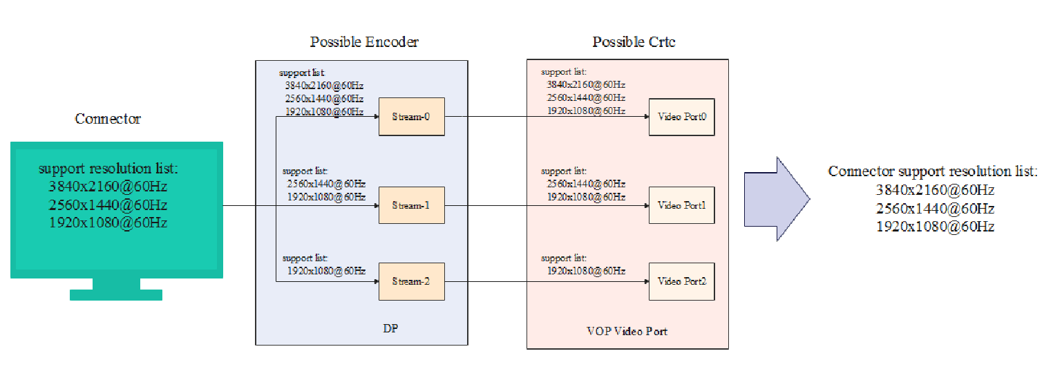
Because DP streams and VOP Video Ports have different capabilities, some resolutions cannot be output on particular paths. For example, 3840x2160@60Hz cannot display normally on Video Port2 -> DP Stream-2.
Userspace must therefore limit resolutions for the selected display path, or the connected display’s maximum resolution must not exceed the capability of DP Stream-2.