
RM182XMC0 is the RK182X M.2 Key M AI-coprocessor family: RM1820MC0 and RM1828MC0. This article organises the supplied two-page Rev1.0 brief’s specifications, performance table, power, figures and ordering data for ArmSoM-platform evaluation. Source measurements are not ArmSoM tests.
Download the original two-page M.2 brief
1. Models and compute
| Ordering model | Chip | Built-in DRAM | Source positioning | Interface |
|---|---|---|---|---|
| RM1820MC0 | RK1820 | 2.5GB | 3B | M.2 Key M, PCIe2.1 |
| RM1828MC0 | RK1828 | 5GB | 7B | M.2 Key M, PCIe2.1 |
The rating is20TOPS@INT8 with INT4/INT8/INT16/FP8/FP16/BF16. The Chinese brief describes built-in DRAM as having “hundreds of GB” high bandwidth without an explicit per-second unit, exact number or test conditions. No GB/s figure is invented here. Model size alone does not establish quantisation, context length or runtime memory suitability.
2. Listed models and software
The list names Qwen2.5 0.5B/1.5B/3B, Qwen3 0.6B/1.7B, FastVLM, MobilnetV1, MobilnetV2, Resnet50V2, yolov5s, yolov6s, yolov8s. Mobilnet preserves the source spelling. Qwen2.5 7B appears separately in the performance table despite being absent from that list; both are retained.
Software comprises development-host RKNN3 Toolkit, board-side RKNN3 Runtime and RKNN3 Model Zoo conversion/deployment examples. The brief gives no exact versions, installation commands, host OS matrix or quantisation configuration. Obtain matching packages and documentation for deployment.
3. Source performance and power
Both modes specify Input tokens: 128. TTFT is time to first token; TPS is generation rate. Values below reproduce the source.
| Model | Mode | TTFT (ms) | TPS (tokens/s) | Average power (W) | Peak power (W) |
|---|---|---|---|---|---|
| Qwen2.5 3B | Power-saving | 144.455 | 54.537 | 5.35 | 15.14 |
| Qwen2.5 3B | Standard | 96.05 | 77.945 | 7.2 | 24.86 |
| Qwen2.5 7B | Power-saving | 288.255 | 35.044 | 7.02 | 16.11 |
| Qwen2.5 7B | Standard | 186.435 | 51.476 | 10.4 | 27.28 |
Host, firmware, quantisation, output length, sampling, cooling and power-measurement boundaries are not fully disclosed. These figures do not promise speed for arbitrary3B/7B models; average power is not peak supply demand.
4. Power and host wiring
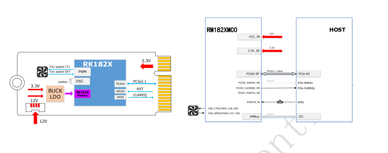
An additional12V input is required alongside M.2-slot3.3V. The diagram connects PCIe0 EP to host RC through PCIe2.1 x1, with CLKREQ, optional WAKE, RESETN_IN/0Ω, optional SMBus/I2C, and fan PWM/tachometer. Key M does not make this an NVMe SSD or guarantee arbitrary-slot power/software compatibility.
5. Mechanical clearance
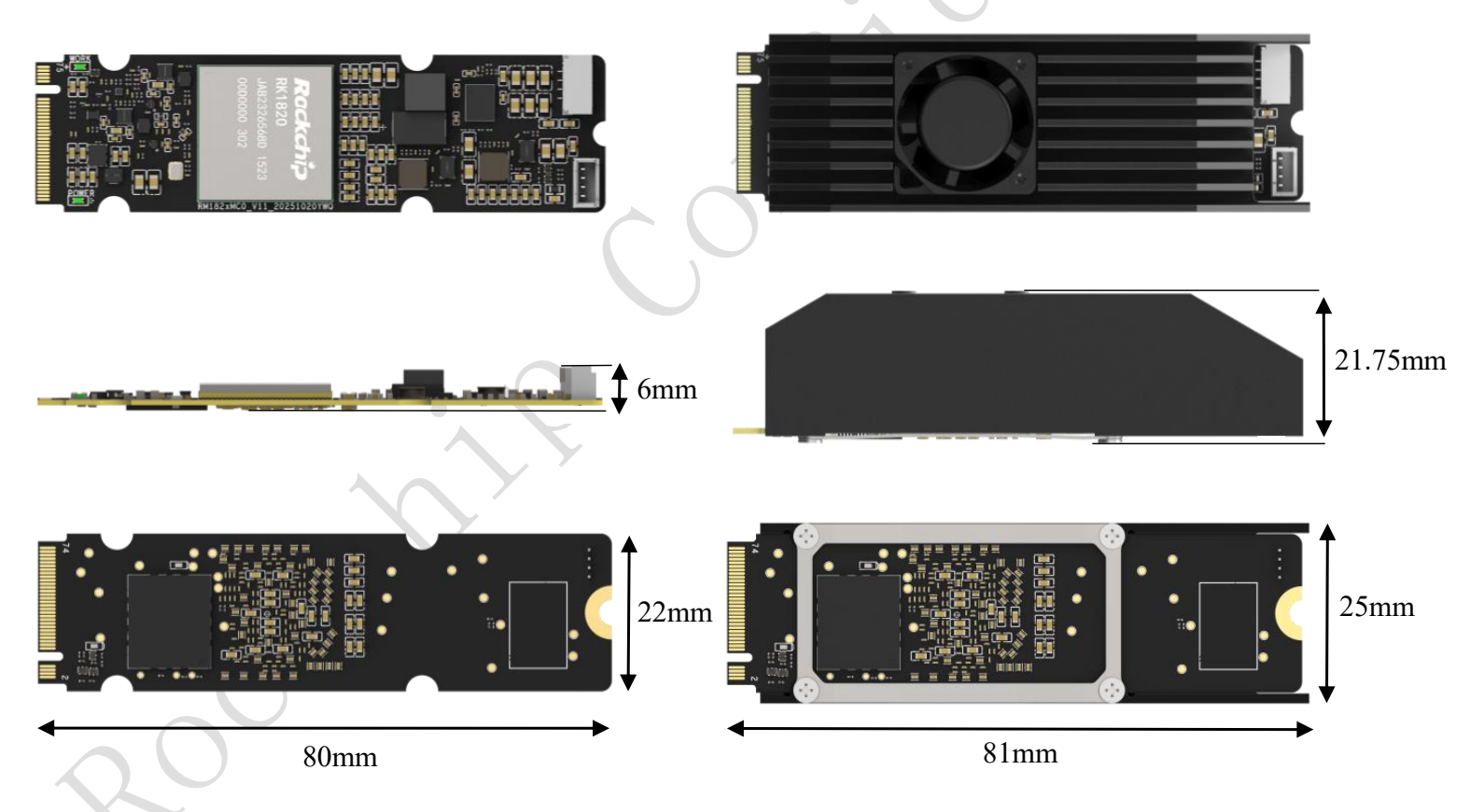
The bare module is22×80mm with6mm marked in side view. The cooled assembly is marked81mm long, 25mm wide and21.75mm high. Allow for wiring, mounting and airflow beyond the2280 board outline. This illustration is not a complete manufacturing-tolerance drawing.
6. Difference from SO-DIMM
M.2 ordering codes are RM1820MC0/RM1828MC0; SO-DIMM codes are RM1820SA0/RM1828SA0. A shared chip family does not imply matching interfaces, power, mechanics or firmware. Do not transfer the SO-DIMM8–14.4V range, 260-pin definitions or thermal limits to M.2 without confirmation.
7. ArmSoM evaluation sequence
Confirm host RC and slot wiring → verify3.3V, additional12V and peak margin → check cooling clearance → match driver, firmware and RKNN3 → validate accuracy, TTFT/TPS and stability. These PDFs alone do not establish direct support on any particular ArmSoM board; validate the actual hardware revision.