
ArmSoM platform reference: complete technical content of the manufacturer RK Firmware Upgrade Failure Analysis 1.2. The sole source is a 25-page Chinese PDF; English, Russian and German are full translations and all four use 45 original figures. Tool logs, binary comparisons, PCB and waveform evidence remain in original screenshots; unclear characters are not guessed. Readable batch code and the final power table are additionally transcribed. Examples cover several older SoCs/tools, not tested ArmSoM boards. Verify actual hardware, BSP, memory datasheet and boot chain.
Scope and source checks
- These are vendor troubleshooting heuristics, not proof that a single message identifies a failed component. Preserve logs, verify firmware/power, then inspect evidence. Rework and chip replacement require qualified facilities.
- Repair, IDB erasure, reflashing and misc writes can destroy data or boot state. Back up and verify exact targets/partition sizes. Secure-boot devices need matching signed firmware, not bypassing verification.
- Pin38-to-VCC,10K pull-ups and EXT CSD179/167/162 apply only to matching parts/platforms. Source spellings RTS_n, DATO and RK3329 are explicitly flagged; never infer wiring or SoC identity from a likely typo.
- FLASH ID tables cover historical common values, not all modern parts. The trailing separator after D3 does not identify a second value; none is invented. Interpret00/FF only in the source diagnostic context, not as a substitute for electrical testing.
- Page25 is an image-only power table, retained and transcribed row by row: Ta=25°C at3.3V, VCC2.7V–3.6V and60mV peak-to-peak ripple. The body100-300mA/100-700uA ranges are not identical guarantees to this single-model example.
- The third batch-code screenshot on page17 is already clipped on the right in the PDF. Its full command can be recovered from the preceding screenshot and explicit-RK29→-RK30 change; both originals remain. Dates/times within logs remain technical context; cover dates, contact and revision table are removed. No flashing, erasing, register changes or hardware operations were performed.
1. Overview
Factories and engineers frequently encounter firmware-upgrade failures. This guide collects common problems and diagnostic suggestions. Tools continue to evolve, so exact messages may differ, while messages for the same failure type should be similar.
2. Common failures and analysis
2.1. Boot Code download failure
Message in the production tool:
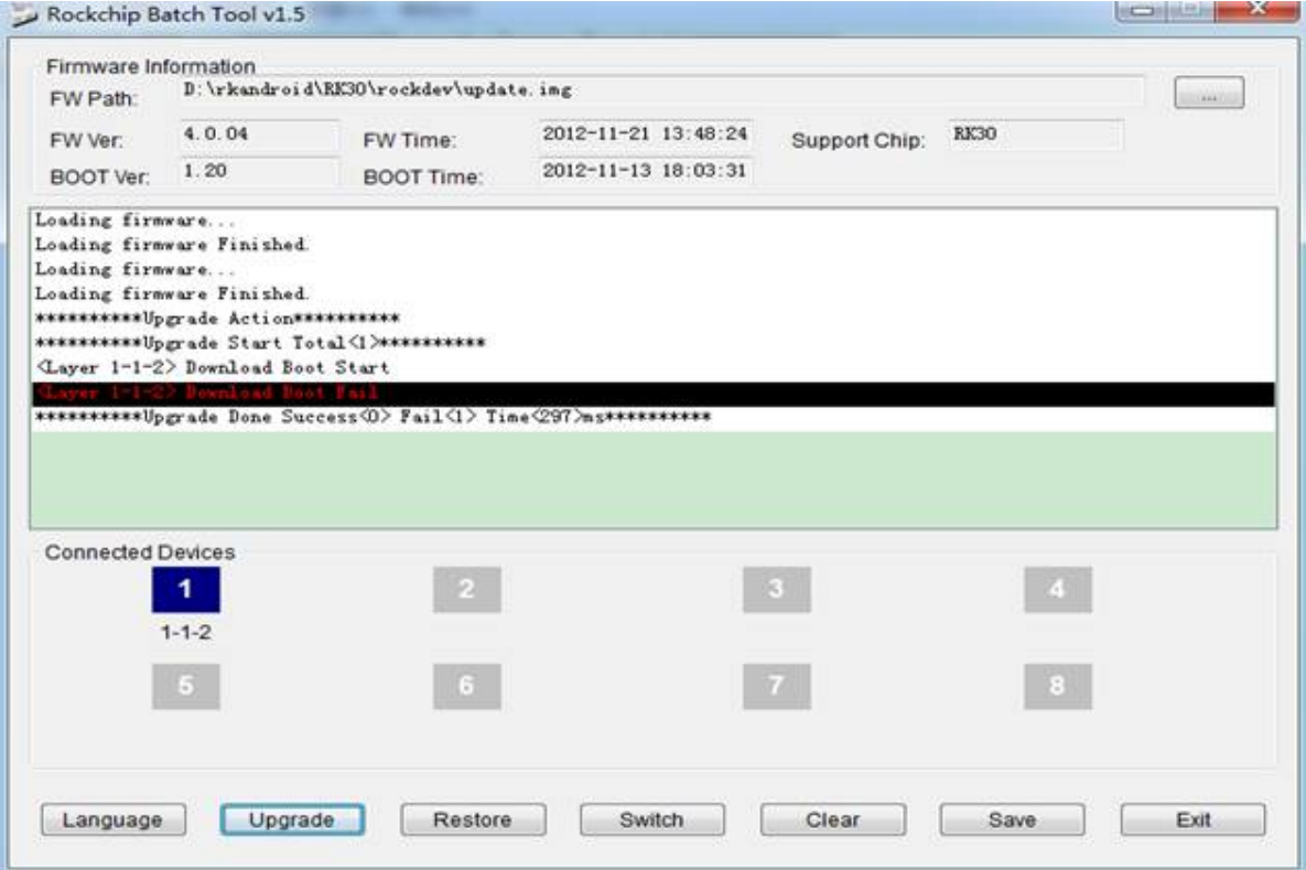
Message in the development tool:
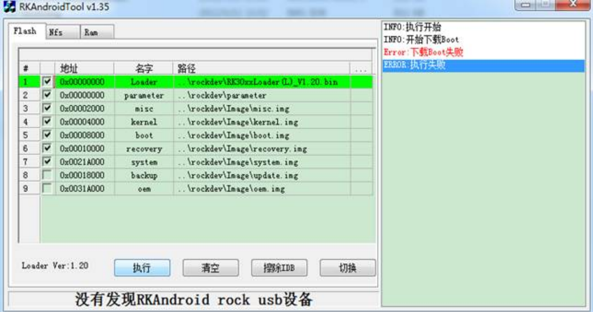
Log file in the production tool’s log directory:
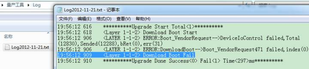
Log file in the development tool’s log directory:
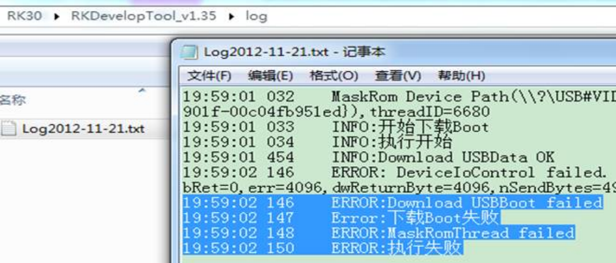
Possible causes:
-
Poor USB signal quality.
-
Poor SoC solder joints or power problems.
-
DDR-related problems.
-
Insufficient power supply.
-
Unsigned firmware used on a secure-boot-enabled device.
Diagnostic steps:
-
Use the DDR test tool to check for solder-joint problems.
-
Use a short, good-quality USB 2.0 cable connected to a rear PC USB port for upgrading.
-
Check whether USB-line ESD components are present and correctly specified.
-
Check USB supply voltage and ripple.
-
Check whether USB traces run parallel to other traces on adjacent layers.
-
Check resistor and capacitor values around the SoC and USB circuitry.
-
Use the board’s supported external supply or battery.
-
Secure-boot devices require the corresponding correctly signed firmware.
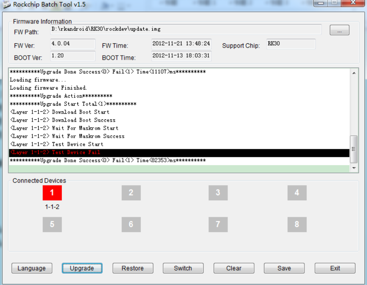
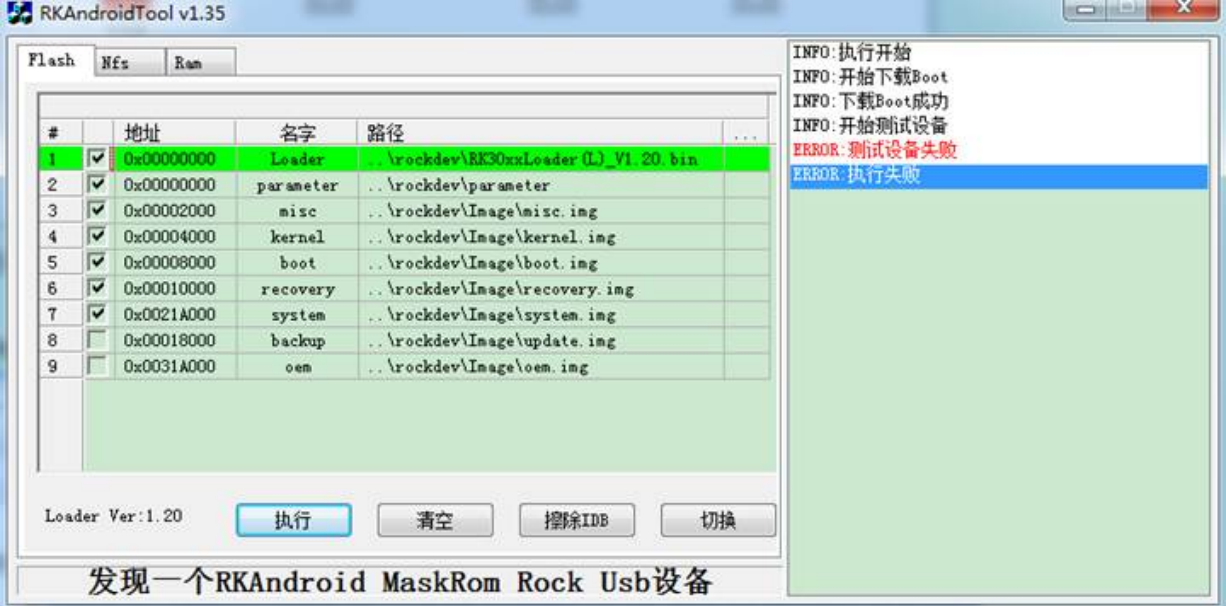
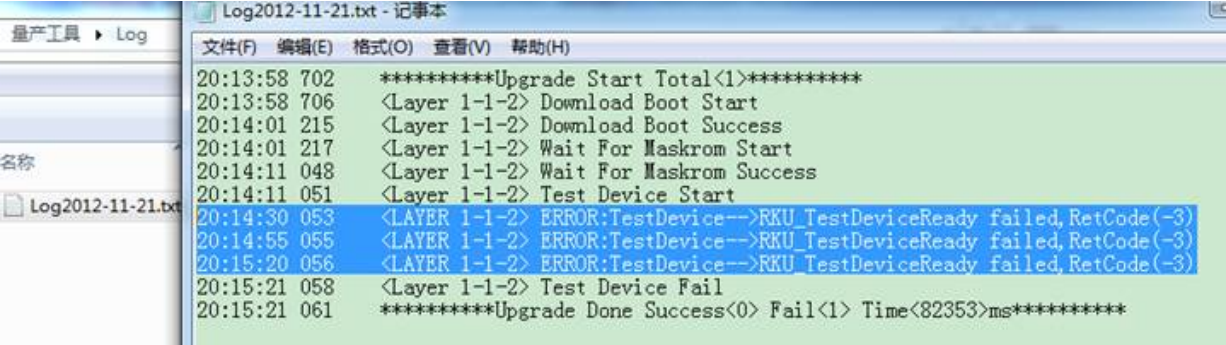
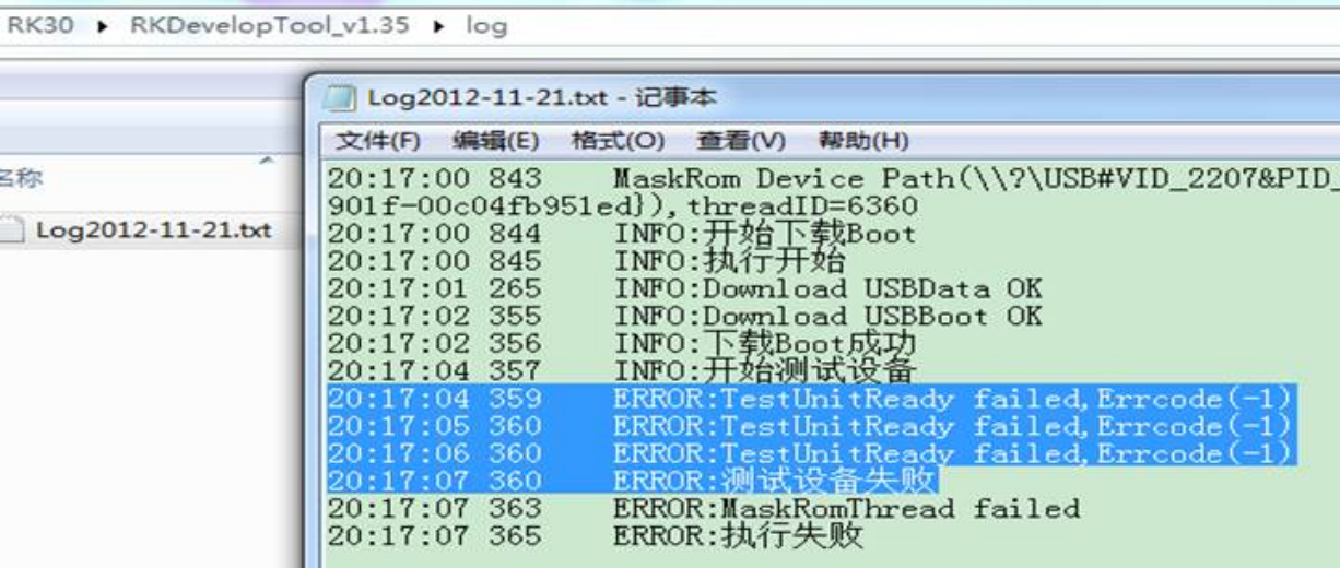
2.2. Device test fails after successful Boot Code download
Production-tool message:
Development-tool message:
Production-tool log:
Development-tool log:
Possible causes:
-
DDR components or DDR PCB routing; the source considers these relatively likely.
-
Poor USB signal quality.
-
Wrong usbplug used when packaging miniloader under U-Boot.
Diagnostic steps:
-
Test DDR soldering with the DDR test tool.
-
Review DDR PCB routing for layout-rule violations.
-
Replace the DDR component if warranted by diagnosis.
-
For USB checks, follow section 2.1.
-
Connect the serial console and determine whether the CPU reaches DDR initialization or usbplug.
2.3. IDB preparation: NAND FLASH or EMMC soldering problems
Production tool reports IDB preparation failure:
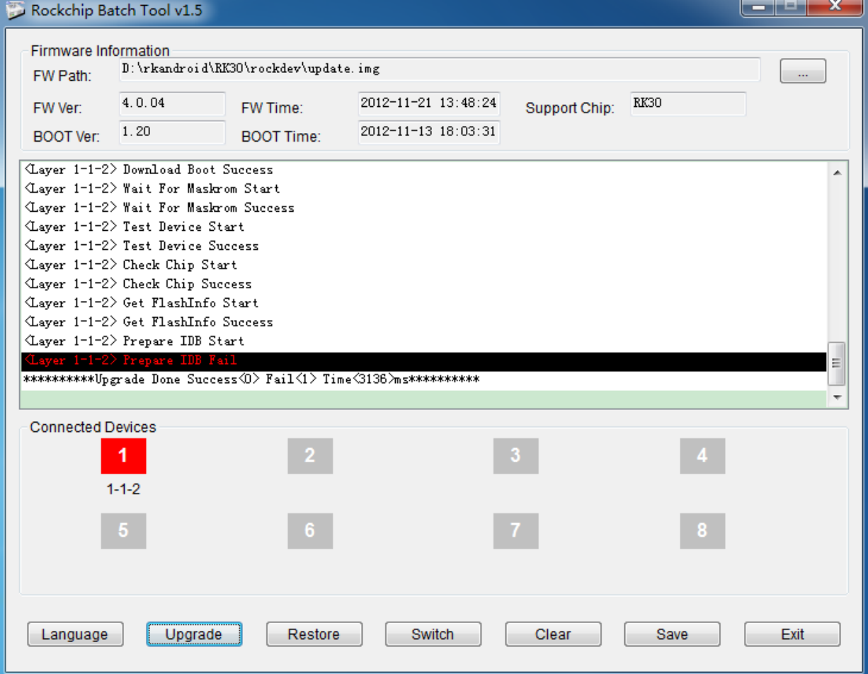
Production-tool log:
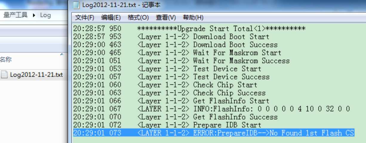
Development tool reports failure to write ID_BLOCK:
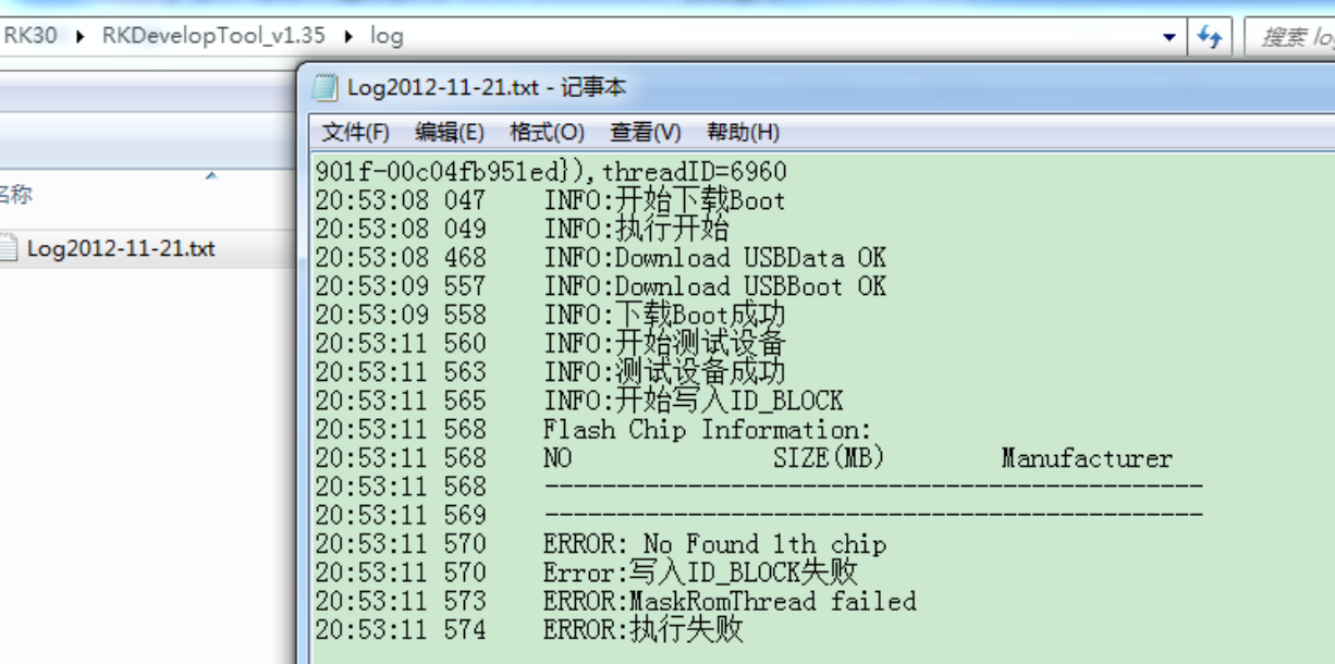
The development-tool log says NAND FLASH was not found and ID_BLOCK writing failed.
Possible causes:
-
Poor NAND FLASH/EMMC solder joints.
-
Unsupported NAND FLASH.
-
PCB defects.
-
Incorrect FLASH VCCQ supply.
-
Incorrect FLASH SEL selection at the AP.
-
Missing CMD and D0 pull-ups for EMMC.
Diagnostic steps:
-
Rework NAND FLASH/EMMC soldering and inspect the PCB, using qualified board-repair procedures.
-
Compare schematic and NAND datasheet, especially pin 38. The source says most Toshiba, Sandisk and Samsung parts require VCC there, with no such requirement for other parts. This is a historical generalization: the exact part’s datasheet and package are authoritative.
-
For unsupported NAND, obtain an appropriate driver update through the vendor’s support channel and inspect its NAND support list to confirm the actual part.
-
Use serial logs to help diagnose soldering. A normal NAND device prints FLASH IDs as below. An EMMC device normally does not print FLASH IDs in this source’s boot path.
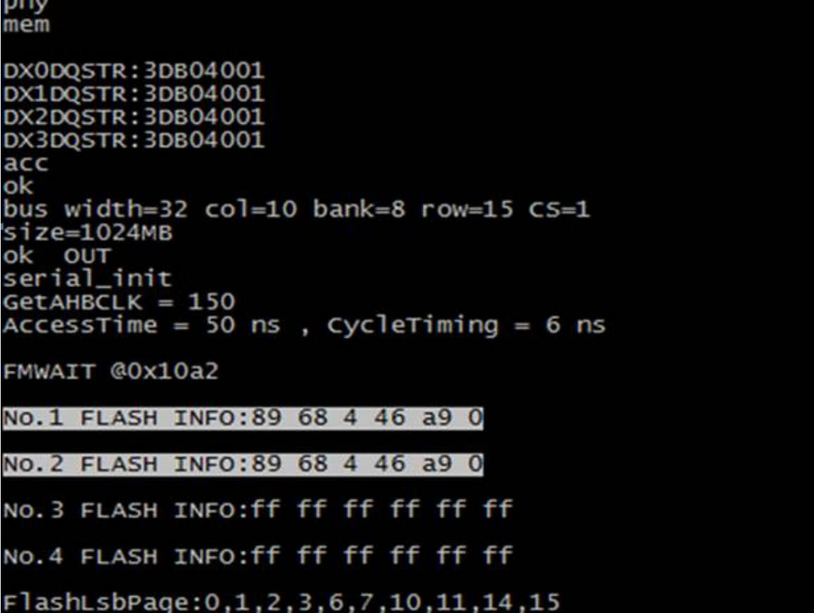
The first FLASH ID byte identifies the manufacturer:
| ID | Manufacturer |
|---|---|
| 2C | Micron |
| AD | Hynix |
| 45 | Sandisk |
| 89 | Intel |
| EC | Samsung |
| 98 | Toshiba |
| 00 | No NAND FLASH connected |
| FF | No NAND FLASH connected |
| Other values | Poor soldering or unsupported NAND FLASH. |
The second byte indicates capacity; common source values follow:
| ID | Capacity |
|---|---|
| 75 | 32MB |
| 76 | 64MB |
| 78、79、F1、D1 | 128MB |
| DA、71 | 256MB |
| DC | 512MB |
| D3、 | 1GB |
| D5、48 | 2GB |
| D7、68 | 4GB |
| D9、88、DE、3A、64 | 8GB |
| 3C、A8、84 | 16GB |
| Other values | Poor soldering or unsupported NAND FLASH. |
Diagnostic examples:
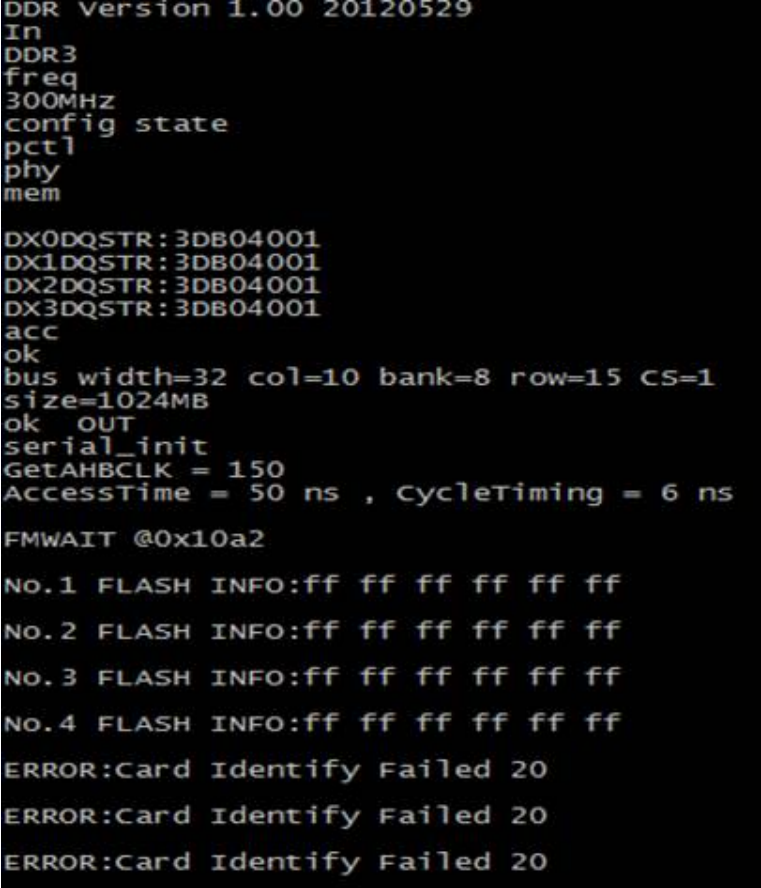
- The log below is attributed by the source to poor NAND FLASH or EMMC soldering.
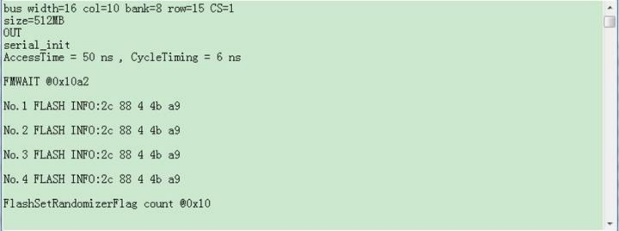
- Only two NAND chips are fitted, but the system detects four. The source attributes this to faulty NAND chip-select (CS) soldering.
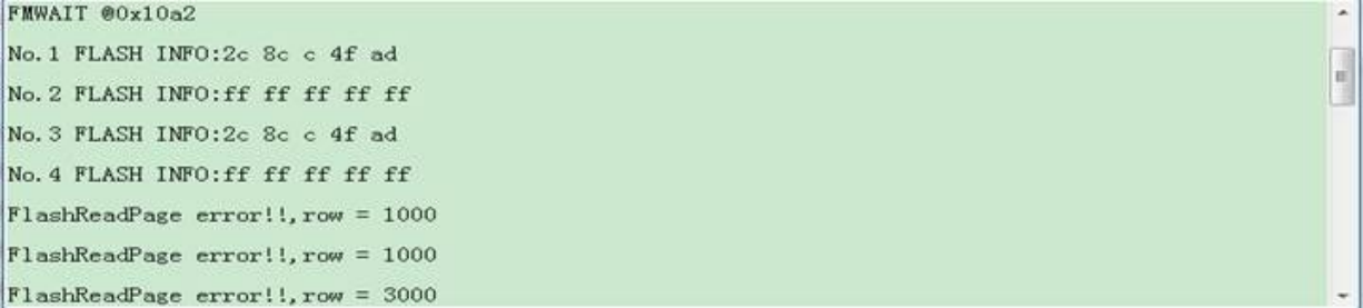
- Two NAND chips are fitted and detected, but their IDs are wrong. First byte 2c identifies Micron. The second byte is 8C instead of the expected 88 for this example; the source concludes a soldering fault. Do not treat every unlisted ID as faulty without checking the exact part.
2.4. IDB writing failure
Production tool reports ID_BLOCK writing failure:
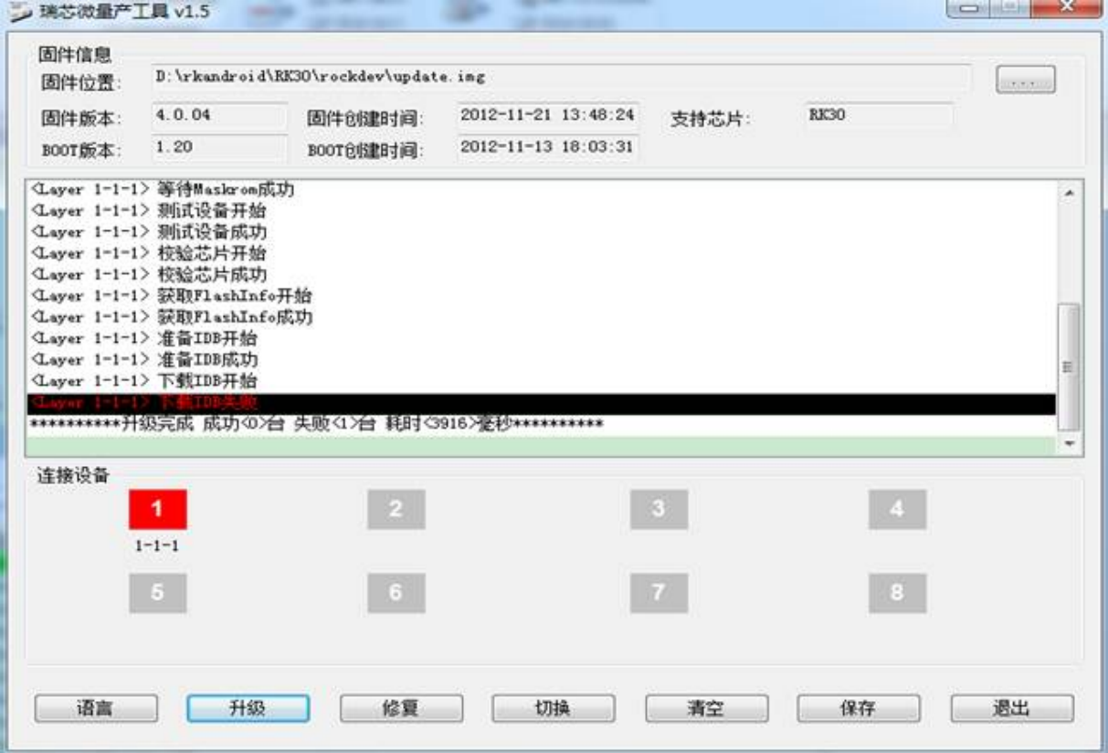
Development-tool ID_BLOCK writing failure:
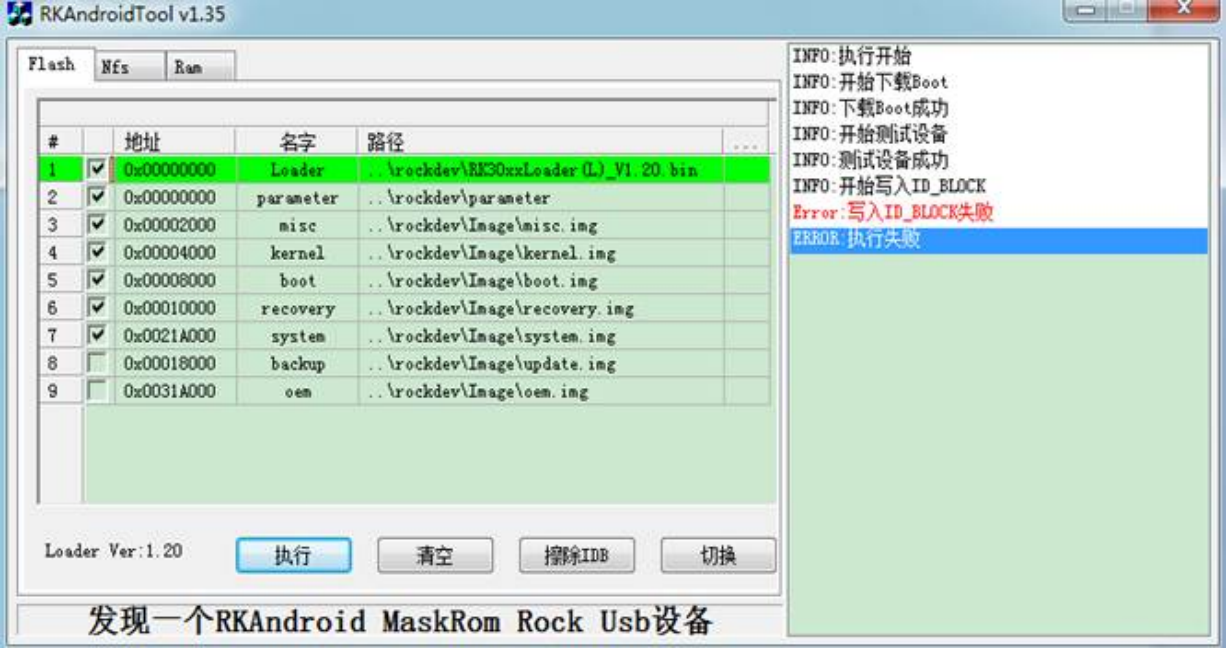
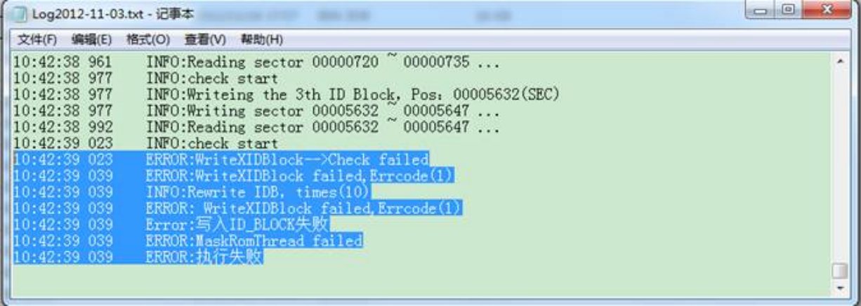
The development-tool log reports a comparison mismatch:
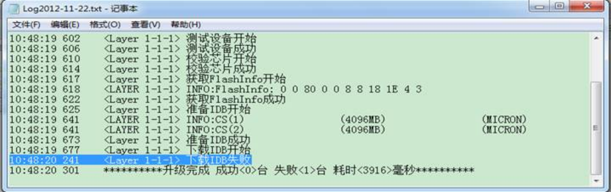
Production-tool log:
Several binary files also appear in the LOG directory:
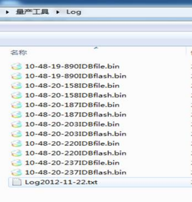
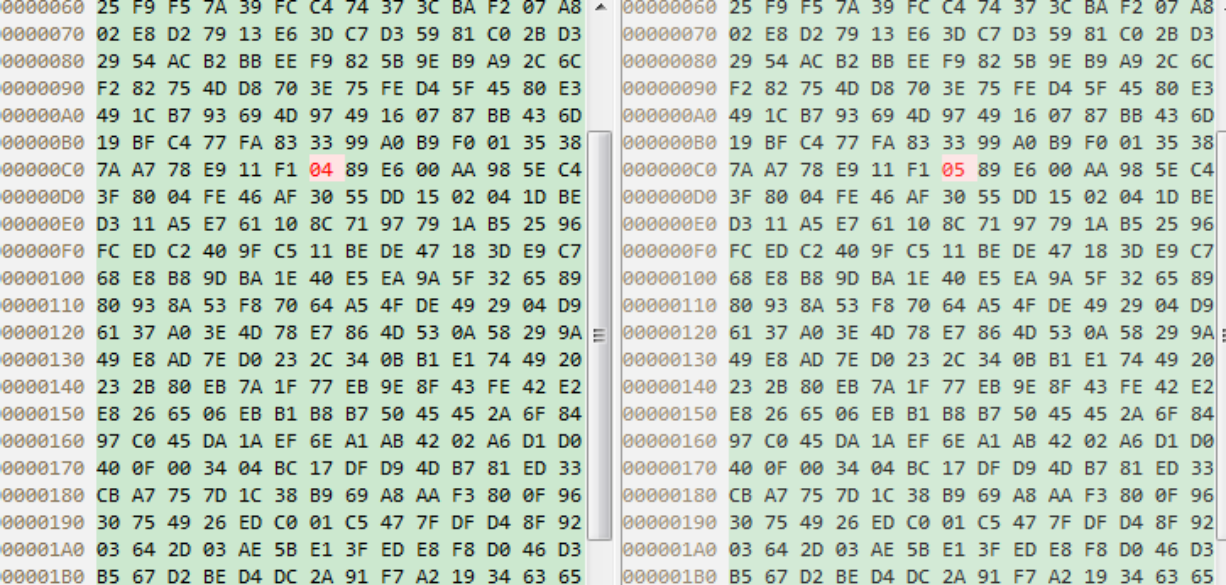
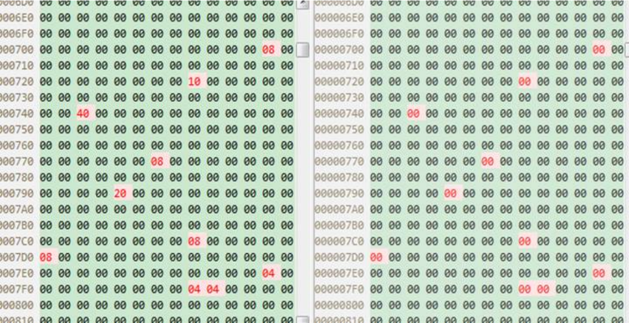
Use a binary comparison tool on files with the same prefix and the suffixes “flash” and “file”, for example:

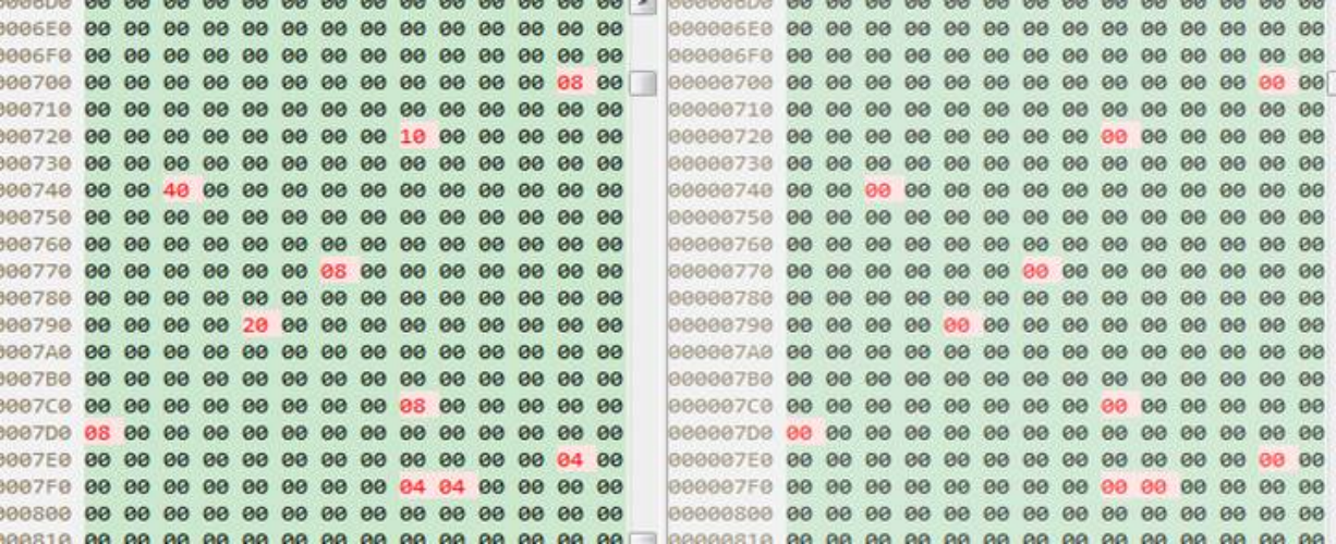
In the example below, one or a few differing bits suggest DDR trouble. Follow section 2.2; this is a diagnostic clue, not proof by itself.
Many differing bits usually indicate NAND trouble in the source’s examples. It suggests retrying the upgrade. Excessive NAND supply ripple or missing filter capacitors can cause the same symptom. If the power is normal and repeated upgrades do not resolve it, replace NAND after confirming the diagnosis.
2.5. Firmware download failure
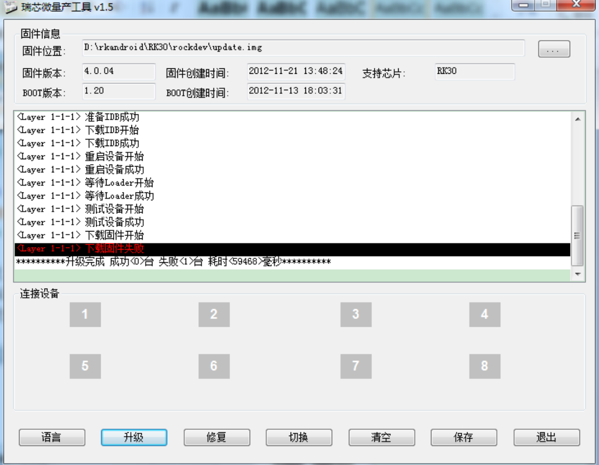
Production tool reports firmware download failure:
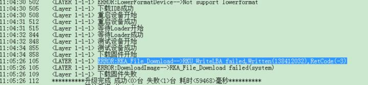
Production-tool log: WriteLBA failed, error code (-3).
Production-tool log: ReadLBA failed, error code (-4).
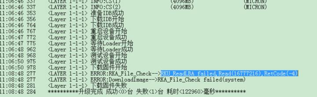
The source attributes both cases to interrupted USB communication. Use section 2.1’s checks.
Production-tool log: RKA_File_Check failed.
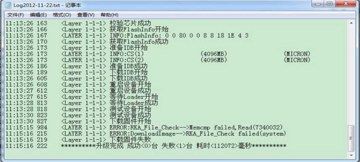
The log directory also contains two files: intended firmware data and incorrect data read back from flash.
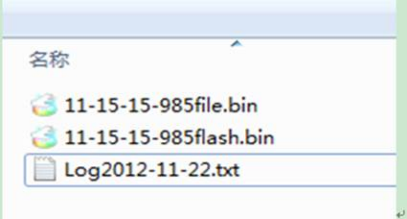
Compare the two files. One or a few differing bits suggest DDR trouble; follow section 2.2.
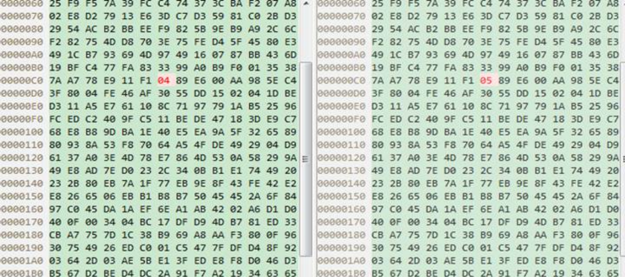

For many differing bits, the source suspects NAND and proposes the production tool’s “Repair” mode or “Erase IDB” in the development tool before reflashing. These operations can destroy data and boot metadata: back up and verify the target first. The original button images are retained below.

Reflash only after the selected repair/erase step and the necessary checks.
Excessive NAND supply ripple or missing filter capacitors can cause this too. If supply checks and reflashing do not solve it, replace NAND after diagnosis.
Development-tool messages/logs are similar to the production tool, so apply the same analysis.
2.6. Chip verification failure
Production-tool chip verification usually fails when the selected firmware does not match the SoC. During development, the chip parameter used to package firmware may be wrong. The source says the development tool does not check chip information; wrong firmware may fail to boot or return to upgrade mode. Reflash the correct firmware.
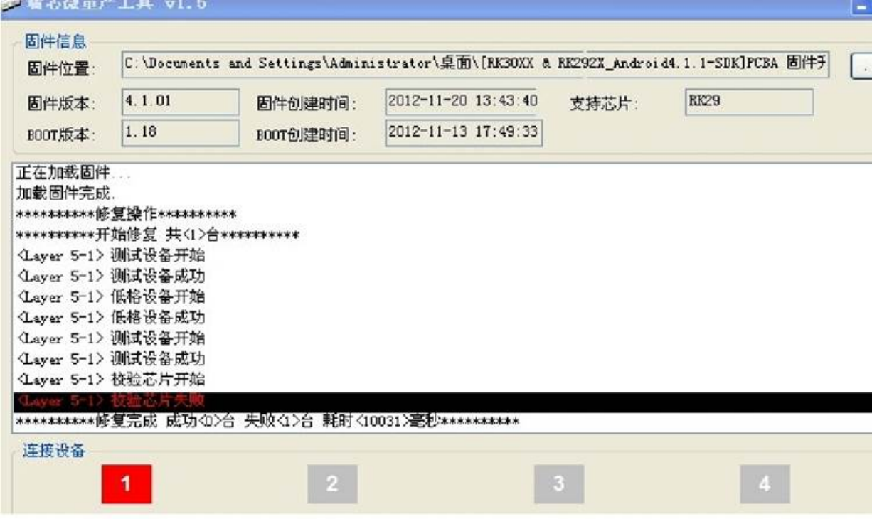
The example firmware is for RK30 but was incorrectly packaged as RK29. Open mkupdate.bat and correct the chip argument.
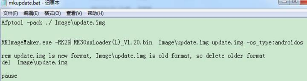
Afptool -pack ./ Image\update.img
RKImageMaker.exe -RK29 RK30xxLoader(L)_V1.20.bin Image\update.img update.img -os_type:androidos
rem update.img is new format, Image\update.img is old format, so delete older format
del Image\update.img
pause
Change the RKImageMaker.exe chip argument to -RK30 for this RK30 example.
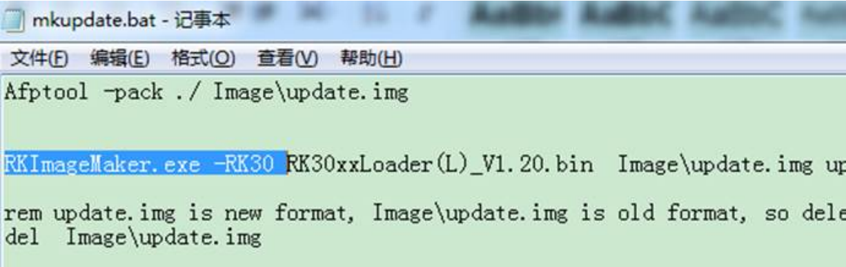
Afptool -pack ./ Image\update.img
RKImageMaker.exe -RK30 RK30xxLoader(L)_V1.20.bin Image\update.img update.img -os_type:androidos
rem update.img is new format, Image\update.img is old format, so delete older format
del Image\update.img
pause
For further configuration details, consult the documents in the firmware-generation tool directory.
3. Other problems
3.1. Still in upgrade mode after automatic reboot
Case 1: after flashing with the development tool, the device does not boot and appears in upgrade mode over USB. Serial output is shown below.
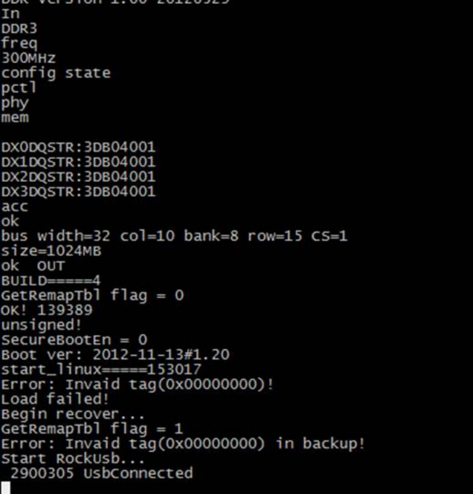
Readable key serial states (excerpt; the full log remains in the original image):
unsigned!
SecureBootEn = 0
Boot ver: 2012-11-13#1.20
Error: Invaid tag(0x00000000)!
Load failed!
Begin recover...
GetRemapTbl flag = 1
Error: Invaid tag(0x00000000) in backup!
Start RockUsb...
2900305 UsbConnected
The source attributes this case to flashing misc.img without flashing recovery.img.
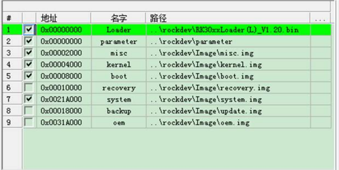
Remedy: reflash recovery.img. The source also describes writing another file larger than 32KB to misc to clear its commands; this is destructive and must not be applied blindly to modern layouts.
Case 2: the source lists RK3329 and RK3368 as examples that may fail to boot if trust.img was not flashed. Flash the matching trust.img. RK3329 is retained as written and requires platform verification.
3.2. EMMC devices do not boot at power-on
The source associates this mostly with RK3188, PX3, PX2, RK3066 and RK3168, after updating loader or assembling preprogrammed memory. Checks follow.
-
Inspect schematic/layout. CMD and DATA0-DATA7 require pull-ups; the source recommends 10K. Check their soldering. EMMC traces must not be routed through connections to NC pins.
-
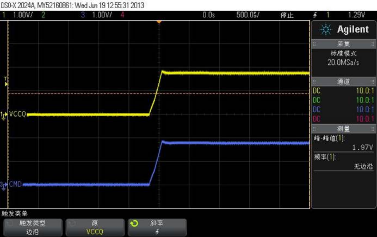
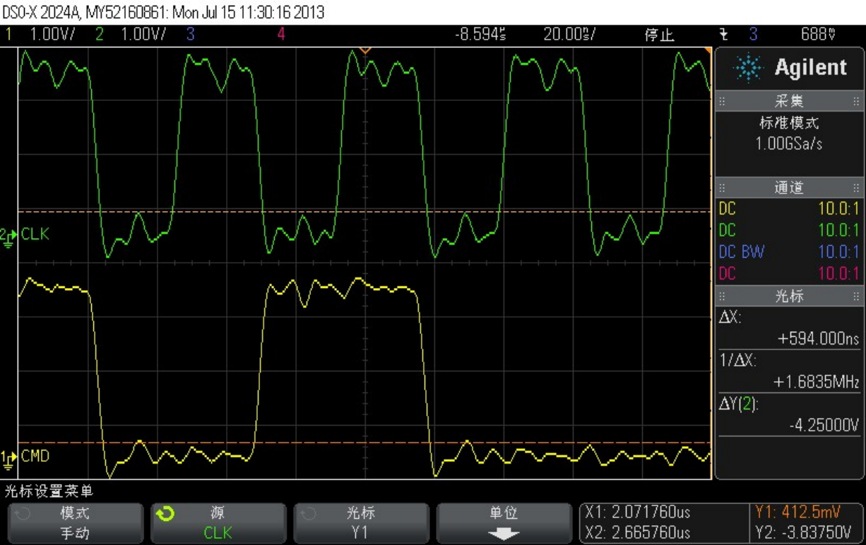
Measure power-up timing with an oscilloscope. CMD should rise with EMMC VCCQ, as shown. Some EMMC devices cannot boot if CMD rises later than VCCQ.
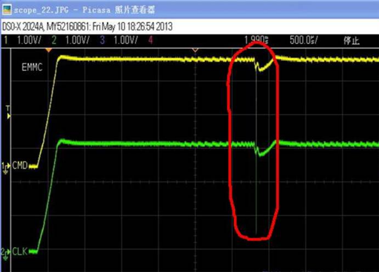
- Check CMD and CLK for glitches. Some EMMC devices fail to boot if glitches occur. The source observed this with RK3066 plus a TI PMU and proposes changing the power-up sequence.
- Check overshoot on CMD, CLK and DATA; series termination may help. Strong CLK ringing in the example may cause logic errors.
-
Check VCC ripple; consider appropriate filtering capacitors.
-
For preprogrammed memory, verify EXT CSD configuration.
Source EXT CSD settings: byte 179 = 0x08 (boot from boot1 without ACK); byte 167 = 0x1F; byte 162 = 0x01 (enable reset pin). Leave all other settings at defaults. These are platform-specific source values, not universal programming instructions; some settings may be irreversible.
For RK312X, RK3228, RK3366, RK3288 and RK3399, the source says remaining in MASKROM after flashing usually indicates one or more incorrectly connected EMMC D0-D7 lines.
3.3. EMMC device fails to boot after reset
Check that the SoC’s EMMC_PWEN connects to the EMMC pin called RTS_n in the source. Verify the actual schematic and datasheet signal name; do not infer a connection from this potentially misspelled label.
For preprogrammed firmware on RK3188, PX3, PX2, RK3066 or RK3168, the source requires EXTCSD byte 162 = 0x01.
3.4. Long delay before LOADER on EMMC
The source attributes the delay to BOOTROM entering NAND detection, which takes several seconds. Checks follow.
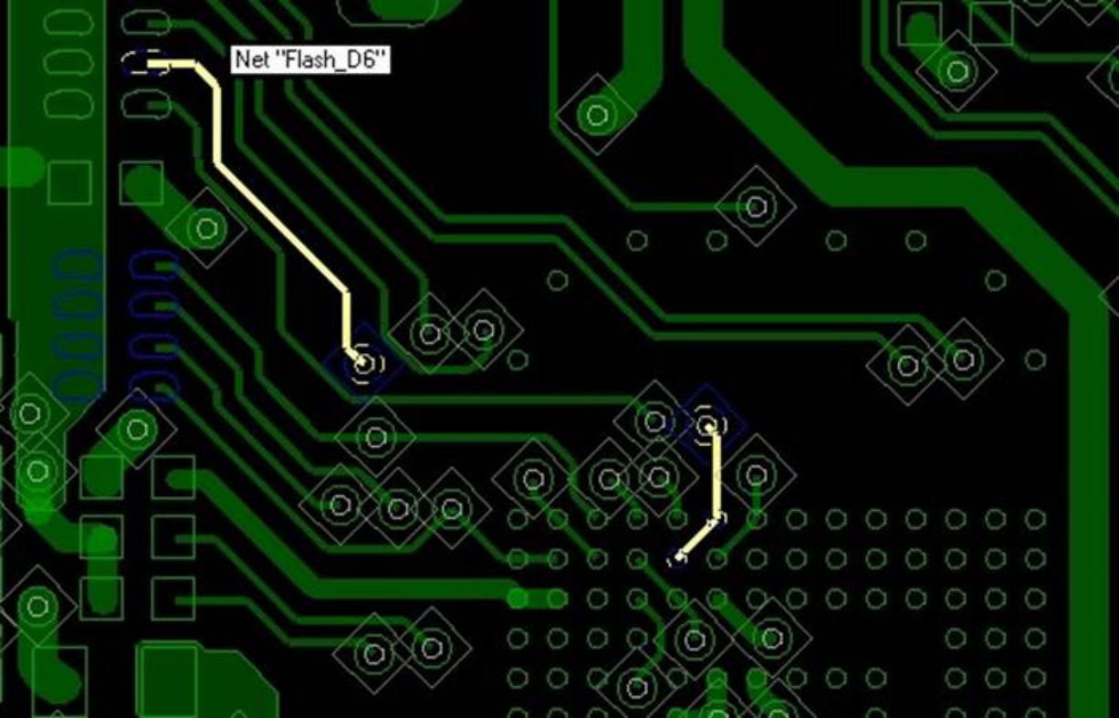
- Inspect schematic/layout, CMD and DATA0-DATA7 pull-ups (recommended 10K), and solder joints. Do not route EMMC signals through NC pins. The example PCB connects DATA6 through an NC pin and consequently boots slowly.
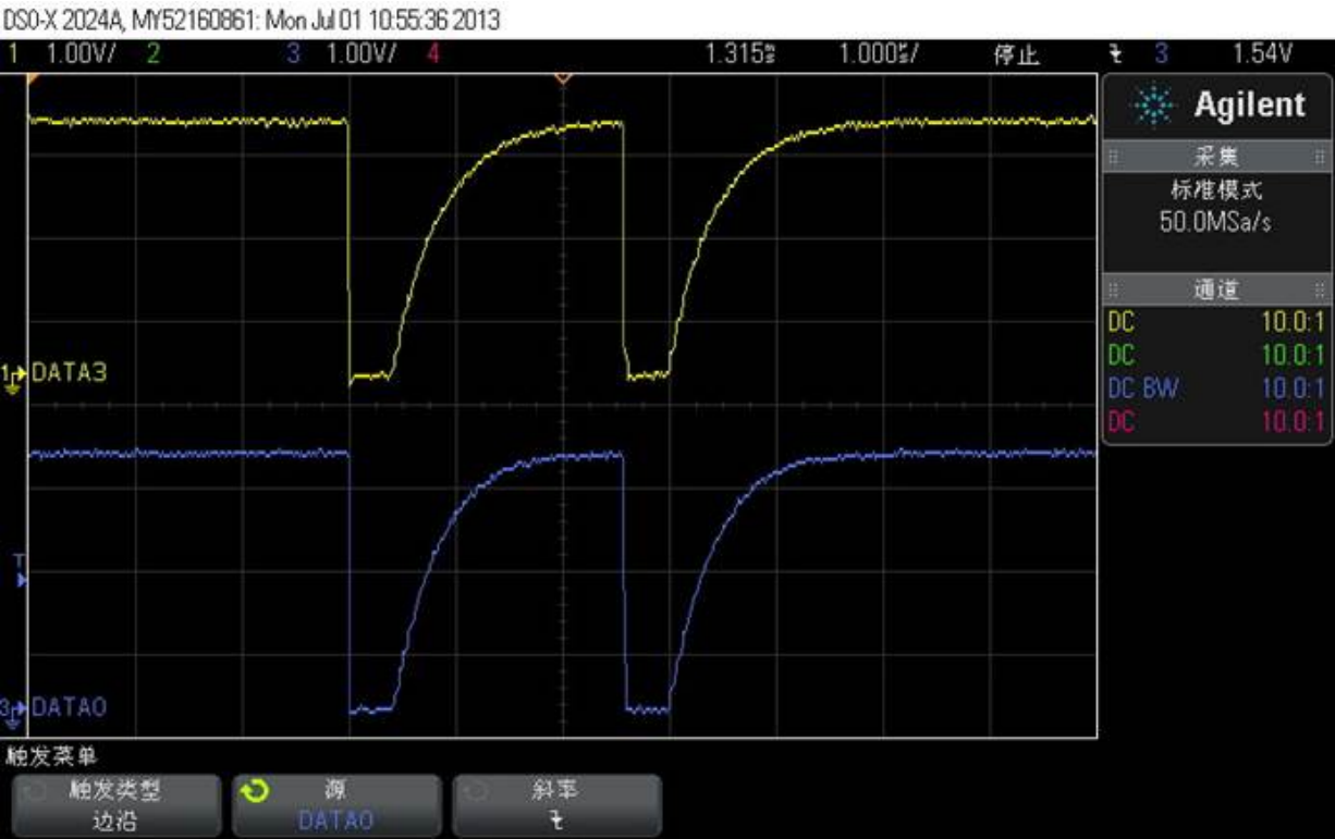
- Measure DATA0-DATA7 on power-up (the source spells the first signal DATO). DATA rise time must be less than 2us in this example. Figure 2 expands the red-ellipse region of Figure 1 to measure that rise time.
Figure 1:
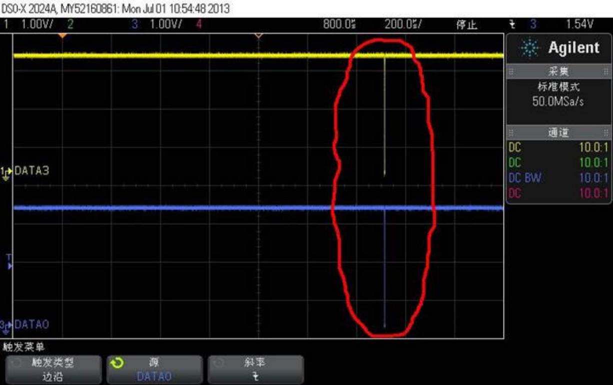
Figure 2: expanded rise-time waveform.
3.5. EMMC read/write errors while Android runs
Possible causes:
-
Insufficient VCC/VCCQ supply causing voltage collapse during operation.
-
Poor routing and severe interference.
Remedies:
- Check whether external activity such as Wi-Fi disturbs EMMC power; the source recommends a separate supply.
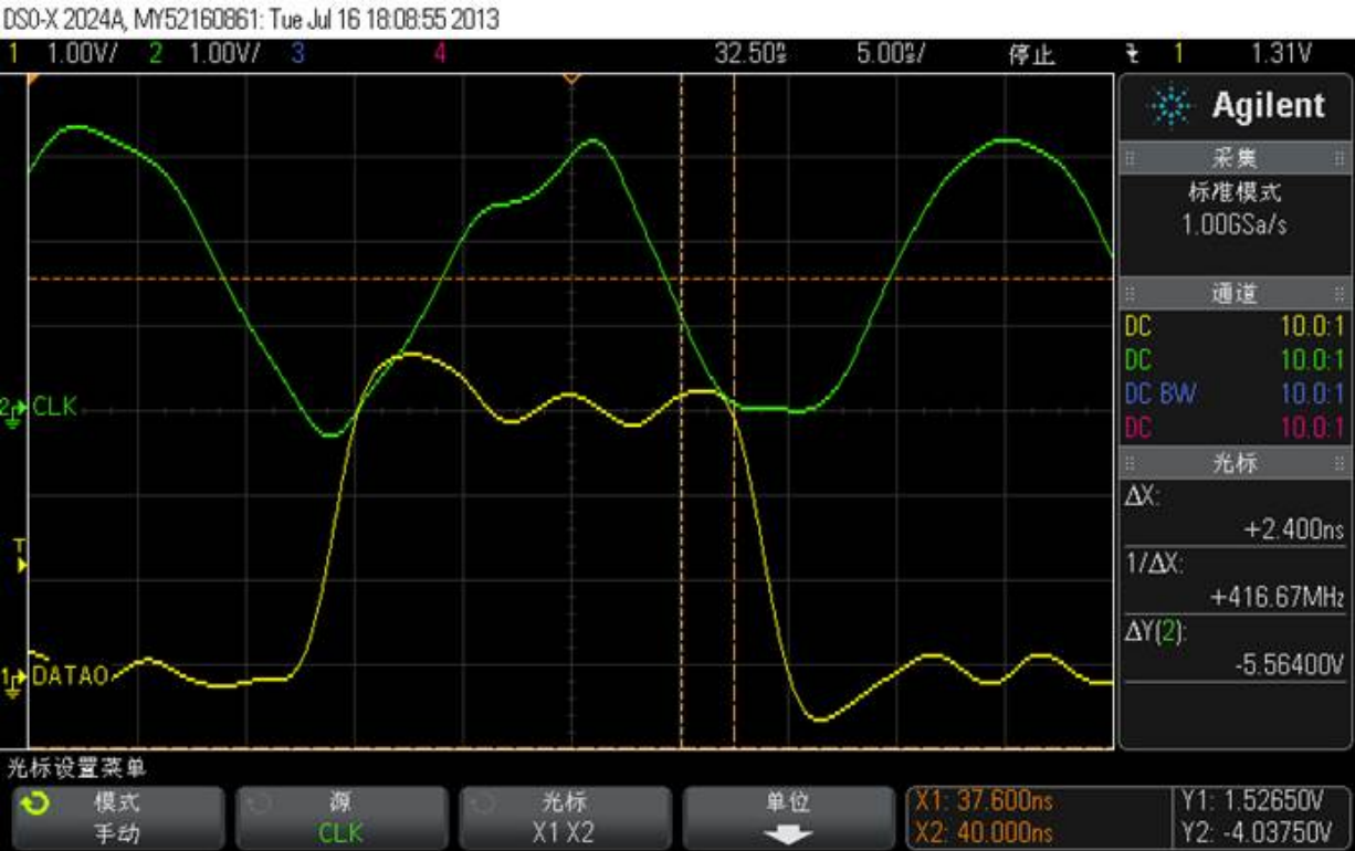
- Measure bus timing with an oscilloscope. The example shows insufficient hold time at the falling CLK edge in DDR mode, which may cause logic errors.
3.6. EMMC power consumption
The source quotes 100-300mA while reading/writing and 100-700uA in standby. Consumption depends on speed mode, EMMC frequency/capacity, interface voltage, temperature, manufacturer process and pull-up resistance. The following is a typical example for one unspecified EMMC model, not a universal limit.
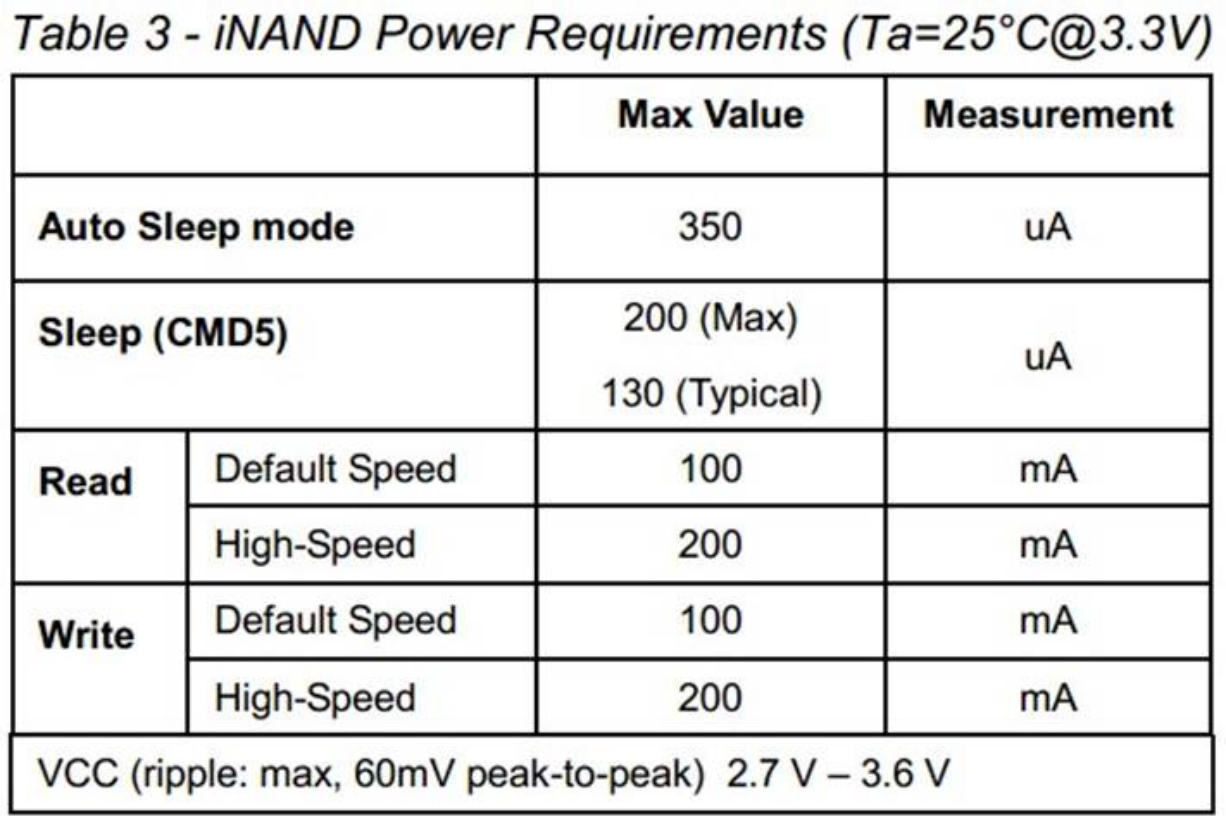
Ta=25°C @3.3V
| Mode | Maximum/typical value | Unit |
|---|---|---|
| Auto Sleep | 350 | uA |
| Sleep (CMD5) | 200 maximum;130 typical | uA |
| Read: default speed | 100 | mA |
| Read: high speed | 200 | mA |
| Write: default speed | 100 | mA |
| Write: high speed | 200 | mA |
VCC:2.7V–3.6V; maximum ripple60mV peak-to-peak.