
Chinese source V1.0.1, kernel scope 3.10 / 4.4 / 4.19. The technical preface introduces RK808 submodule concepts, functions, DTS configuration and troubleshooting; the full technical body is retained. No English PDF is available. All four languages use Chinese-PDF original figures, some already bearing English labels. Platform reference only: verify the actual ArmSoM PMIC, SoC, power tree, pins, SDK/BSP and kernel. Not a claim of support on every ArmSoM board; no hardware testing was performed.
Voltage, pin-mode and register writes can power off or damage hardware; these are unexecuted source examples. Source
0.737.5, differences between voltage/sequence tables,regulator-ramp-delay12500 versus example 6001, and the claimed four functions versus actual list count are retained without guessing corrections. Verify the pin-table default active-high INT versus active-low prose, VCC11 supply in the VCC10 row, OSC32KOUT type I and incomplete VCCA description against the datasheet. LDO7 sequence value 1.8/OFF omits V in the source.
1. Basics
1.1 Overview
RK808 is a high-performance PMIC integrating 4 high-current DCDCs, 8 LDOs, 2 SWITCH outputs, 1 RTC and adjustable power-up sequencing. System power rails are generally divided into DCDC and LDO types. Their general characteristics follow; consult further references for details.
-
DCDC: efficient at a large input/output voltage difference, but with relatively high ripple and cost; therefore used for large voltage drops and high-current loads. Two common modes are PWM, with good ripple/transient response but lower efficiency, and PFM, with higher efficiency but weaker load capability.
-
LDO: low efficiency at a large input/output voltage difference, but low cost. Optimize the system to improve conversion efficiency: for a 1.1V LDO output, its input can be supplied by the VCCIO_3.3V DCDC. Where the circuit permits, connect the LDO input to a DCDC output, taking power-up sequencing into account.
1.2 Functions
From the user perspective, RK808 functions are described as four parts:
-
regulator: controls the state of individual DCDC and LDO supplies.
-
rtc: provides clockkeeping, timing and related functions.
-
clk: two 32.768KHZ clock outputs; one is always on and cannot be controlled, while the other is software-controlled.
1.3 Pin functions
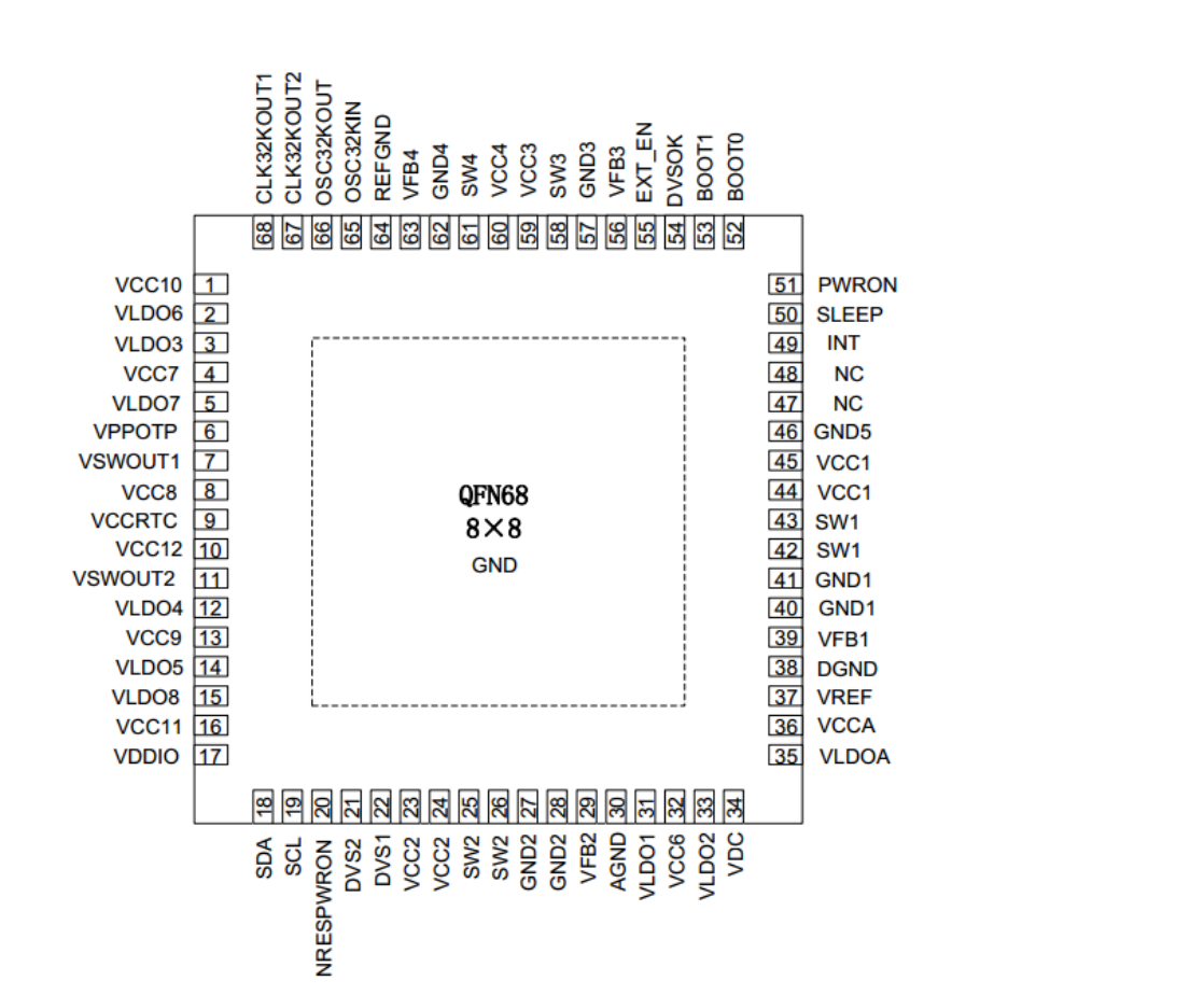
Chinese PDF original · p5
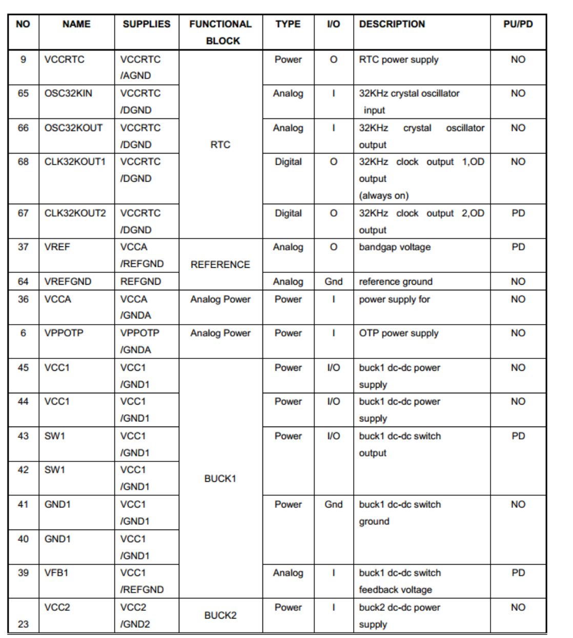
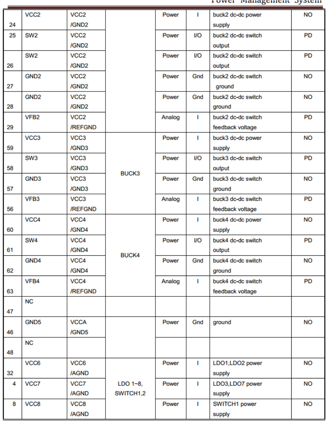
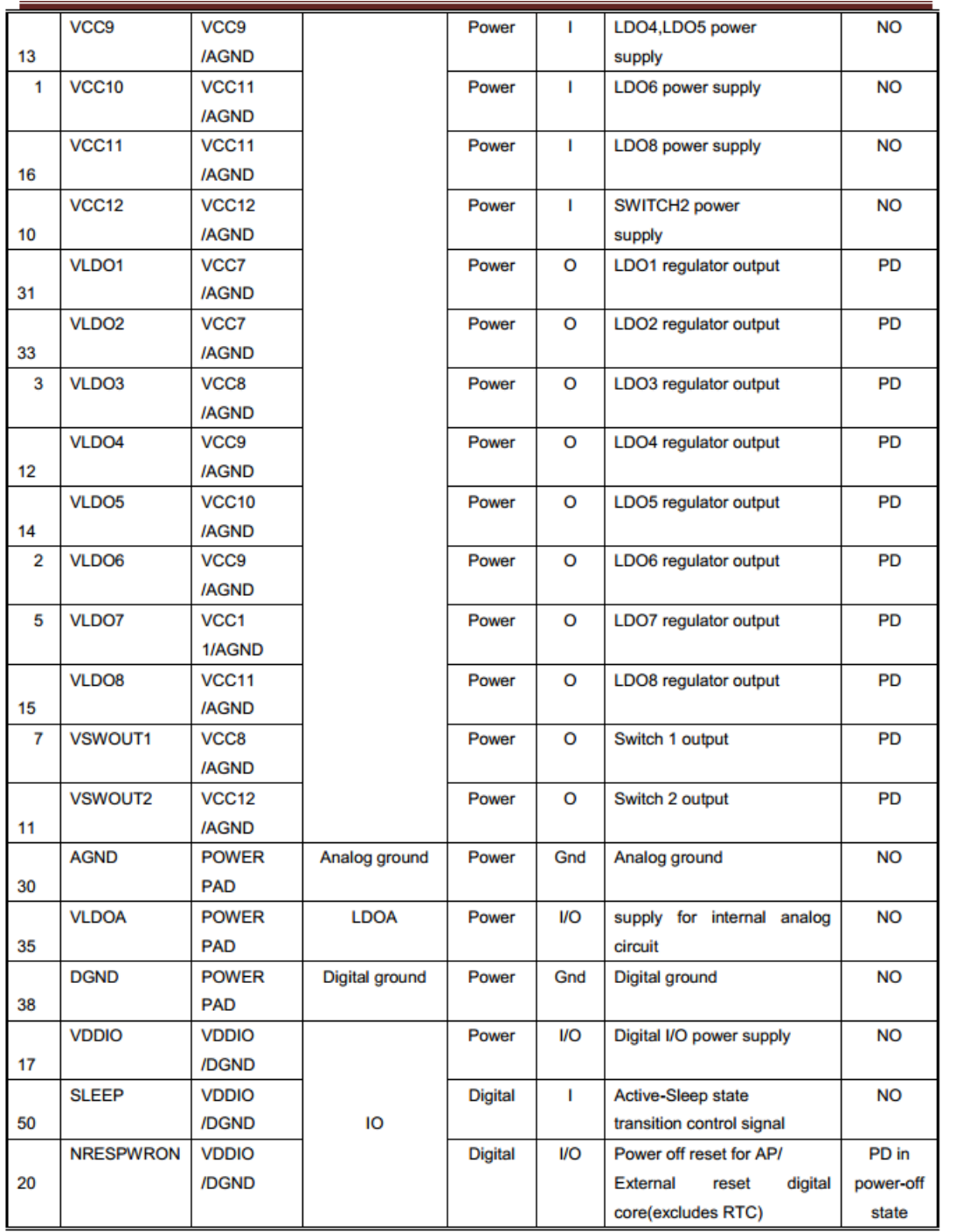
Pay particular attention to the SLEEP and INT pins in the following descriptions.
Chinese PDF original · p6
Chinese PDF original · p7
Chinese PDF original · p8
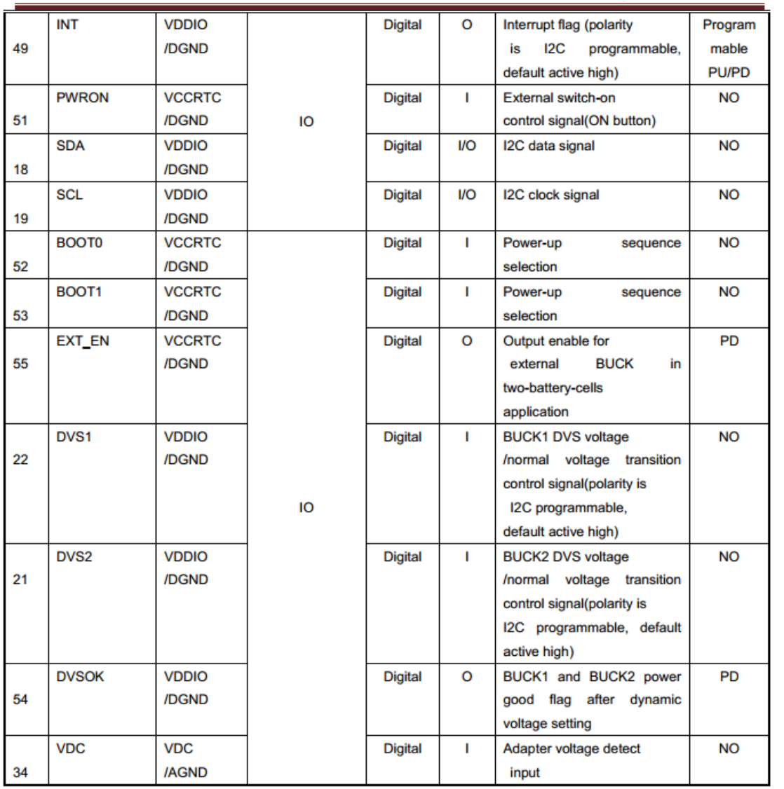
Chinese PDF original · p9
Editable transcription of the original tables above.
| Pin no. | Name | Supplies | Functional block | Type | I/O | Description | PU/PD |
|---|---|---|---|---|---|---|---|
| 9 | VCCRTC | VCCRTC/AGND | RTC | Power | O | RTC power supply | NO |
| 65 | OSC32KIN | VCCRTC/DGND | RTC | Analog | I | 32KHz crystal oscillator input | NO |
| 66 | OSC32KOUT | VCCRTC/DGND | RTC | Analog | I | 32KHz crystal oscillator output | NO |
| 68 | CLK32KOUT1 | VCCRTC/DGND | RTC | Digital | O | 32KHz clock output 1, open drain, always on | NO |
| 67 | CLK32KOUT2 | VCCRTC/DGND | RTC | Digital | O | 32KHz clock output 2, open drain | PD |
| 37 | VREF | VCCA/REFGND | REFERENCE | Analog | O | Bandgap voltage | PD |
| 64 | VREFGND | REFGND | REFERENCE | Analog | Gnd | Reference ground | NO |
| 36 | VCCA | VCCA/GNDA | Analog Power | Power | I | Power supply for (source incomplete) | NO |
| 6 | VPPOTP | VPPOTP/GNDA | Analog Power | Power | I | Power supply of OTP | NO |
| 45 | VCC1 | VCC1/GND1 | BUCK1 | Power | I/O | Power supply of BUCK1 DC-DC | NO |
| 44 | VCC1 | VCC1/GND1 | BUCK1 | Power | I/O | Power supply of BUCK1 DC-DC | NO |
| 43 | SW1 | VCC1/GND1 | BUCK1 | Power | I/O | BUCK1 DC-DC switch output | PD |
| 42 | SW1 | VCC1/GND1 | BUCK1 | Power | I/O | BUCK1 DC-DC switch output | PD |
| 41 | GND1 | VCC1/GND1 | BUCK1 | Power | Gnd | Ground | NO |
| 40 | GND1 | VCC1/GND1 | BUCK1 | Power | Gnd | Ground | NO |
| 39 | VFB1 | VCC1/REFGND | BUCK1 | Analog | I | Output feedback voltage of BUCK1 DC-DC switch | PD |
| 23 | VCC2 | VCC2/GND2 | BUCK2 | Power | I | Power supply of BUCK2 DC-DC | NO |
| 24 | VCC2 | VCC2/GND2 | BUCK2 | Power | I | Power supply of BUCK2 DC-DC | NO |
| 25 | SW2 | VCC2/GND2 | BUCK2 | Power | I/O | BUCK2 DC-DC switch output | PD |
| 26 | SW2 | VCC2/GND2 | BUCK2 | Power | I/O | BUCK2 DC-DC switch output | PD |
| 27 | GND2 | VCC2/GND2 | BUCK2 | Power | Gnd | Ground | NO |
| 28 | GND2 | VCC2/GND2 | BUCK2 | Power | Gnd | Ground | NO |
| 29 | VFB2 | VCC2/REFGND | BUCK2 | Analog | I | Output feedback voltage of BUCK2 DC-DC switch | PD |
| 59 | VCC3 | VCC3/GND3 | BUCK3 | Power | I | Power supply of BUCK3 DC-DC | NO |
| 58 | SW3 | VCC3/GND3 | BUCK3 | Power | I/O | BUCK3 DC-DC switch output | PD |
| 57 | GND3 | VCC3/GND3 | BUCK3 | Power | Gnd | Ground | NO |
| 56 | VFB3 | VCC3/REFGND | BUCK3 | Analog | I | Output feedback voltage of BUCK3 DC-DC switch | PD |
| 60 | VCC4 | VCC4/GND4 | BUCK4 | Power | I | Power supply of BUCK4 DC-DC | NO |
| 61 | SW4 | VCC4/GND4 | BUCK4 | Power | I/O | BUCK4 DC-DC switch output | PD |
| 62 | GND4 | VCC4/GND4 | BUCK4 | Power | Gnd | Ground | NO |
| 63 | VFB4 | VCC4/REFGND | BUCK4 | Analog | I | Output feedback voltage of BUCK4 DC-DC switch | PD |
| 47 | NC | ||||||
| 46 | GND5 | VCCA/GND5 | LDO1–8, SWITCH1,2 | Power | Gnd | Ground | NO |
| 48 | NC | ||||||
| 32 | VCC6 | VCC6/AGND | LDO1–8, SWITCH1,2 | Power | I | Power supply of LDO1,LDO2 | NO |
| 4 | VCC7 | VCC7/AGND | LDO1–8, SWITCH1,2 | Power | I | Power supply of LDO3,LDO7 | NO |
| 8 | VCC8 | VCC8/AGND | LDO1–8, SWITCH1,2 | Power | I | Power supply of SWITCH1 | NO |
| 13 | VCC9 | VCC9/AGND | LDO1–8, SWITCH1,2 | Power | I | Power supply of LDO4,LDO5 | NO |
| 1 | VCC10 | VCC11/AGND | LDO1–8, SWITCH1,2 | Power | I | Power supply of LDO6 | NO |
| 16 | VCC11 | VCC11/AGND | LDO1–8, SWITCH1,2 | Power | I | Power supply of LDO8 | NO |
| 10 | VCC12 | VCC12/AGND | LDO1–8, SWITCH1,2 | Power | I | Power supply of SWITCH2 | NO |
| 31 | VLDO1 | VCC7/AGND | LDO1–8, SWITCH1,2 | Power | O | LDO1 regulator output | PD |
| 33 | VLDO2 | VCC7/AGND | LDO1–8, SWITCH1,2 | Power | O | LDO2 regulator output | PD |
| 3 | VLDO3 | VCC8/AGND | LDO1–8, SWITCH1,2 | Power | O | LDO3 regulator output | PD |
| 12 | VLDO4 | VCC9/AGND | LDO1–8, SWITCH1,2 | Power | O | LDO4 regulator output | PD |
| 14 | VLDO5 | VCC10/AGND | LDO1–8, SWITCH1,2 | Power | O | LDO5 regulator output | PD |
| 2 | VLDO6 | VCC9/AGND | LDO1–8, SWITCH1,2 | Power | O | LDO6 regulator output | PD |
| 5 | VLDO7 | VCC11/AGND | LDO1–8, SWITCH1,2 | Power | O | LDO7 regulator output | PD |
| 15 | VLDO8 | VCC11/AGND | LDO1–8, SWITCH1,2 | Power | O | LDO8 regulator output | PD |
| 7 | VSWOUT1 | VCC8/AGND | LDO1–8, SWITCH1,2 | Power | O | SWITCH1 output | PD |
| 11 | VSWOUT2 | VCC12/AGND | LDO1–8, SWITCH1,2 | Power | O | SWITCH2 output | PD |
| 30 | AGND | POWER PAD | Analog ground | Power | Gnd | Analog ground | NO |
| 35 | VLDOA | POWER PAD | LDOA | Power | I/O | Supply for internal analog circuit | NO |
| 38 | DGND | POWER PAD | Digital ground | Power | Gnd | Digital ground | NO |
| 17 | VDDIO | VDDIO/DGND | IO | Power | I/O | Digital I/O supply | NO |
| 50 | SLEEP | VDDIO/DGND | IO | Digital | I | Active/sleep transition control signal | NO |
| 20 | NRESPWRON | VDDIO/DGND | IO | Digital | I/O | Power-off reset for AP / external reset of digital core (excluding RTC) | PD in power-off state |
| 49 | INT | VDDIO/DGND | IO | Digital | O | Interrupt flag; polarity programmable by I2C, default active high | Programmable PU/PD |
| 51 | PWRON | VCCRTC/DGND | IO | Digital | I | External switch-on control (ON button) | NO |
| 18 | SDA | VDDIO/DGND | IO | Digital | I/O | I2C data signal | NO |
| 19 | SCL | VDDIO/DGND | IO | Digital | I/O | I2C clock signal | NO |
| 52 | BOOT0 | VCCRTC/DGND | IO | Digital | I | Power-up sequence selection | NO |
| 53 | BOOT1 | VCCRTC/DGND | IO | Digital | I | Power-up sequence selection | NO |
| 55 | EXT_EN | VCCRTC/DGND | IO | Digital | O | Output enable for external BUCK in two-battery-cell application | PD |
| 22 | DVS1 | VDDIO/DGND | IO | Digital | I | BUCK1 DVS/normal-voltage transition; I2C-programmable polarity, default active high | NO |
| 21 | DVS2 | VDDIO/DGND | IO | Digital | I | BUCK2 DVS/normal-voltage transition; I2C-programmable polarity, default active high | NO |
| 54 | DVSOK | VDDIO/DGND | IO | Digital | O | BUCK1/BUCK2 power-good flag after dynamic voltage setting | PD |
| 34 | VDC | VDC/AGND | IO | Digital | I | Adapter-voltage detection input | NO |
1.4 Important concepts
I2C address: 7-bit slave address 0x1b. The PMIC has three operating modes.
-
PMIC normal mode: during normal system operation the PMIC is in normal mode and pmic_sleep is low.
-
PMIC sleep mode: the PMIC enters sleep to reduce its own consumption when the system suspends. Usually some outputs are reduced or disabled, configurable for the product. Raising pmic_sleep during standby enters sleep; when the SoC wakes, pmic_sleep returns low and the PMIC exits sleep.
-
PMIC shutdown mode: during system shutdown, the PMIC powers down the entire system. The AP configures pmic_sleep for shutdown over I2C, then raises pmic_sleep to enter shutdown.
pmic_sleep pin:
Normally low, keeping the PMIC in normal mode; raising it switches to sleep or shutdown.
pmic_int: normally high; an interrupt drives it low, and it stays low until the interrupt is handled.
pmic_pwron: connect the hardware power key to this pin; the driver detects press/release through it.
DCDC modes: besides PWM (force PWM) and PFM, AUTO dynamically switches between PWM and PFM. The PMIC supports PWM and AUTO PWM/PFM. AUTO has higher efficiency but poorer ripple/transient response. For stability, use PWM during operation and switch to AUTO PWM/PFM during suspend.
DCDC3 voltage: this special rail cannot change voltage through registers; external divider resistors set it. Change the external hardware to change voltage. Rockchip designs generally use it for VCC_DDR.
Runtime voltage adjustment ranges of DCDC and LDO:
- Continuous DCDC voltage ranges:
| Voltage range (V) | Step (mV) | Voltage settings (V) |
|---|---|---|
| 0.7125 ~ 1.45 | 12.5 | 0.7125、0.725、0.737.5、 ……、1.45 |
| 1.8 ~ 3.3 | 100 | 1.8、1.9、2.0、2.2….、3.3 |
- Continuous LDO voltages:
| Voltage range (V) | Step (mV) | Voltage settings (V) |
|---|---|---|
| 0.8 ~ 3.4 | 100 | 0.8、0.9、1.0、1.1、1.2、 …… 3.4 |
1.5 Power-on conditions and sequence
- Power-on conditions: any one of the following powers on the PMIC:
- EN transitions from low to high.
- EN remains high and an RTC alarm interrupt occurs.
- EN remains high and the PWRON key is pressed.
- Power-up sequencing: SoC platforms can require different rail sequences. The current sequences are shown below; consult the latest applicable datasheet for specifics.
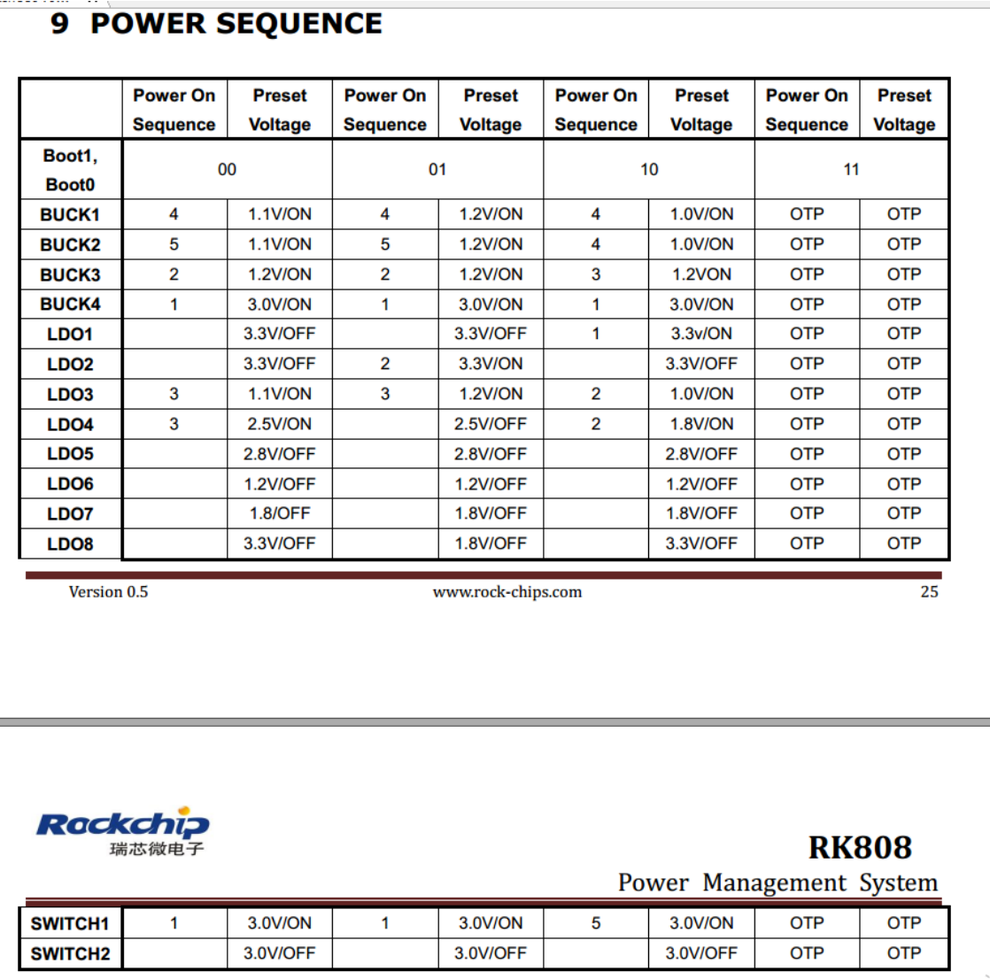
Chinese PDF original · p11
Sequence table transcribed from the original image; blanks, x, OTP and ON/OFF are retained.
| Rail | 00 Sequence | 00 Default voltage | 01 Sequence | 01 Default voltage | 10 Sequence | 10 Default voltage | 11 Sequence | 11 Default voltage |
|---|---|---|---|---|---|---|---|---|
| BUCK1 | 4 | 1.1V/ON | 4 | 1.2V/ON | 4 | 1.0V/ON | OTP | OTP |
| BUCK2 | 5 | 1.1V/ON | 5 | 1.2V/ON | 4 | 1.0V/ON | OTP | OTP |
| BUCK3 | 2 | 1.2V/ON | 2 | 1.2V/ON | 3 | 1.2V/ON | OTP | OTP |
| BUCK4 | 1 | 3.0V/ON | 1 | 3.0V/ON | 1 | 3.0V/ON | OTP | OTP |
| LDO1 | 3.3V/OFF | 3.3V/OFF | 1 | 3.3V/ON | OTP | OTP | ||
| LDO2 | 3.3V/OFF | 2 | 3.3V/ON | 3.3V/OFF | OTP | OTP | ||
| LDO3 | 3 | 1.1V/ON | 3 | 1.2V/ON | 2 | 1.0V/ON | OTP | OTP |
| LDO4 | 3 | 2.5V/ON | 2.5V/OFF | 2 | 1.8V/ON | OTP | OTP | |
| LDO5 | 2.8V/OFF | 2.8V/OFF | 2.8V/OFF | OTP | OTP | |||
| LDO6 | 1.2V/OFF | 1.2V/OFF | 1.2V/OFF | OTP | OTP | |||
| LDO7 | 1.8/OFF | 1.8V/OFF | 1.8V/OFF | OTP | OTP | |||
| LDO8 | 3.3V/OFF | 1.8V/OFF | 3.3V/OFF | OTP | OTP | |||
| SWITCH1 | 1 | 3.0V/ON | 1 | 3.0V/ON | 5 | 3.0V/ON | OTP | OTP |
| SWITCH2 | 3.0V/OFF | 3.0V/OFF | 3.0V/OFF | OTP | OTP |
2. Configuration
2.1 Drivers and menuconfig
2.1.1 3.10 kernelConfiguration
RK808 driver files:
drivers/mfd/rk808.c
drivers/mfd/rk808-irq.c
drivers/rtc/rtc-rk808.c
Reference RK808 DTS file:
arch/arm/boot/dts/rk808.dtsi
arch/arm/boot/dts/rk3288-evb-android-rk808-edp.dts
Corresponding menuconfig symbols:
CONFIG_MFD_RK808
CONFIG_RTC_RK808
2.1.2 4.4 kernelConfiguration
RK808 driver files:
drivers/mfd/rk808.c
drivers/rtc/rtc-rk808.c
drivers/regulator/rk808-regulator.c
drivers/clk/clk-rk808.c
Reference RK808 DTS file:
arch/arm64/boot/dts/rockchip/rk3399-evb-rev3.dtsi
Corresponding menuconfig symbols:
CONFIG_MFD_RK808
CONFIG_RTC_RK808
CONFIG_REGULATOR_RK808
CONFIG_COMMON_CLK_RK808
2.1.3 4.19 kernelConfiguration
RK808 driver files:
drivers/mfd/rk808.c
drivers/rtc/rtc-rk808.c
drivers/regulator/rk808-regulator.c     // 跟4.4内核不同
drivers/clk/clk-rk808.c
Corresponding menuconfig symbols:
CONFIG_MFD_RK808
CONFIG_RTC_RK808
CONFIG_REGULATOR_RK808
CONFIG_COMMON_CLK_RK808
2.2 DTS configuration
2.2.1 3.10 kernel DTS configuration
DTS configuration consists of I2C attachment, main properties, regulator, rtc and poweroff sections.
&i2c1 {
    rk808: rk808@1b {
        reg = <0x1b>;
        status = "okay";
    };
};

/include/ "rk808.dtsi"
&rk808 {
    gpios = <&gpio0 GPIO_A4 GPIO_ACTIVE_HIGH>,
            <&gpio0 GPIO_B3 GPIO_ACTIVE_LOW>;
    rk808,system-power-controller;

    rtc {
        status = "disabled";
    };

    regulators {
        rk808_dcdc1_reg: regulator@0 {
            regulator-always-on;
            regulator-boot-on;
            regulator-min-microvolt = <750000>;
            regulator-max-microvolt = <1400000>;
            regulator-init-microvolt = <1300000>;
            regulator-name = "vdd_arm";
            regulator-state-mem {
                regulator-off-in-suspend;
            };
        };
        rk808_dcdc2_reg: regulator@1 {
                    .............
        };
        rk808_dcdc3_reg: regulator@2 {
                    .............
        };
        .................................
    };
};
-
I2C attachment: place the complete RK808 node under the appropriate i2c node and set
status = "okay";. -
Main properties — do not change the following:
rk808,system-power-controller: declares that RK808 manages system power-off.
Configurable: gpios specifies pmic_int first and pmic_sleep second.
- regulator
-
regulator-name: Supply name; match the schematic. regulator_get uses this name. -
regulator-min-microvolt: Minimum adjustable voltage during operation. -
regulator-max-microvolt: Maximum adjustable voltage during operation. -
regulator-initial-mode: DCDC runtime mode, normally 1: 1 = force PWM; 2 = auto PWM/PFM. -
regulator-state-mode: DCDC suspend mode, normally 2: 1 = force PWM; 2 = auto PWM/PFM. -
regulator-initial-state: Suspend state; must be 3. -
regulator-boot-on: Enable the rail when registering the regulator. -
regulator-always-on: Disallow disabling the rail during operation and enable it at registration. -
regulator-state-enabled: Keep powered during suspend; replace with regulator-state-disabled to power off. -
regulator-state-uv: Standby voltage when the rail remains powered.
Notes:
When regulator-min-microvolt equals regulator-max-microvolt, the framework sets that voltage and enables the rail at registration, without user intervention.
With regulator-boot-on or regulator-always-on present, the framework enables the rail at registration. If the minimum and maximum voltages are equal, it sets that voltage. If they differ, the rail remains at the PMIC hardware-default power-up voltage.
-
rtc: if RTC is not needed (for example on a box product), add the node shown above and explicitly set
status = "disabled". To enable RTC, remove the entire RTC node or setstatus = "okay". -
poweroff: the RK808 driver intercepts shutdown and writes over I2C to turn off PMIC outputs. rk808_shutdown is registered as syscore shutdown for preparatory work, such as printing shutdown voltages and disabling RTC interrupts.
static void rk808_shutdown(void)
{
    int ret,i,val;
    u16 reg = 0;
    struct rk808 *rk808 = g_rk808;

    printk("%s\n",__func__);
    /***************get dc1\dc2 voltage *********************/
    for(i=0;i<2;i++){
    reg = rk808_reg_read(rk808,rk808_BUCK_SET_VOL_REG(i));
    reg &= BUCK_VOL_MASK;
    val = 712500 + reg * 12500;
    printk("%s,line=%d dc[%d]= %d\n", __func__,__LINE__,(i+1),val);
    }
    /*****************************************************/
    ret = rk808_set_bits(rk808, RK808_INT_STS_MSK_REG1,(0x3<<5),(0x3<<5));
//close rtc int when power off
    ret = rk808_clear_bits(rk808, RK808_RTC_INT_REG,(0x3<<2)); //close rtc int when power off
    mutex_lock(&rk808->io_lock);
    mdelay(100);
}

static struct syscore_ops rk808_syscore_ops = {
    .shutdown = rk808_shutdown,
};
rk808_device_shutdown performs the actual I2C writes to switch off PMIC outputs.
static void rk808_device_shutdown(void)
{
int ret,i;
u8 reg = 0;
struct rk808 *rk808 = g_rk808;
for(i=0;i < 10;i++){
printk("%s\n",__func__);
ret = rk808_i2c_read(rk808,RK808_DEVCTRL_REG,1,®);
if(ret < 0)
continue;
ret = rk808_i2c_write(rk808, RK808_DEVCTRL_REG, 1,(reg |(0x1 <<3)));
if (ret < 0) {
printk("rk808 power off error!\n");
continue;
}
}
while(1)wfi();
}
EXPORT_SYMBOL_GPL(rk808_device_shutdown);
2.2.2 4.4 kernel DTS configuration
DTS includes i2c attachment, main properties, rtc, clk and regulator sections.
&i2c1 {
    status = "okay";
    rk808: pmic@1b {
        compatible = "rockchip,rk808";
        reg = <0x1b>;
        interrupt-parent = <&gpio1>;
        interrupts = <21 IRQ_TYPE_LEVEL_LOW>;
        pinctrl-names = "default";
        pinctrl-0 = <&pmic_int_l &pmic_dvs2>;
        rockchip,system-power-controller;
        wakeup-source;
        #clock-cells = <1>;
        clock-output-names = "rk808-clkout1", "rk808-clkout2";

        vcc1-supply = <&vcc3v3_sys>;
        vcc2-supply = <&vcc3v3_sys>;
        vcc3-supply = <&vcc3v3_sys>;
        vcc4-supply = <&vcc3v3_sys>;
        vcc6-supply = <&vcc3v3_sys>;
        vcc7-supply = <&vcc3v3_sys>;
        vcc8-supply = <&vcc3v3_sys>;
        vcc9-supply = <&vcc3v3_sys>;
        vcc10-supply = <&vcc3v3_sys>;
        vcc11-supply = <&vcc3v3_sys>;
        vcc12-supply = <&vcc3v3_sys>;
        vddio-supply = <&vcc1v8_pmu>;

        regulators {
            vdd_log: DCDC_REG1 {
                regulator-always-on;
                regulator-boot-on;
                regulator-min-microvolt = <750000>;
                regulator-max-microvolt = <1350000>;
                regulator-ramp-delay = <6001>;
                regulator-name = "vdd_log";
                regulator-state-mem {
                    regulator-on-in-suspend;
                    regulator-suspend-microvolt = <900000>;
                };
            };
            vdd_cpu_l: DCDC_REG2 {
                regulator-always-on;
                regulator-boot-on;
                regulator-min-microvolt = <750000>;
                regulator-max-microvolt = <1350000>;
                regulator-ramp-delay = <6001>;
                regulator-name = "vdd_cpu_l";
                regulator-state-mem {
                    regulator-off-in-suspend;
                };
            };
            vcc_ddr: DCDC_REG3 {
                .................
            };
            .............................
        };
    };
};
-
i2c attachment: place the complete RK808 node under the corresponding i2c node and set
status = "okay";. -
Main properties
Do not modify:
compatible = "rockchip,rk808";
reg = <0x1b>;
rockchip,system-power-controller;
wakeup-source;
#clock-cells = <1>;
Configurable according to pinctrl rules:
- interrupt-parent: GPIO controller owning pmic_int.
- interrupts: pin index and polarity of pmic_int on that controller.
- pinctrl-names: do not modify; fixed as “default”.
- pinctrl-0: reference to the pmic_int pin defined in pinctrl.
-
rtc: if selected in menuconfig but not needed, add an rtc node in DTS and explicitly set
status = "disabled". The driver will not be enabled; error logs at boot can be ignored in this case. To enable it, remove the node or setstatus = "okay". -
regulator
-
regulator-compatible: Name required for driver matching; changing it causes loading to fail. -
regulator-name: Supply name; match the schematic. regulator_get uses this name. -
regulator-init-microvolt: Initial voltage in U-Boot; ineffective in the kernel. -
regulator-min-microvolt: Minimum adjustable voltage during operation. -
regulator-max-microvolt: Maximum adjustable voltage during operation. -
regulator-initial-mode: DCDC runtime mode, normally 1: 1 = force PWM; 2 = auto PWM/PFM. -
regulator-mode: DCDC suspend mode, normally 2: 1 = force PWM; 2 = auto PWM/PFM. -
regulator-initial-state: Suspend state; must be 3. -
regulator-boot-on: Enable the rail when registering the regulator. -
regulator-always-on: Disallow disabling the rail during operation and enable it at registration. -
regulator-ramp-delay: DCDC voltage rise time; source fixed value 12500. -
regulator-on-in-suspend: Keep powered during suspend; replace with regulator-off-in-suspend to power off. -
regulator-suspend-microvolt: Standby voltage when the rail remains powered.
- poweroff
Kernel 4.4 uses pm_power_off_prepare for preparatory actions such as disabling RTC interrupts and configuring special registers. The registered syscore shutdown performs the actual PMIC power-off.
- clk: a node using a RK808 clock references it as follows:
clocks = <&rk808 1>;
First argument: &rk808, fixed. Second argument: clock index, only 0 or 1; 0 = rk808-clkout1, 1 = rk808-clkout2.
2.2.3 4.19 kernel DTS configuration
See the kernel 4.4 DTS configuration. Difference: kernel 4.19 no longer needs a gpio child node, but other modules still reference RK808 pins using gpios = <&rk808 0 GPIO_ACTIVE_LOW>;.
2.3 Function interfaces
The following interfaces cover common regulator operations: enable, disable, set voltage and get voltage.
- Get a regulator:
struct regulator *regulator_get(struct device *dev, const char *id)
Use NULL for dev by default; id matches regulator-name in DTS.
- Release regulator:
void regulator_put(struct regulator *regulator)
- Enable regulator:
int regulator_enable(struct regulator *regulator)
- Disable regulator:
int regulator_disable(struct regulator *regulator)
- Get voltage regulator:
int regulator_get_voltage(struct regulator *regulator)
- Set regulator voltage:
int regulator_set_voltage(struct regulator *regulator, int min_uV, int max_uV)
The caller must ensure min_uV = max_uV.
- Example
struct regulator *rdev_logic;

rdev_logic = regulator_get(NULL, "vdd_logic");          // 获取vdd_logic
regulator_enable(rdev_logic);                           // 使能vdd_logic
regulator_set_voltage(rdev_logic, 1100000, 1100000);    // 设置电压1.1v
regulator_disable(rdev_logic);                          // 关闭vdd_logic
regulator_put(rdev_logic);                              // 释放vdd_logic
Kernel 4.4 and 4.19 also provide regulator interfaces prefixed devm_ to manage allocated resources for developers.
3. Debug
3.1 3.10 kernel
PMIC driver logic is relatively simple; final register settings are the main focus. A common debug method is to inspect RK808 registers through /sys/rk808/rk808_test.
Read: echo r [addr] > /sys/rk808/rk808_test
Write: echo w [addr] [value] > /sys/rk808/rk808_test
After a write, read back to verify success.
3.2 4.4 kernel
Command format is unchanged from kernel 3.10; only the path differs. Kernel 4.4 uses /sys/rk8xx/rk8xx_dbg.
3.3 4.19 kernel
Refer to the kernel 4.4 commands.