
Platform reference: RK-KF-YF-C57 V1.1.0, RK801 / Linux 6.1. Covers submodules, concepts, functions, DTS and common issue diagnosis. Verify the ArmSoM board PMIC, SoC, SDK/BSP, kernel, power design and wiring; universal board compatibility is not claimed. Examples have not been validated on ArmSoM hardware. Chinese uses Chinese figures; EN/RU/DE use English figures. Hardware commands are documented, not executed.
1. Basics
1.1 Overview
RK801 is a high-performance PMIC that integrates 4 high-current DCDCs, 2 LDOs, 1 SWITCH, 1 PWRON, adjustable power-on sequence, and other functions. The power supplies in the system are generally divided into two types: DCDC and LDO. The general characteristics of the two power supplies are as follows (for detailed information, please search by yourself):
- DCDC: High efficiency when the input-output voltage difference is large, but has the problem of large ripple and high cost, so it is used for large voltage difference and large current loads. There are generally two working modes: PWM mode (good ripple transient response, low efficiency) and PFM mode (high efficiency, but poor load capability).
- LDO: Low efficiency when the input-output voltage difference is large, low cost. To improve the conversion efficiency of LDO, the system will make related optimizations such as: when LDO output voltage is 1.1V, to improve efficiency, its input voltage can be supplied from the DCDC of VCCIO_3.3V. Therefore, if the circuit allows, try to connect the LDO to the DCDC output circuit, but pay attention to the power-on sequence.
1.2 Chip Functions
From the user’s perspective, the functions of RK801 can be divided into 2 parts:
- Regulator function: Control the power status of each DCDC and LDO;
- Pwrkey function: Detect the press/release of the power button, which can save a GPIO for the AP.
1.3 Chip Pins
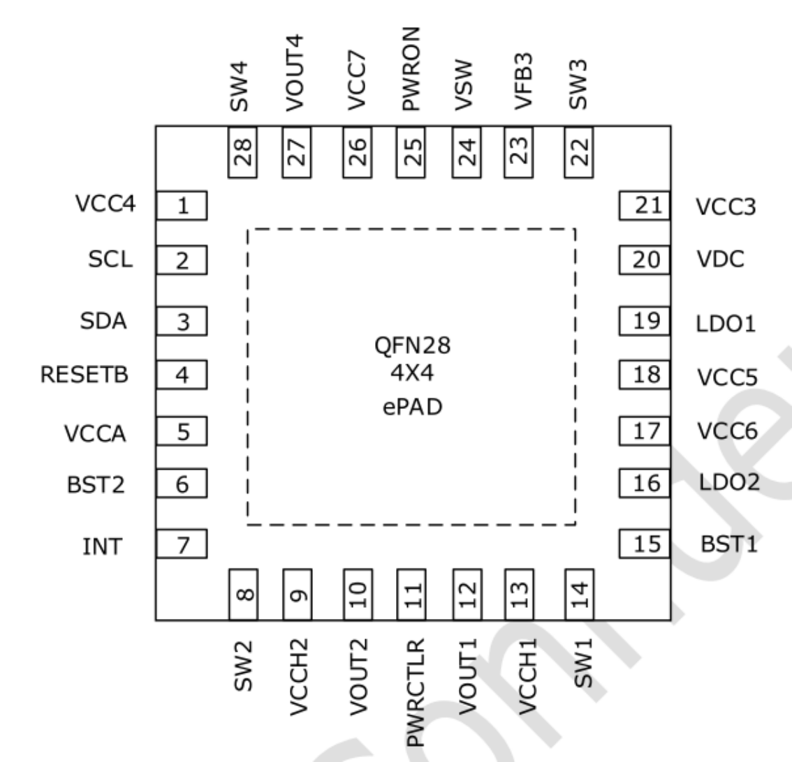
Original English figure — p.6
In the following description, PWRCTRL and INT pins need special attention:
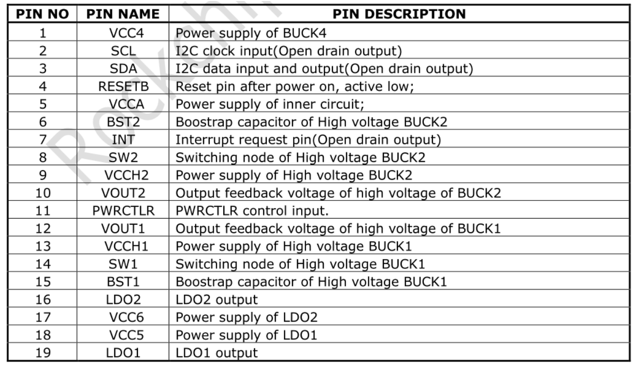
Original English figure — p.7
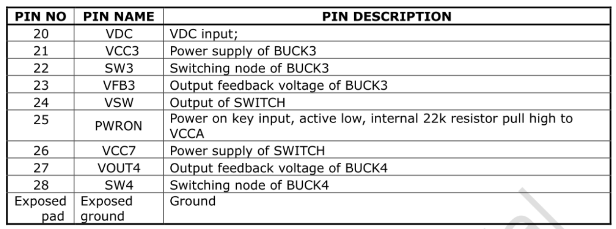
Original English figure — p.7
Pin definitions (transcribed row by row from the figures above; source names and I/O markers retained)
| Pin No. | Pin name | Description |
|---|---|---|
| 1 | VCC4 | Power supply of BUCK4 |
| 2 | SCL | I2C clock input (open drain output) |
| 3 | SDA | I2C data input and output (open drain output) |
| 4 | RESETB | Reset pin after power on, active low |
| 5 | VCCA | Power supply of inner circuit |
| 6 | BST2 | Bootstrap capacitor of high voltage BUCK2 |
| 7 | INT | Interrupt request pin (open drain output) |
| 8 | SW2 | Switching node of high voltage BUCK2 |
| 9 | VCCH2 | Power supply of high voltage BUCK2 |
| 10 | VOUT2 | Output feedback voltage of high voltage BUCK2 |
| 11 | PWRCTLR | PWRCTLR control input |
| 12 | VOUT1 | Output feedback voltage of high voltage BUCK1 |
| 13 | VCCH1 | Power supply of high voltage BUCK1 |
| 14 | SW1 | Switching node of high voltage BUCK1 |
| 15 | BST1 | Bootstrap capacitor of high voltage BUCK1 |
| 16 | LDO2 | LDO2 output |
| 17 | VCC6 | Power supply of LDO2 |
| 18 | VCC5 | Power supply of LDO1 |
| 19 | LDO1 | LDO1 output |
| 20 | VDC | VDC input |
| 21 | VCC3 | Power supply of BUCK3 |
| 22 | SW3 | Switching node of BUCK3 |
| 23 | VFB3 | Output feedback voltage of BUCK3 |
| 24 | VSW | SWITCH output |
| 25 | PWRON | Power on key input, active low, internal 22k resistor pull high to VCCA |
| 26 | VCC7 | Power supply of SWITCH |
| 27 | VOUT4 | Output feedback voltage of BUCK4 |
| 28 | SW4 | Switching node of BUCK4 |
| Exposed pad | Exposed ground | Ground |
1.4 Important Concepts
I2C Address 7-bit slave address: 0x27 PMIC has 3 working modes
- PMIC normal mode When the system is running normally, the PMIC is in normal mode, and at this time pmic_pwrctrl is at low level.
- PMIC sleep mode When the system enters sleep mode, the standby power consumption needs to be as low as possible. The PMIC will switch to sleep mode to reduce its own power consumption. At this time, it will generally reduce the output voltage of some paths or directly turn off the output, which can be configured according to actual product requirements. When the system is in standby, the
AP configures pmic_pwrctrl to sleep mode through I2C instructions, and then pulls up pmic_pwrctrl to let the PMIC enter sleep state; when the SoC wakes up, pmic_pwrctrl returns to low level, and the PMIC exits sleep mode.
- PMIC shutdown mode When the system enters the shutdown process, the PMIC needs to complete the power-down operation of the entire system. The AP configures pmic_pwrctrl to shutdown mode through I2C instructions, and then pulls up pmic_pwrctrl to let the PMIC enter shutdown state. Currently, the driver will automatically switch between the above modes according to DTS configuration and scenarios, so users do not need to be concerned about this. pmic_pwrctrl pin Normally at low level, the PMIC is in normal mode. When the pin is pulled high, it will switch to sleep or shutdown mode. pmic_int pin Normally at high level, it becomes low level when an interrupt occurs. If the interrupt is not handled, it will remain at low level. pmic_pwron pin The pwrkey function requires hardware to connect the power button to this pin, and the driver uses this pin to detect button press/release. Working modes of each DCDC DCDC has PWM (also called force PWM) and PFM modes, but PMIC has a mode that dynamically switches between PWM and PFM, which is what we usually call AUTO mode. PMIC supports PWM and AUTO PWM/PFM modes. AUTO mode has high efficiency but poor ripple transient response. For system stability considerations, it is set to PWM mode during runtime, and the system will switch to AUTO PWM/PFM when entering sleep. DCDC3 voltage adjustment DCDC3 power supply is special - the voltage cannot be modified through registers, it can only be adjusted through the voltage divider resistors in the external circuit. Therefore, if you need to modify the voltage, please modify the peripheral hardware. In Rockchip’s solution, it is generally used as VCC_DDR. Runtime voltage adjustment range of DCDC and LDO DCDC voltage range is discontinuous (see comments or datasheet):
// BUCK1
static const struct linear_range rk801_buck1_voltage_ranges[] = {
   REGULATOR_LINEAR_RANGE(500000,   0, 80, 12500), /* 0.5V - 1.5V, step 12.5mV */
   REGULATOR_LINEAR_RANGE(1800000, 81, 82, 400000),/* 1.8V - 2.2V */
   REGULATOR_LINEAR_RANGE(3300000, 83, 83, 0), /* 3.3V */
   REGULATOR_LINEAR_RANGE(5000000, 84, 84, 0), /* 5.0V */
   REGULATOR_LINEAR_RANGE(5250000, 85, 85, 0), /* 5.25V */
};

// BUCK2
static const struct linear_range rk801_buck2_voltage_ranges[] = {
   REGULATOR_LINEAR_RANGE(800000,  0, 2, 50000),   /* 0.8V - 0.9V */
   REGULATOR_LINEAR_RANGE(1800000, 3, 4, 400000),  /* 1.8V - 2.2V */
   REGULATOR_LINEAR_RANGE(3300000, 5, 5, 0),   /* 3.3V */
   REGULATOR_LINEAR_RANGE(5000000, 6, 6, 0),   /* 5.0V */
   REGULATOR_LINEAR_RANGE(5250000, 7, 7, 0),   /* 5.25V */
};

// BUCK4
static const struct linear_range rk801_buck4_voltage_ranges[] = {
   REGULATOR_LINEAR_RANGE(500000,   0, 80, 12500), /* 0.5V - 1.5V */
   REGULATOR_LINEAR_RANGE(1800000, 81, 82, 400000),/* 1.8V - 2.2V */
   REGULATOR_LINEAR_RANGE(2500000, 83, 83, 0), /* 2.5V */
   REGULATOR_LINEAR_RANGE(2800000, 84, 84, 0), /* 2.8V */
   REGULATOR_LINEAR_RANGE(3000000, 85, 85, 0), /* 3.0V */
   REGULATOR_LINEAR_RANGE(3300000, 86, 86, 0), /* 3.3V */
};
LDO voltage is continuous:
| Voltage range(V) | Step(mV) |
|---|---|
| 0.5 ~ 3.4 | 50 |
1.5 Power-on Conditions and Sequence
- Power-on Conditions PMIC can be powered on as long as any of the following conditions is met: VDC pin is high level Press PWRON key in power-off state to trigger
- Power-on Sequence Each SOC platform may have different requirements for the power-on sequence of each power supply. Currently, there are the following power-on sequences. For details, please refer to the latest datasheet.
2. Configuration
2.1 Driver and menuconfig
Driver files:
drivers/mfd/rk808.c
drivers/regulator/rk801-regulator.c
drivers/input/misc/rk805-pwrkey.c
menuconfig configuration:
CONFIG_MFD_RK808
CONFIG_REGULATOR_RK801
CONFIG_INPUT_RK805_PWRKEY
2.2 Driver Version
Please update to at least the following version to ensure the integrity and stability of driver functions. drivers/mfd/rk808.c:
commit 0439f30ead1393813d69a01587530652908c9171
Author: Joseph Chen <chenjh@rock-chips.com>
Date:   Fri Jun 13 17:19:25 2025 +0800

    mfd: rk808: Print full chip id of rk801

    Signed-off-by: Joseph Chen <chenjh@rock-chips.com>
    Change-Id: I195858d23c862d0f961acb4c04bb1102ab9954c9
drivers/regulator/rk801-regulator.c:
commit 1a81f4f6344f7cd4203be508150daeedc00fbedb
Author: Joseph Chen <chenjh@rock-chips.com>
Date:   Thu May 29 11:39:58 2025 +0800

    mfd: rk801: Add support for pwrctrl active pol set and reboot rst

    - Don't require pwrctrl dvs if hw compatible version >= 3.
    - Auto parse pwrctrl active pol from GPIO_ACTIVE_{HIGH,LOW} flag.
    - Reset pmic and soc when system reboot if required.

    Signed-off-by: Joseph Chen <chenjh@rock-chips.com>
    Change-Id: I29e60c2a717cee5c9d1e3c6e46ee687352d4a1be
2.3 DTS Configuration
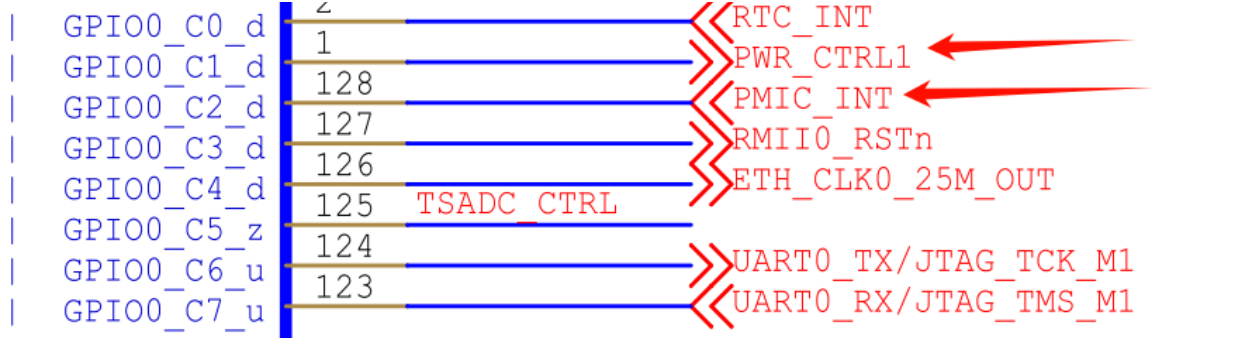
DTS configuration includes: I2C mounting, main body, regulator and other parts. The following takes arch/arm/boot/dts/rk3506-rk801.dts as an example. Hardware Design:
Original English figure — p.11
DTS Configuration:
&i2c0 {
    status = "okay";
    ......

    rk801: rk801@27 {
        // Cannot be modified.
        compatible = "rockchip,rk801";
        status = "okay";
        reg = <0x27>;

        // PMIC_INT pin configuration. Here is GPIO0_C2, active low.
        interrupt-parent = <&gpio0>;
        interrupts = <RK_PC2 IRQ_TYPE_LEVEL_LOW>;

        // PWRCTRL pin configuration. Here is GPIO0_C1, active high.
        pwrctrl-gpios = <&gpio0 RK_PC1 GPIO_ACTIVE_HIGH>;

        // Pinctrl configuration.
        pinctrl-names = "default", "pmic-reset";
        // Initialize pmic_int pin state.
        pinctrl-0 = <&pmic_int>;
        // Set the state of pwrctrl when rebooting. After this configuration, PMIC will reset its various voltages together with the SoC.
        pinctrl-1 = <&soc_pwrctrl_reset>;

        // Cannot be modified. Declare that RK801 has the function of managing system power-down.
        rockchip,system-power-controller;

        // Cannot be modified. Declare PMIC_INT as a wake-up source.
        wakeup-source;

        // Input sources for each regulator.
        // vcc1~7 correspond to: BUCK1/2/3/4, LDO1/2, SWITCH.
        vcc1-supply = <&vcc12v_dc>;
        vcc2-supply = <&vcc12v_dc>;
        vcc3-supply = <&vcc5v0_sys>;
        vcc4-supply = <&vcc5v0_sys>;
        vcc5-supply = <&vcc3v3_sys>;
        vcc6-supply = <&vcc3v3_sys>;
        vcc7-supply = <&vcc3v3_sys>;
        regulators {
            vcc3v3_sys: DCDC_REG1 {
                regulator-name = "vcc3v3_sys";
                regulator-min-microvolt = <3300000>;
                regulator-max-microvolt = <3300000>;
                regulator-initial-mode = <0x1>;
                regulator-boot-on;
                regulator-always-on;
                regulator-state-mem {
                    regulator-mode = <0x2>;
                    regulator-on-in-suspend;
                    regulator-suspend-microvolt = <3300000>;
                };
            };

            vcc5v0_sys: DCDC_REG2 {
                regulator-name = "vcc5v0_sys";
                regulator-min-microvolt = <5000000>;
                regulator-max-microvolt = <5000000>;
                regulator-initial-mode = <0x1>;
                regulator-boot-on;
                regulator-always-on;
                regulator-state-mem {
                    regulator-mode = <0x2>;
                    regulator-on-in-suspend;
                    regulator-suspend-microvolt = <5000000>;
                };
            };

            vcc_ddr: DCDC_REG3 {
                regulator-name = "vcc_ddr";
                regulator-boot-on;
                regulator-always-on;
                regulator-state-mem {
                    regulator-mode = <0x2>;
                    regulator-on-in-suspend;
                };
            };

            vdd_cpu: DCDC_REG4 {
                regulator-name = "vdd_cpu";
                regulator-min-microvolt = <500000>;
                regulator-max-microvolt = <1500000>;
                regulator-initial-mode = <0x1>;
                regulator-boot-on;
                regulator-always-on;
                regulator-state-mem {
                    regulator-mode = <0x2>;
                    regulator-off-in-suspend;
                };
            };
            vdd0v9_sys: LDO_REG1 {
                regulator-name = "vdd0v9_sys";
                regulator-min-microvolt = <900000>;
                regulator-max-microvolt = <900000>;
                regulator-boot-on;
                regulator-always-on;
                regulator-state-mem {
                    regulator-on-in-suspend;
                    regulator-suspend-microvolt = <900000>;
                };
            };

            vcc_1v8: LDO_REG2 {
                regulator-name = "vcc_1v8";
                regulator-min-microvolt = <1800000>;
                regulator-max-microvolt = <1800000>;
                regulator-boot-on;
                regulator-always-on;
                regulator-state-mem {
                    regulator-on-in-suspend;
                    regulator-suspend-microvolt = <1800000>;
                };
            };

            vcc_3v3: SWITCH_REG {
                regulator-name = "vcc_3v3";
                regulator-boot-on;
                regulator-always-on;
                regulator-state-mem {
                    regulator-on-in-suspend;
                };
            };
        };
    };
};

&pinctrl {
    ......

    pmic {
        // pmic_int is set to normally high level, that is, active low.
        pmic_int: pmic-int {
            rockchip,pins = <0 RK_PC2 RK_FUNC_GPIO &pcfg_pull_up>;
        };

        // The level state that the pwrctrl pin should maintain during system reset, must be opposite to the SoC's default power-on state.
        // For example: if the default power-on is down, configure as output high; otherwise, configure as output low.
        soc_pwrctrl_reset: soc-pwrctrl-reset {
            rockchip,pins = <0 RK_PC1 RK_FUNC_GPIO &pcfg_output_high>;
        };
    };
};
regulator configuration items: regulator-compatible : The name that needs to be matched when the driver is registered, cannot be changed, otherwise the loading will fail; regulator-name : The name of the power supply, it is recommended to keep it consistent with the hardware diagram, this name needs to be matched when using the regulator_get interface; regulator-init-microvolt : Initialization voltage in u-boot stage, invalid in kernel stage; regulator-min-microvolt : The minimum voltage that can be adjusted during runtime; regulator-max-microvolt : The maximum voltage that can be adjusted during runtime; regulator-initial-mode : DCDC working mode during runtime, generally configured as 1. 1: force pwm, 2: auto pwm/pfm; regulator-mode : DCDC working mode during sleep, generally configured as 2. 1: force pwm, 2: auto pwm/pfm; regulator-boot-on : When this attribute exists, this power supply will be enabled when registering the regulator; regulator-always-on : When this attribute exists, it means that this power supply is not allowed to be turned off during runtime and will be enabled when registering the regulator; regulator-on-in-suspend : Keep power-on state during sleep. To turn off this power supply, change it to “regulator-off-in-suspend”; regulator-suspend-microvolt : Standby voltage when power is not cut off during sleep. Description: If the voltages of regulator-min-microvolt and regulator-max-microvolt are equal, the system framework will set this voltage and enable this power supply by default when registering this regulator, without user intervention. If regulator-boot-on or regulator-always-on exists, the system framework will enable by default when registering this regulator. At this time, the voltage of this regulator has 2 situations: if the voltages of regulator-min-microvolt and regulator-max-microvolt are equal, the system framework will set this voltage to the current voltage value; if regulator-min-microvolt and regulator-max-microvolt differ, the PMIC hardware default power-on voltage is used.
pwrkey configuration items: If the pwrkey node is not specified under the rk801 node, it is equivalent to enabling. If you are sure to turn it off, please manually add the node and specify it as disabled .
rk801: rk801@27 {

    ......

    pwrkey {
        status = "disabled";
    };
};
2.4 Function Interfaces
The following interfaces can basically meet daily use, including regulator on, off, voltage setting, voltage getting, etc.:
- Get regulator: struct regulator *regulator_get(struct device *dev, const char *id) dev can be filled with NULL by default, id corresponds to the regulator-name attribute in dts.
- Release regulator void regulator_put(struct regulator *regulator)
- Enable regulator int regulator_enable(struct regulator *regulator)
- Disable regulator int regulator_disable(struct regulator *regulator)
- Get regulator voltage int regulator_get_voltage(struct regulator *regulator)
- Set regulator voltage int regulator_set_voltage(struct regulator *regulator, int min_uV, int max_uV) The passed-in parameters should ensure min_uV = max_uV, guaranteed by the caller.
- Example
struct regulator *rdev_logic;

rdev_logic = regulator_get(NULL, "vdd_logic");          // Get vdd_logic
regulator_enable(rdev_logic);                           // Enable vdd_logic
regulator_set_voltage(rdev_logic, 1100000, 1100000);    // Set voltage 1.1v
regulator_disable(rdev_logic);                          // Disable vdd_logic
regulator_put(rdev_logic);                              // Release vdd_logic
Description: Kernels 4.4 and higher also provide regulator interfaces starting with devm_ to help developers manage the resources they need to apply for.
3. Debugging
Because the drivers involved in PMIC are not complicated in terms of usage logic, the focus is on the final register settings. Users can use the kernel’s built-in i2cdump command, or they can use the following method: Node: /sys/rk8xx/rk8xx_dbg
# Read register
echo r [addr]  > /sys/rk8xx/rk8xx_dbg
# Write register
echo w [addr] [value] > /sys/rk8xx/rk8xx_dbg
Usage example:
echo r 0x2f > /sys/rk8xx/rk8xx_dbg          # Read the value of register 0x2f
echo w 0x2f 0x9c > /sys/rk8xx/rk8xx_dbg     # Set the value of register 0x2f to 0x9c
It is recommended to read it again after the write operation is completed to confirm whether the write was successful.
Editorial note: the pin table uses PWRCTLR, while the prose uses PWRCTRL. Source spellings are retained; verify hardware documentation before adaptation.