
Source V3.2.0: 44 Chinese pages and 46 English pages. Versions: RK3588 Linux 6.1/5.10, RT-Thread v5.1.x/v4.1.x; RK3568 Linux 6.1/5.10/4.19, RT-Thread v5.1.x/v4.1.x; RK1820 RT-Thread 5.1.x. RT-Thread is implemented only on the RK PCIe EP side. This is a platform reference: verify PCIe EP capability, pins, power, clocks, BSP and kernel for the actual ArmSoM board. Vendor EVB performance and compatibility results are not ArmSoM measurements. No hardware validation was performed. Chinese uses Chinese figures; the other languages use English originals.
Source issues retained for verification: R+2056B overlaps the preceding R+2560B in the small-memory BAR table; loopback refers to the speed_test README; Windows CTRL+L is listed as a suspend operation; Windows 10 2004, build 19042.1052 and eq configuration meanings require checking. Secure Boot/signature settings are historical development instructions, not operations performed here.
1. Overview of EP Card
The RK PCIe EP Standard Card Development Kit is a comprehensive development package of software and hardware for RK’s “PCIe EP Card” product form, based on the RK EP Card Demo Board (hereinafter referred to as the EP Card). The development kit primarily includes: Quick Operation Guide for EP Card EP Card Boot Scheme, PCIe-related hardware and software design development, and OTA upgrade content Basic Business of EP Card Business Examples under the Basic Framework of EP Card Business
2. EP Card Specifications
2.1 Basic Specifications
| Main Chip |
Boot Scheme | SMBus Expansion |
Independent Clock Scheme |
|---|---|---|---|
| RK3568 | Supports Flash Boot, Common Boot Does not support PCIe Boot |
N | Supports SRNS Does not support SRIS |
| RK3588 | Supports Flash Boot, Common Boot Does not support PCIe Boot |
N | N |
| RK1820 | Supports Flash Boot, Common Boot, EP Boot |
Y | N |
Explanation: Flash Boot includes: Flash Boot - Integrated PCIe Bin and EP Boot software scheme Flash Boot - Integrated PCIe Bin software scheme For EP boot schemes that do not support PCIe Boot, the PCIe protocol stipulates that the EP card should enter the detection mode within 20ms after the release of PERST#, followed by continuous detection, negotiation, and enumeration by the RC, which may take up to 100ms. Therefore, to enhance compatibility when the EP card interfaces with a general RC, it is recommended to choose SPI Flash as the boot storage to achieve quick startup, and SPI Nor is generally recommended as the boot storage.
2.2 Software Development
The EP card development package is essentially a PCIe product functionality demonstration development package, not a one-stop solution. Customers need to perform secondary development on PCIe and upper- layer applications based on this.
2.3 Operating Systems
EP Devices: EP cards are compatible with Linux, Android, and RT-Thread operating systems. RC Devices: EP cards compatible with Linux operating systems for RC devices have been verified on specific RCs. EP cards compatible with Windows operating systems for RC devices have been verified on specific RCs, but only basic transmission functions have been implemented. Other functions require customers to develop based on the Linux driver.
2.4 Clock Requirements
It is recommended that the EP card uses a homologous reference clock scheme, that is, the EP utilizes the 100M reference clock provided by the RC end. For EP cards that use RK chips for both RC and EP and support independent clock schemes, adopting an internal 100M clock for RC&EP can eliminate the need for an external clock generator and clock buffer chips.
2.5 PCI Device ID
The default ID for RK PCIe EP cards is the RK custom device ID. For third-party developers, the following requirements apply: Internal Use Devices: If the device is used only in a closed environment, you can use the existing VID of RK PCIe. External Devices: If the device is for sale or public use, you need to apply for a VID from PCI-SIG yourself.
2.6 Hot-Swapping
The RK PCIe Endpoint card does not support hot-swapping.
2.7 Auxiliary Signals
| Auxiliary Signal |
Function | Standard EP Solution | RK Chip Interconnect Independent Power Supply Solution |
|---|---|---|---|
| PRSNT# | N | ||
| PERST# | GPIO Input | Mandatory, connected to system reset, full board reset |
Mandatory, GPIO input, software reset, configure dts reset-gpios; |
| CLKREQ# | FUNCTION Input |
Optional, used to extend ASPM L1SS power management, not implemented yet but recommended to reserve, if no clear demand can be left unconnected |
Optional, used to extend ASPM L1SS power management, not implemented yet but recommended to reserve, if no clear demand can be left unconnected |
| JTAG | N | ||
| SMBus | N | ||
| WAKE# | GPIO Output |
Mandatory, extend sleep wake-up function, not implemented yet but recommended to reserve |
Mandatory, extend sleep wake-up function, configure dts wake- gpios; |
| +3.3Vaux | N |
Explanation: The RK chip interconnect independent power supply scheme involves scenarios where one end drops power, it is recommended to do IO protection to prevent the risk of voltage/current injection when one end drops power and the other end IO continues to output. Pins with GPIO function should not be configured as PCIe function in pinctrl, support any pin, no restrictions. Auxiliary signals with FUNCTION should select the corresponding functional pins. Standard EP scheme PERST# connects to system reset for full board reset requirements: The PERST# signal serves as the last resort for physical reset of EP on the RC side. There are special RC compatibility issues, for example: RC enumeration completes and immediately enters L2 through PERST# reset, requiring a quick reset. NOTE: Since the RC’s PERST is PP strong drive, and the EP’s PMIC is an OD pin, regardless of whether the RC’s PERST is 3.3V or 1.8V, it is necessary to drive the EP side’s RESET_L through circuit conversion.
2.8 Performance Specifications
Users should clearly understand the PCIe transfer bandwidth requirements, data flow direction (RC/EP unidirectional? Bidirectional?), and whether there are fragmented control flows/large block data flows. It is recommended to: Read the “Measured Performance” section to understand the upper limit performance of the chips_connect development package: Read the “Performance | User Space Test Demo - pcie_speed_test” section to understand the transfer bandwidth for different block sizes.
3. EP Card Operation Guide
3.1 Environment Preparation
The EP card supports connection with general RC and RK RC, and this section provides a brief explanation of the basic functional verification for both scenarios.
3.1.1 Hardware Environment
RK3588 EP Board (Standard Card) Interface with RK3588 RC Reference Hardware Environment RC: RK3588-EVB1-V10 Connect the power cable, serial cable, USB-to-Type-C firmware download cable, HDMI output cable (connected to HDMI_OUT0) EP: RK3588-EVB4-V11 RC provides direct power supply, no separate power cable needed, hot-plugging is not supported, connect before powering on the RC. RK3588 EP Board (Standard Card) Interface with General RC RC: PC EP: RK3588-EVB4-V11 RC provides direct power supply, no separate power cable needed, hot-plugging is not supported, connect before powering on the RC. RK3588 Chip Interconnection Independent Power Supply Scheme Reference Hardware Environment RC: RK3588-EVB1-V10 Connect the power cable, serial cable, USB-to-Type-C firmware download cable, HDMI output cable (connected to HDMI_OUT0) EP: RK3588-EVB4-V12 EP board is independently powered, R8114 and R2005 are not populated
It is required to connect PERST#, WAKE# signals, and use them as GPIOs Connect the power cable, serial cable, USB-to-Type-C firmware download cable
3.1.2 Software Environment
The loader, uboot, boot, and file system required by the chip can be obtained from the images directory of the release package, where these image files are located. Flash Boot - Integrated PCIe Bin Software Solution Taking the RK3588 EP board as an example, the boot files are shown in the table below:
| Item | File Name | Description |
|---|---|---|
| RC (Not required for general RC interface) | rk3588-update-rc-evb7-v11.img | Flashed to RC Flash |
| EP | rk3588-update-ep-evb4-v11.img | Flashed to EP Flash |
Note: The update.img file includes MiniLoaderAll.bin, uboot.img, boot.img, rootfs.img, and other files. Flash Boot - Integrated PCIe Bin and EP Boot Software Solution Taking the RK3588 EP board as an example, the boot files are shown in the table below:
| Item | File Name | Description |
|---|---|---|
| RC (Not required for general RC interface) |
rk3588-update-rc-evb7-v11.img | Flashed to RC Flash |
| EP | RK3588_MiniLoaderAll.bin | Flashed to EP Flash |
| EP | pcie_idb.img | Flashed to EP Flash |
| EP | normal_idb.img | Flashed to EP Flash |
| EP | uboot.img | Imported into EP DDR memory by RC via PCIE |
| EP | boot.img (including kernel+rootfs) |
Imported into EP DDR memory by RC via PCIE |
Note: For RC to download firmware to EP via PCIE, please refer to the next section on functional verification instructions.
3.2 Functional Verification
The sample code for verifying the functionality of PCIe EP is located in the examples directory of the SDK release package, including the sample codes used by EP and RC, encapsulated message communication code, and encapsulated data communication code.
3.2.1 Linux RC
The necessary bins and resources for general RC functionality verification are stored in the images directory and need to be manually copied to the RC platform (only for X86 platforms). RK RC resources are directly packaged into the firmware root directory without additional operations. After preparing the hardware and software environment, the steps to perform a complete PCIE functionality verification are as follows. If you do not need to download firmware to the EP card, you can skip the first point directly.
- RC downloads firmware to EP via PCIE Step 1. The EP card’s serial port baud rate is 1500000 (the RC baud rate is also 1500000). After connecting the serial port, it will continuously print the following log, indicating that the PCIE link between EP and RC is successful and waiting for RC to transmit firmware.
U-Boot SPL 2017.09-g614fe864bf-dirty #xyp (Apr 20 2023 - 11:19:22)
RKEP: 191277 - Link ready! Waiting RC to download Firmware:
RKEP: 191723 - Download uboot.img  to BAR2+0
RKEP: 192068 - Download boot.img   to BAR2+0x400000
RKEP: 192466 - Send CMD_LOADER_RUN to BAR0+0x400
RKEP: 1092850 - Waiting for FW, CMD: 0
RKEP: 2093146 - Waiting for FW, CMD: 0
RKEP: 3093443 - Waiting for FW, CMD: 0
RKEP: 4093740 - Waiting for FW, CMD: 0
RKEP: 5094036 - Waiting for FW, CMD: 0
Note: If the EP card directly enters the system, it means that the flash contains a complete firmware. Please rewrite pcie_idb.img and normal_idb.img under maskrom. Step 2. Execute ./pcie_download_test_rc 0 ./uboot.img ./boot.img on the RC side to initiate data transfer between RC and EP. The firmware is moved to the specified memory address of the EP card via DMA, and then a startup instruction is sent to let EP boot via DDR. At this point, the EP card will print the normal boot log and enter the system. Note: If an exception occurs when executing the application on the RC side, please refer to examples/pcie_download_test/README to troubleshoot the issue.
- Video Decoding Preview Sample Step 1. The EP card’s serial port baud rate is 1500000 (the RC baud rate is also 1500000). After connecting the serial port, executing lspci -vvv |grep 356a and ls /dev/pcie-rkep* on the RC side will show the following devices, indicating that the EP card is recognized and the RC driver is loaded normally.
[root@RK3588:/userdata]# lspci -vvv |grep 356a
01:00.0 Processing accelerators: Rockchip Electronics Co., Ltd Device 356a (rev 01)
[root@RK3588:/userdata]# ls /dev/pcie-rkep*
/dev/pcie-rkep0000:01:00.0
Step 2. After the EP card enters the system normally, the terminal will print the following log and be blocked, waiting for the RC application to start.
00:00:05.330 I [cmp_pcie_ep: cc_cmp_pcie_device: 390] rk pcie version: v3.0.0 - 2024-12-11
00:00:05.330 D [chipscon: cc_kernel_api_prob: 398] open rkep: /dev/pcie_ep Success.
00:00:05.330 D [chipscon: cc_kernel_api_prob: 403] probe pcie_rkep, fd = 3
00:00:05.330 I [core_pcie_ep: cc_core_pcie_dev_i: 53] bar0 size=0x400000
00:00:05.330 I [core_pcie_ep: cc_core_pcie_dev_i: 53] bar2 size=0x4000000
00:00:05.330 I [core_pcie_ep: cc_core_pcie_dev_i: 53] bar4 size=0x100000
00:00:05.330 E [chipscon: cc_kernel_api_reso: 141] cc_kernel_api_resource_mmap mmap failed, size=0, err=Invalid argument
00:00:05.330 E [core_pcie_ep: cc_core_pcie_dev_i: 73] no bar1
00:00:05.330 E [chipscon: cc_kernel_api_reso: 141] cc_kernel_api_resource_mmap mmap failed, size=0, err=Invalid argument
00:00:05.330 E [core_pcie_ep: cc_core_pcie_dev_i: 86] no bar5
00:00:05.330 I [pcie_dma: cc_core_pcie_dma_i: 590]  - id=ffffffff
00:00:05.330 I [pcie_dma: cc_core_pcie_dma_i: 600]  - id=356a1d87
00:00:05.330 I [pcie_dma: cc_core_pcie_dma_i: 609]  - magic=524b4550, ver=1
......
00:00:05.331 D [cmp_pcie_ep: pcie_task_ep_msg_t: 264]  start
00:00:05.331 D [cmp_pcie_ep: stream_speed_threa: 352] stream_speed_thread tart
Step 3. Refer to the User Layer Memory Configuration Section to configure the memory for the RC system. Step 4. Execute the following instructions on the RC to complete the handshake with the EP card and initiate data transfer between them. General RC: ./pcie_video_test_rc ./output1.h264 36 704 576 0 1 RK RC: pcie_video_test_rc /root/output1.h264 36 704 576 0 1 At this point, the RC’s display device will output a resolution of 1080P60, and you can see 36 video decoding streams and the first NN human detection feature. Note: The RC side outputs display data through the DRM display framework. The RK RC supports it by default; general RC requires installing the libdrm-dev component and switching to another terminal without GUI by pressing ctr+F3 before executing the test command. Step 4. If you need to stop the Sample program, you can press the Enter key in the RC application, which will send a message to the EP card to destroy the relevant business and exit the program; the EP card will destroy the relevant business and exit the program after receiving the message. A normal business exit process is required; otherwise, the EP card business will not exit, leading to abnormal operation in the next run. Note:
The EP side application defaults to self-start and loop start upon boot. If you need to run other test programs, you need to comment out the current test in the boot script and then restart the RC and EP. Modify /etc/init.d/S99_pcie_ep.sh and comment out the following code.
while true;
do
    cd /
    pcie_video_test_ep 1
done &
3.2.2 Windows RC
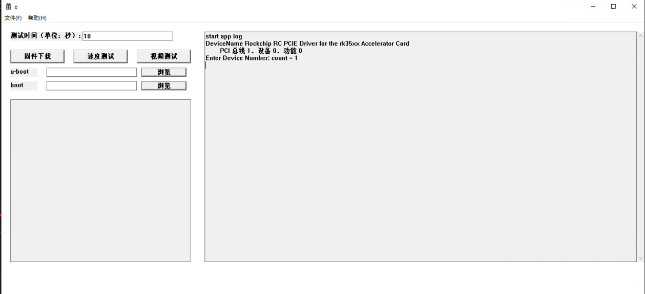
Windows RC provides drivers that only support systems below Windows 10 version 2004. Higher version systems require building a driver compilation environment to compile the drivers on their own. Refer to the Building Windows Driver Environment section to set up the test environment, focusing only on system version and disabling driver signature enforcement steps. After confirming the system environment, insert the EP card and power on the PC. You can see the PCI device in Device Manager, right-click on the device and select “Update Driver” -> “Browse my computer for driver software” -> set to the provided driver directory (Win-Driver-RC) -> Next to install the driver. After installation, you can see the Rockchip RC PCIE Driver for the rk35xx Accelerator Card device in Device Manager. Run the test tool with administrator privileges. The tool is shown in the figure below, currently supporting firmware download, rate testing, and video decoding object detection testing. If the tool reports an error, refer to the Common Problem Handling Section.
Original technical figure, page 13
After preparing the hardware and software environment, the steps to perform a complete PCIE function verification are as follows. If you do not need to download firmware to the EP card, you can skip the first point directly.
- RC downloads firmware to EP via PCIE
Step 1. The serial port baud rate of the EP card is 1500000 (the RC baud rate is also 1500000). After connecting the serial port, it will continuously print the following log, indicating that the PCIE link between EP and RC is successful and waiting for RC to transmit firmware.
U-Boot SPL 2017.09-g614fe864bf-dirty #xyp (Apr 20 2023 - 11:19:22)
RKEP: 191277 - Link ready! Waiting RC to download Firmware:
RKEP: 191723 - Download uboot.img  to BAR2+0
RKEP: 192068 - Download boot.img   to BAR2+0x400000
RKEP: 192466 - Send CMD_LOADER_RUN to BAR0+0x400
RKEP: 1092850 - Waiting for FW, CMD: 0
RKEP: 2093146 - Waiting for FW, CMD: 0
RKEP: 3093443 - Waiting for FW, CMD: 0
RKEP: 4093740 - Waiting for FW, CMD: 0
RKEP: 5094036 - Waiting for FW, CMD: 0
Note: If the EP card directly enters the system, it means that the flash contains a complete firmware. Please rewrite pcie_idb.img and normal_idb.img in the maskrom. Step 2. Open the tool to load uboot and boot firmware, then click on firmware download. The tool will transfer the firmware to the specified memory address of the EP card via DMA and then send a start instruction to let EP boot via DDR. At this point, the EP card will print the normal boot log and enter the system.
- Video Decoding Preview Test Step 1: After the EP card enters the system normally, the terminal will print the following log and be blocked, waiting for the RC application to start.
00:00:05.330 I [cmp_pcie_ep: cc_cmp_pcie_device: 390] rk pcie version: v3.0.0 - 2024-12-11
00:00:05.330 D [chipscon: cc_kernel_api_prob: 398] open rkep: /dev/pcie_ep Success.
00:00:05.330 D [chipscon: cc_kernel_api_prob: 403] probe pcie_rkep, fd = 3
00:00:05.330 I [core_pcie_ep: cc_core_pcie_dev_i: 53] bar0 size=0x400000
00:00:05.330 I [core_pcie_ep: cc_core_pcie_dev_i: 53] bar2 size=0x4000000
00:00:05.330 I [core_pcie_ep: cc_core_pcie_dev_i: 53] bar4 size=0x100000
00:00:05.330 E [chipscon: cc_kernel_api_reso: 141] cc_kernel_api_resource_mmap mmap failed, size=0, err=Invalid argument
00:00:05.330 E [core_pcie_ep: cc_core_pcie_dev_i: 73] no bar1
00:00:05.330 E [chipscon: cc_kernel_api_reso: 141] cc_kernel_api_resource_mmap mmap failed, size=0, err=Invalid argument
00:00:05.330 E [core_pcie_ep: cc_core_pcie_dev_i: 86] no bar5
00:00:05.330 I [pcie_dma: cc_core_pcie_dma_i: 590]  - id=ffffffff
00:00:05.330 I [pcie_dma: cc_core_pcie_dma_i: 600]  - id=356a1d87
00:00:05.330 I [pcie_dma: cc_core_pcie_dma_i: 609]  - magic=524b4550, ver=1
......
00:00:05.331 D [cmp_pcie_ep: pcie_task_ep_msg_t: 264]  start
00:00:05.331 D [cmp_pcie_ep: stream_speed_threa: 352] stream_speed_thread tart
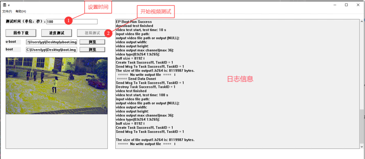
Step 2: Copy the test clip to the tool directory and rename it to output1.h264 . The current tool fixes the test clip as h264 raw stream. Set the test time, then click the video test button to run the test. Test screen as follows:
Original technical figure, page 15
3.3 Measured Performance
PCIE EP Transfer Performance
| EP | RC | Hardware Configuration |
Scenario | Maximum Transfer Rate |
|---|---|---|---|---|
| RK3588 | RK3588 | PCIE 3.0x4 Lane | EP Writes Data to RC | 2.95GB/s |
| EP Reads Data from RC | 1.8GB/s | |||
| EP Simultaneous Read/Write with RC |
Each 1.6GB/s | |||
| RK3588 | RK3588 (Enable Using RC DMA) |
PCIE 3.0x4 Lane | EP Writes Data to RC | 2.95GB/s |
| EP Reads Data from RC | 2.95GB/s | |||
| EP Simultaneous Read/Write with RC |
Each 2.85GB/s | |||
| X86 | PCIE 3.0x4 Lane | EP Writes Data to RC | 2.9GB/s | |
| EP Reads Data from RC | 2.5GB/s | |||
| EP Simultaneous Read/Write with RC |
Each 2.4GB/s | |||
| Windows | PCIE 3.0x4 Lane | EP Writes Data to RC | 650MB/s | |
| EP Reads Data from RC | 700MB/s | |||
| EP Simultaneous Read/Write with RC |
Each 320MB/s |
Performance will continue to be optimized. Windows does not currently support chain DMA testing, and the transfer rate is significantly affected by the memory structure; higher rates are achieved with large blocks of contiguous memory.
3.4 Compilation of Samples
For compilation and usage instructions of each sample, please refer to examples/*/README .
4. EP Card Business Basics
4.1 Principle Introduction
The EP card business primarily involves transferring source data and target data processed by the processor through the PCIe link between upstream and downstream. The main resources include: RC Side Manipulate PCIe EP devices through the open-source standard library libpci. Complete with the pcie-rkep driver: BAR mapping, recommended as a control flow transfer method DMA transfer, recommended as a data block transfer method Handle MSI interrupts, with the user layer actively polling to wait for an increase in response rate, but involving multiple handshakes, real-time performance is average Trigger ELBI interrupts Apply for DMA memory Support for multi-process, such as supporting the operation of multiple pcie_speed_test routines EP Side Complete with the pcie_ep driver: Default class id 0x1200 (Processing accelerators) BAR inbound physical address space mapping DMA transfer Send MSI interrupts Handle ELBI interrupts, with the user layer actively polling to wait for an increase in response rate, but involving multiple handshakes, real-time performance is average Support for multi-threading Hardware resources such as VDEC, VENC, RGA, GPU, NPU can be called at the user layer through Rockit or RKNN.
5. Introduction to Chips Connect
5.1 Principle Introduction
Chips Connect development kit is a user-level development kit built based on the EP card business foundation, primarily providing interface references for commonly used functions such as RC, EP uplink and downlink data transmission, and message notifications, while also constructing typical business scenarios for reference. BAR Space Allocation (common platforms) For general schemes with sufficient memory allocation, BAR space allocation during SPL and Kernel stages:
| BAR Space | Start Address |
End Address |
Function |
|---|---|---|---|
| BAR0 | 0 | 4KB | EP reserved space, driver version information, interrupt status, etc. |
| 12KB | 16KB | DEBUG function-related configuration information. |
|
| 16KB | 128KB | EP device status information. | |
| 128KB | 1M | User-defined. | |
| 1M | 4M | Framework command interaction and buff management. |
|
| BAR1 (Defaut Disabled) |
0 | 1MB | User-defined, how to enable refer to the “BAR Size Configuration” section. |
| BAR2 (BAR2/3 Bar Repair) |
0 | 64MB | Using RC DMA. |
| BAR4 | 0 | 4MB | Wired register area, used for operating DMA. |
| BAR5 (Defaut Disabled) |
0 | 1MB | User-defined, how to enable refer to the “BAR Size Configuration” section. |
Explanation: EP end BAR user-defined space can be used for secondary development expansion, the rest of the BAR space is the space required for the business code, for example: BAR1 is disabled by default, all space is user-defined, and when enabled, it is used for control flow. BAR5 is disabled by default, all space is user-defined, and when enabled, it is used for control flow. The EP end BAR inbound CPU address is fixed by the “BAR Mapping Configuration” by default and supports dynamic adjustment on the RC end.
BAR Space Allocation (memory-constrained platforms) For special schemes with tight memory allocation, BAR space allocation during SPL and Kernel stages:
| BAR Space | Start Address |
End Address |
Function |
|---|---|---|---|
| BAR0 | 0 | Reserved | Reserved space, default is 0. |
| R | R+2048B | EP reserved space, driver version information, interrupt status, etc. |
|
| R+2048B | R+2560B | DEBUG function-related configuration information. |
|
| R+2056B | R+3072B | EP device status information. | |
| R+3072B | R+4KB | User-defined. | |
| R+4KB | R+64KB | Framework command interaction and buff management. |
|
| BAR1 (Defaut Disabled) |
1MB | User-defined, how to enable refer to the “BAR Size Configuration” section. |
|
| BAR2 (BAR2/3 Bar Repair) |
0 | 64MB | Using RC DMA. |
| BAR4 | 0 | 4MB | Wired register area, used for operating DMA. |
| BAR5 (Defaut Disabled) |
0 | 1MB | User-defined, how to enable refer to the “BAR Size Configuration” section. |
Explanation: Reserved space: The minimum alignment of BAR is 1MB, and it is usually required to apply for 1MB of memory for mapping. However, in environments with tight memory, reserved processing is allowed, and the chips connect business uses the reserved memory. EP end BAR user-defined space can be used for secondary development expansion, the rest of the BAR space is the space required for the business code, for example: BAR1 is disabled by default, all space is user-defined, and when enabled, it is used for control flow. BAR5 is disabled by default, all space is user-defined, and when enabled, it is used for control flow. The EP end BAR inbound CPU address is fixed by the “BAR Mapping Configuration” by default and supports dynamic adjustment on the RC end.
5.2 PCIe Transfer System Architecture
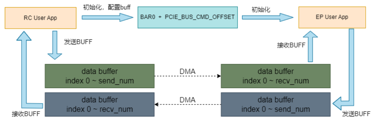
PCIE RC and EP System Block Diagram
Original technical figure, page 19
5.3 BUFF Management Structure and Data Transfer
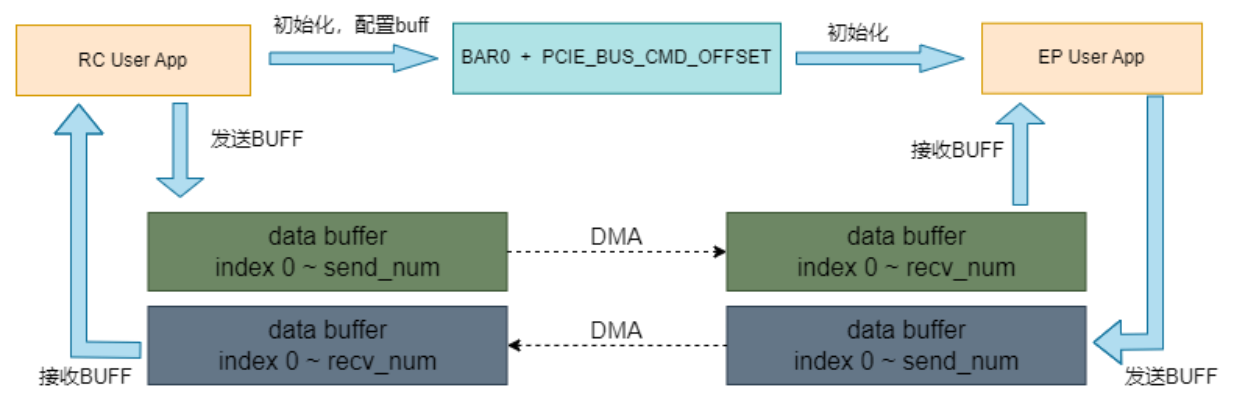
BUFF Management
Original technical figure, page 19
Here is a brief explanation from the RC perspective on the initialization to a complete read-write process:
5.3.1 Initialization Phase
Primarily, two tasks are performed:
-
Initialize the corresponding PCIe device based on VENDOR_ID, DEVICE_ID, and bus address. Internally, this is mainly achieved by iterating through the system’s PCIe devices via the libpci interface and mapping the BAR space to the application layer. It supports calling the rk_pcie_device_init interface repeatedly with different device IDs to initialize the device.
-
Call rk_pcie_task_create to create a task for initializing memory and BUFF status. The number and size of BUFFs can be set through the struct pcie_task_attr_st structure. The configuration information is passed to the EP device through the BAR0 space and waits for the EP device to complete
initialization. The EP retrieves the task creation message through rk_pcie_get_task_msg and then calls task initialization, facilitating an initialization configuration interaction between both sides. The RC-side application, based on compilation configuration information, selects Hugepage/RKEP/RKDRM methods to allocate memory. Each EP card device will generate a corresponding /dev/pcie-rkep* node on the RC side and allocate separate contiguous large memory (requires corresponding configuration to be enabled). After receiving the configuration information, the EP initializes the BUFF status and calls the interface to apply for physically contiguous memory, supporting Hugepage/RKDRM methods for memory allocation. The BUFF information for both RC and EP is ultimately assigned to a specific area of BAR0, which is used for BUFF status management.
#define VENDOR_ID                   0x1d87
#define DEVICE_ID                   0x356a

struct pcie_dev_bus dev_bus;
int ret;
//获取系统匹配的PCI设备总线地址
ret = rk_pcie_get_pci_bus_addresses(VENDOR_ID, DEVICE_ID, &rc_ctx.dev_bus);
if (ret != 0) {
    printf("get pci bus address fail\n");
    return -1;
}

printf("ep dev max num : %d\n", rc_ctx.dev_bus.dev_max_num);
if (rc_ctx.dev_bus.dev_max_num == 0) {
    printf("no ep device, exit ... \n");
} else {
    rc_ctx.dev_attr.using_rc_dma = 0;
    rc_ctx.dev_attr.rc_dma_chn = 0;
    rc_ctx.dev_attr.enable_speed = 1;
    rc_ctx.dev_attr.vendor_id = VENDOR_ID;
    rc_ctx.dev_attr.device_id = DEVICE_ID;
    rc_ctx.dev_attr.use_dma_only_in_rc = 0;
    rc_ctx.dev_attr.mem_type = E_MEM_TYPE_HUGEPAGE;
    memcpy(rc_ctx.dev_attr.pci_bus_address, pci_bus_address, strlen(pci_bus_address));

    //选择第⼀个匹配设备初始化
    rc_ctx.rk_handle = rk_pcie_device_init(&rc_ctx.dev_attr);
    //获取EP设备模式
    rk_pcie_get_ep_mode(rc_ctx.rk_handle, &rc_ctx.devmode);
    printf("ep device init, dev mode: %d, submode: %d\n", rc_ctx.devmode.mode,
rc_ctx.devmode.submode);
}
5.3.2 Sending Data
Sending data can be divided into three steps:
-
Check if there is an available BUFFER.
-
Obtain the available BUFFER and write data into it.
-
Send the BUFFER to the other end. Taking the sending of a BUFFER as an example, initializing the configuration send_buff_num = 5 indicates that there can be at most 5 sending BUFFERs in the system. The sender calls the interface to obtain an available BUFFER, and can then access the physical address and virtual address of the BUFFER, as well as the size of the BUFFER, through the properties of struct pcie_buff_node . After that, business operations can be performed. Finally, the sending interface is called to transmit the BUFFER data to the other end. Inside the sending interface, it will first flush the cache of the BUFFER to ensure that the physical memory contains the most recent data, and then call the DMA interface to transfer the data to the other end. The size of the data transferred by DMA is node->size , which should not exceed the size of the BUFFER. Note: The BUFFER sent to the other end needs to be released by the other end before it can become available again. If the other end does not release it, the entire process will be blocked. rk_pcie_get_buff does not support blocking mode temporarily, so it is necessary to call sleep to wait in a loop.
struct pcie_buff_node *node = rk_pcie_get_buff(rk_handle, E_SEND);
if(node) {
    node->size = rk_pcie_get_buff_max_size(rk_handle, E_SEND);
    //操作buff 写⼊数据
    rk_pcie_send_buff(ctx->rk_handle, node);
} else {
    usleep(1000);
}
RC Sending Data to EP Principle:
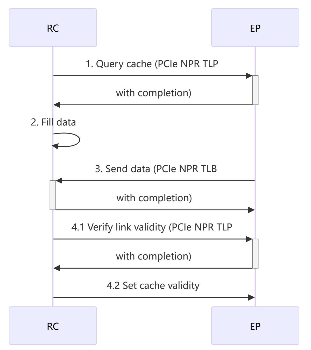
Original technical figure, page 22
EP Sending Data to RC Principle:
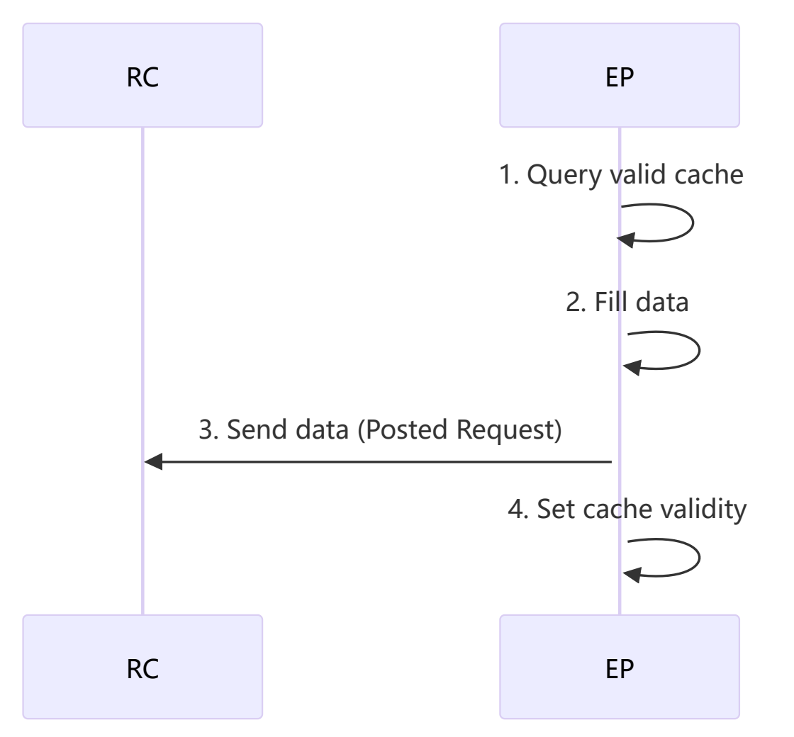
Original technical figure, page 23
5.3.3 Receiving Data
Receiving data can be divided into three steps:
-
Check if there is an available BUFFER.
-
Acquire the available BUFFER and read the data.
-
Release the BUFFER. Receiving BUFFER and sending BUFFER have similar internal implementations. The number of BUFFERs in the system is configured based on the initialization of recv_buff_num . Specific behavior can be referenced in the section on sending data. The size of the available data in the BUFFER is node->size .
struct pcie_buff_node *node = rk_pcie_get_buff(rk_handle, E_RECV);
if(node) {
    //操作buff 读取数据
    rk_pcie_release_buff(rk_handle, node);
} else {
    usleep(1000);
}
EP Data Reception Principle:
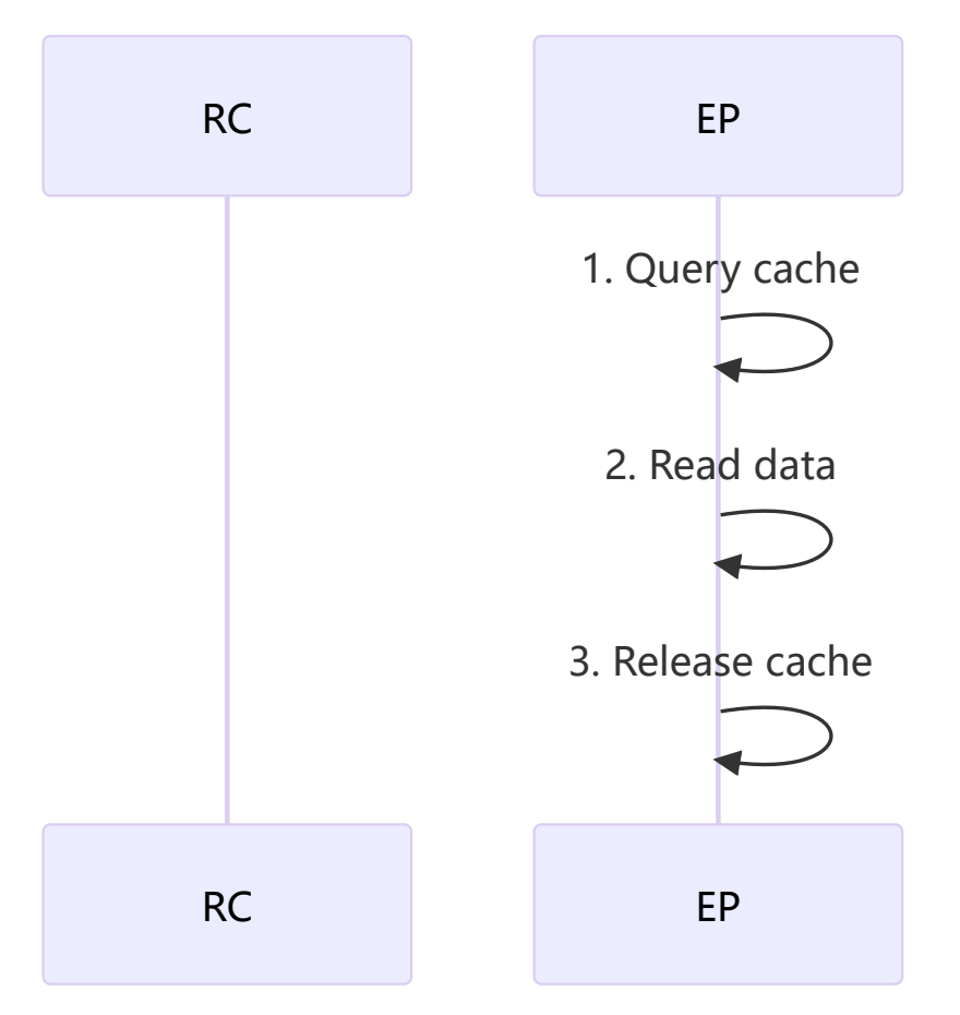
Original technical figure, page 24
RC Data Reception Principle:
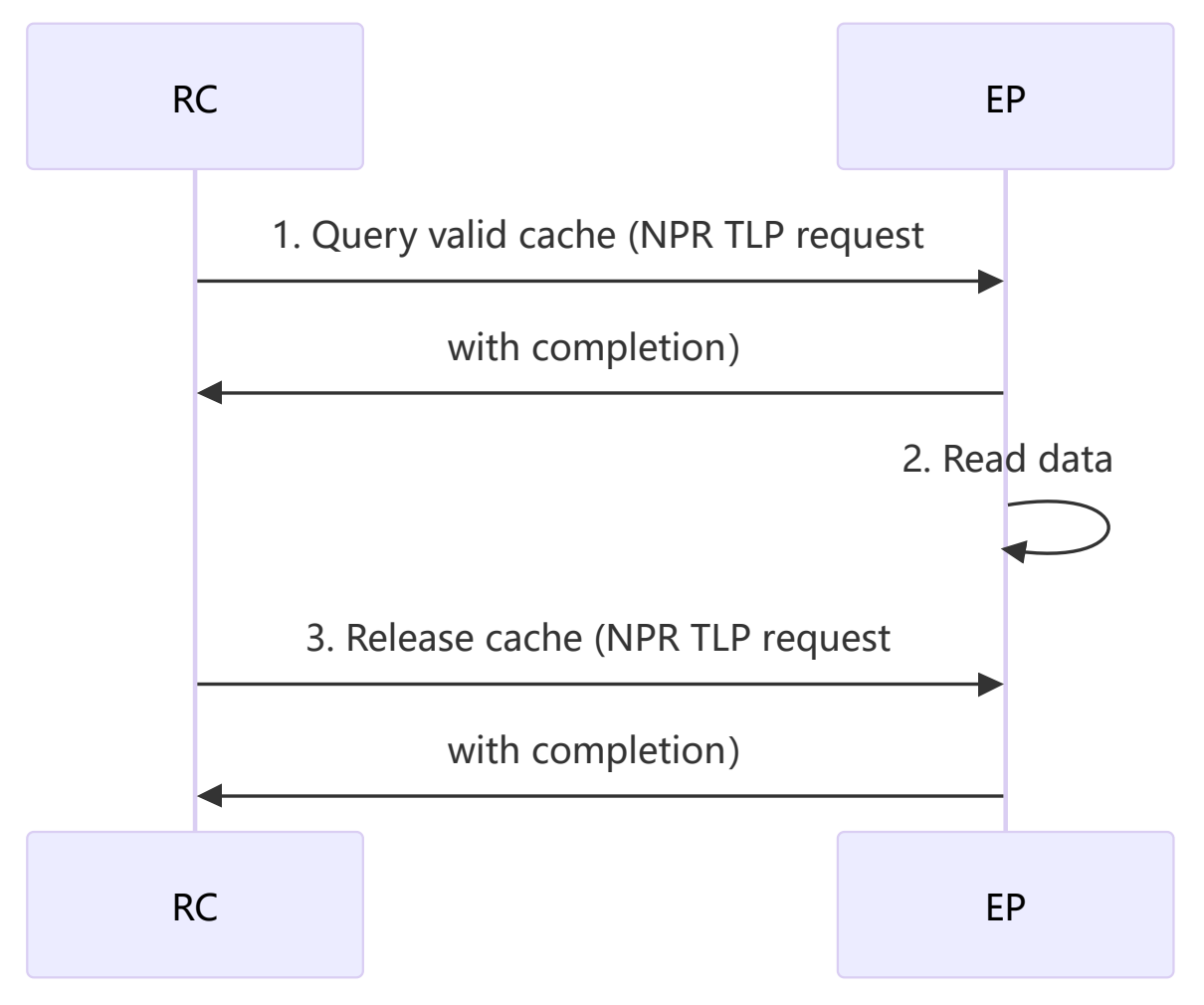
Original technical figure, page 24
5.3.4 BUFF Configuration
-
BUFF Configuration for RC to EP Transmission In the decoding card scenario, the RC end sends raw streams to the EP, with relatively low data volume per channel. A BUFF size of 4KB*video channel can be allocated. Each video stream transmits a size of 4KB per transfer, ensuring that each transmission can update the data and that the data volume is not too small to waste the PCIe bandwidth. It is recommended to configure 3-5 BUFFs for rotation use. At least three BUFFs must be configured; if additional processing is required for the BUFF, the number of BUFFs should be increased, otherwise, it will cause rotation to stall and affect the transmission rate. Multi-threaded transmission can appropriately increase the number of BUFFs.
-
BUFF Configuration for EP to RC Transmission. The data sent from EP to RC is usually decoded data, which is generally larger, such as a single frame of 1080p decoded into YUV422 data being approximately 3MB in size. A single BUFF can be configured to be 3MB-6MB in size, transmitting 1 or 2 channels of decoded data per transfer. Since multiple BUFFs are needed for rotation, a single BUFF should not be configured too large to avoid occupying too much memory space.
5.4 User-Level Memory Configuration
Both RC and EP support various memory allocation methods: RC side:
-
Memory allocation via the pcie-rkep driver, SDK obtains it through mmap mapping. Enable configuration: CONFIG_PCIE_FUNC_RKEP_USERPAGES=y (disabled by default) Modify memory size: Modify the macro RKEP_USER_MEM_SIZE in the driver pcie-rkep.c (default is 64M)
-
Memory allocation through HugePages. (Recommended method)
-
Memory allocation via the DRM driver, requiring pre-allocation of CMA in the dts. Modify DMA memory size in device tree: arch/arm64/boot/dts/rockchip/rk3588-linux.dtsi
@@ -71,7 +71,7 @@ reserved-memory {
cma {
    compatible = "shared-dma-pool";
    reusable;
    reg = <0x0 0x50000000 0x0 0x10000000>; //从地址0x50000000开始256MB⼤⼩
    linux,cma-default;
};
-
Dummy method, where the data buffer is managed by the user, and the framework only manages the rotation node without allocating the data buffer. Currently, only supports Windows systems. EP side:
-
Memory allocation via the DRM driver, requiring pre-allocation of CMA in the dts. Modify DMA memory size in device tree: arch/arm64/boot/dts/rockchip/rk3588-linux.dtsi
@@ -71,7 +71,7 @@ reserved-memory {
cma {
    compatible = "shared-dma-pool";
    reusable;
    reg = <0x0 0x50000000 0x0 0x10000000>; //从地址0x50000000开始256MB⼤⼩
    linux,cma-default;
};
- Memory allocation through HugePages. (Recommended method) Different memory allocation methods can be specified through attributes during Task initialization. RC side: E_MEM_TYPE_HUGEPAGE / E_MEM_TYPE_RKDRM / E_MEM_TYPE_RKEP EP side: E_MEM_TYPE_HUGEPAGE / E_MEM_TYPE_RKDRM Note: Allocation using HugePages requires system configuration, which can be configured by referring to the HugePage section.
5.5 Advantages of User-Level Driver
The primary consideration for elevating the PCIe data transfer service driver to the user level is to facilitate usage and optimize performance. Usage aspects: Based on the PCIe device driver, it facilitates portability across different platforms; Facilitates direct integration with applications, allowing direct calls to RK’s provided rockit interface or third-party gstreamer interfaces, etc.; In terms of performance optimization compared to kernel interface drivers, the application layer driver mainly offers the following advantages: Replaces interrupts with polling to reduce the CPU mode switching overhead caused by frequent interrupts; Reduces the CPU mode switching overhead caused by kernel and userspace transitions; It is recommended to bind to a specific CPU to reduce multi-core scheduling overhead; Eliminates the memory copy overhead between kernel space and userspace, achieving memory zero- copy; Utilizes system Huge Page memory to reduce TLB cache miss.
5.6 Extending Multiple Independent Applications at the User Level
RK chips_connect user-level application foundation is based on Task: Tasks are independent of each other RC user messages are independent, RC Task supports multi-process development EP user messages are managed uniformly, EP Task does not support multi-process Multi-threading is supported within a Task Task ID is assigned on a first-come, first-served basis and cannot specify a specific ID Since the default reference case application is not bound to Task and other resources, it is not possible to implement multiple independent applications in parallel. It is recommended to extend multiple independent applications based on user messages with application IDs, and Task ownership. For example, RK RT-Thread chips_connect multi-application solution:
- Define user message rules, add app management:
struct task_user_cmd_st {
    unsigned int app_id;
    unsigned int cmd;
    unsigned char data[4];
};
-
EP application registers the application, unique app_id
-
RC sends messages, unique app_id
-
EP main program triggers application message callbacks based on app_id
-
EP application processes messages, including applying for/releasing Task
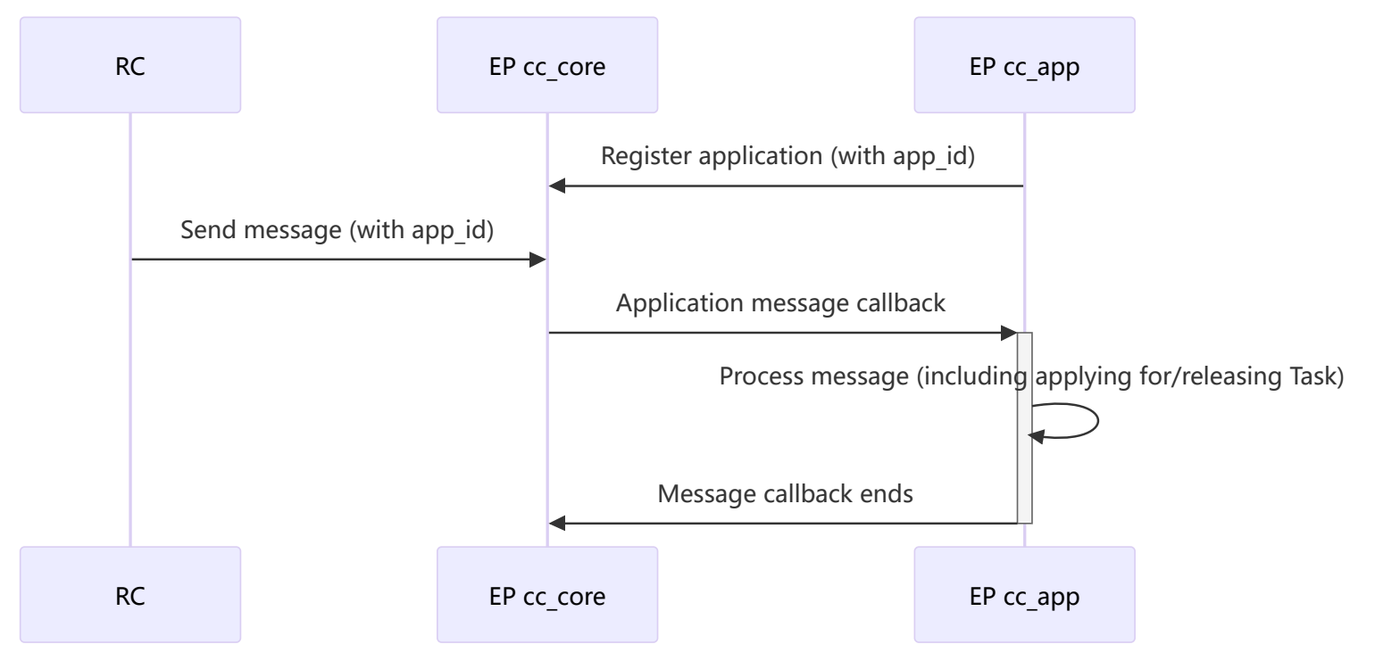
Original technical figure, page 27
6. Chips Connect Configuration
6.1 EP Card User-Level Device Driver
The EP Card User-Level Device Driver refers to the EP function driver running on the RC side, including kernel modules and user-level APPs.
6.1.1 Using-RC-DMA Mode
The Using-RC-DMA mode operates exclusively when the EP card is connected to RK RC devices, allowing the PCIe bandwidth to be maximized. By default, only the EP-side DMA is utilized. The principle of the Using-RC-DMA mode is to leverage the DMA on the RC side as well. When the EP writes data to the RC, it calls upon the EP’s DMA; when the RC writes data to the EP, it calls upon the RC’s DMA, without interference. The RC-side DMA is limited to transferring data to physical spaces that have memory inbound mapping to BAR. Therefore, BAR2 is allocated for RC DMA usage. The default size is 64M, which can be modified in the EP- side dts configuration. This memory is used only when the RC writes data to the EP, specifically during the initialization phase when the send_buff_size is configured, and it must not be smaller than send_buff_size . Enabling the Mode No modifications are required for the RC and EP device drivers; only the parameter configuration during the initialization phase of the RC upper-layer application is needed.
dev_attr.using_rc_dma = 1; //使⽤RC DMA
dev_attr.rc_dma_chn = 1; //通道1,⽀持0/1
After successful enabling, the following LOG can be observed in the RC application:
rk pcie version: v2.0.0 - 202300927
using rc dma: 1, chn: 1   //使能RC DMA,通道1
open rkrmd: /dev/pcie-rkep-0000:01:00.0 Success.
When the EP application creates a Task, the following LOG will be displayed:
task create id: 1
using rc dma: 1
Recommended Configuration Single EP scenario: It is recommended to enable using_rc_dma and configure it to Channel 0. Multiple EP scenarios: It is recommended to disable using_rc_dma, using the EP’s own DMA to transfer data, which can maintain a roughly equal transmission rate for each EP.
7. Typical Business Scenarios of Chips Connect
7.1 EP Video Acceleration Card
The video acceleration card transfers RC’s video stream to EP via the PCIE bus for decoding and processing, and then transmits it back to the main chip for display via the PCIE bus. The basic data flow processing is shown in the figure below:
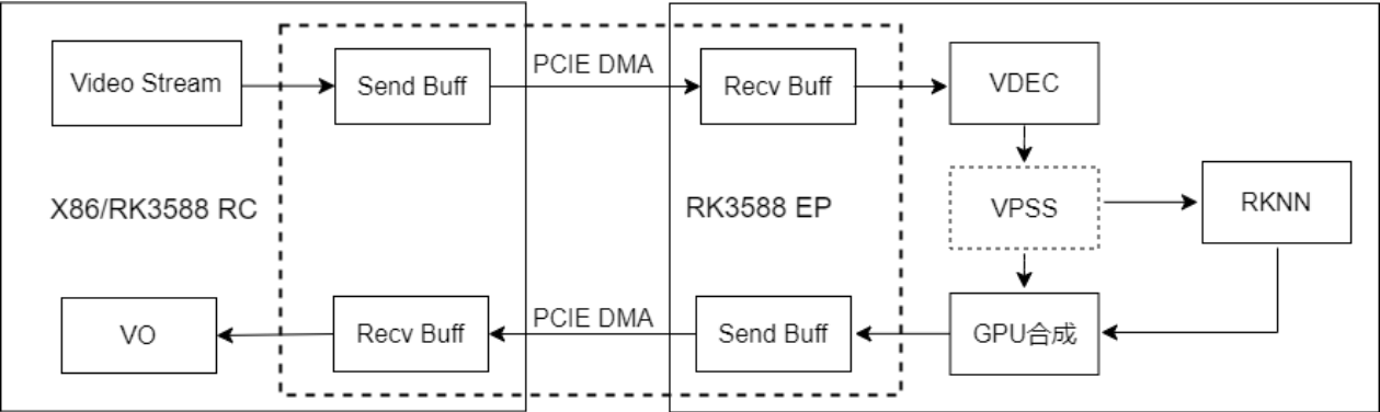
Original technical figure, page 29
The stream sender first obtains the stream data from the video stream, copies it into the prepared send stream buffer, and then sends the stream data to the recv stream buffer on the PCIE opposite end through PCIE DMA. The opposite end then extracts the stream and processes it through VDEC into VPSS, which outputs two streams of data. One stream is sent to the GPU for synthesis, and the other stream is sent to RKNN for processing. The synthesized data is copied into the prepared send stream buffer, and then the data is sent to the recv stream buffer on the PCIE opposite end through PCIE DMA. The opposite end extracts the data and sends it to the VO module for display. The SDK has implemented the stream buffers for both the sender and receiver, which can be used by configuring parameters during the initialization phase. Users only need to focus on the business process.
8. Chips Connect Acceptance Criteria
It is recommended to follow the process below to confirm that the software, hardware, and basic business processes are functioning correctly when using the PCIe EP development kit for the first time, before starting custom feature development.
8.1 Development Package List
Directory Structure Introduction
.
├── bootloader                    # pcie ep bootloader源码⼯程
├── build                         # build编译脚本
├── core
│   ├── api                       # sdk对外api,包含rc和ep
│   └── component                 # pcie组件,主要是负责buf管理,消息通知等
│   └── framework                 # 框架层,主要负责和OS交互,对上提供系统能⼒以及PCIE功能
├── docs                          # PCIE EP SDK⽂档介绍
├── examples
│   ├── pcie_camera_test          # EP卡典型业务,抓取EP Camera数据数据处理,仅android端使⽤
│   ├── pcie_speed_test           # EP卡典型业务,PCIE传输速率测试Demo
│   └── pcie_video_test           # EP卡典型业务,视频卡Demo
│   └── pcie_download_test        # EP卡RC下载固件启动⽅案Demo
│   └── pcie_auto_test            # EP卡功能⾃动化测试Demo
│   └── windows                   # EP卡Windows测试Demo
└── images                        # 功能验证固件
└── patch*                        # 补丁⽬录
└── third-party                   # 第三⽅依赖
Introduction to the main directories of the development package: The core/framework directory implements basic functions, including memory allocation management, logging functions, linked_list, DMA, PCIe CONFIG, and other RC and EP common components. framework/core/pcie: Implements DMA transfer, responsible for interacting with chip DMA configuration. framework/core/mem: Implements memory allocation and release under different configurations. framework/osal: Encapsulates the implementation of OS interfaces, shielding the differences between different OS from the upper layer. framework/base: Implements basic data structures, such as linked lists, queues, etc. The core/component directory encapsulates the implementation of RC and EP interfaces, internally implementing buf management, message notification, data transfer, etc., and externally providing specific APIs for development without calling through the OS. This directory consists of three parts: ep_pcie: Responsible for buf management, message notification, and data transfer related implementations for the PCIe EP part. rc_pcie: Responsible for buf management, message notification, and data transfer related implementations for the PCIe RC part. cc_pcie_type.h and cc_cmp_pcie_type.h: Provide unified data structures and data types for external communication between RC and EP. The core/api directory encapsulates the implementation of different system user interface layers, providing specific APIs for user development. This directory consists of four parts: ep: RK EP only needs to support the arm environment, so this part only encapsulates the component/ep_pcie interface without implementing additional logic. rc/windows: The Windows system is developed using driver forms, providing ioctl calls for users. rc/other: Other systems besides Windows do not need to use driver development, so this part only encapsulates the component/rc_pcie interface without implementing additional logic.
build: The directory implements the compilation and construction of the SDK, supporting Linux, Android, and Windows. docs: Standard EP board documentation. examples: Provides different test samples, sample introductions, and operation instructions. Please refer to the README in the corresponding directory. images: The directory contains firmware and samples that can be directly used for basic functional testing. patch: Patches corresponding to the SDK package, supporting Linux and Android systems. Patch instructions can be found in patch/README .
8.2 Patch Update One-Click Effectiveness for “Update Package” Source Code
Testing Objective Standard card driver version upgrade, supporting one-click addition of patches in the “Update Package” directory. Testing Method RK3588:
./ep_patch.sh release patch-kernel5.10/更新包 ./path-to-dst/
RK3568:
./ep_patch.sh release patch-kernel4.19/更新包 ./path-to-dst/
Additional Notes: Generating patch packages:
./ep_patch.sh release ./.. patch-kernel5.10/更新包
cd ./../kernel/
git checkout develop-4.19
cd -
./ep_patch.sh kernel ./.. patch-kernel4.19/更新包
8.3 Functional Key Log Information
8.3.1 Key lspci Information on RC Side
Confirm the following information: bar is enabled and properly allocated
MSI is enabled and properly allocated LnkCap, Gen3x4 support, ASPM not supported LnkSta, Gen3x4 status Kernel driver in use: pcie-rkep Log example:
01:00.0 Class 1200: Device 1d87:356a (rev 01)
        Control: I/O- Mem+ BusMaster+ SpecCycle- MemWINV- VGASnoop- ParErr- Stepping- SERR-
FastB2B- DisINTx+
        Status: Cap+ 66MHz- UDF- FastB2B- ParErr- DEVSEL=fast >TAbort- <TAbort- <MAbort-
>SERR- <PERR- INTx-
        Latency: 0
        Interrupt: pin A routed to IRQ 157
        Region 0: Memory at f0400000 (32-bit, non-prefetchable) [size=4M]
        Region 2: Memory at 900000000 (64-bit, prefetchable) [size=64M]
        Region 4: Memory at f0200000 (32-bit, non-prefetchable) [size=1M]
        Capabilities: [40] Power Management version 3
                Flags: PMEClk- DSI- D1+ D2+ AuxCurrent=375mA PME(D0+,D1+,D2-,D3hot+,D3cold-)
                Status: D0 NoSoftRst+ PME-Enable- DSel=0 DScale=0 PME-
        Capabilities: [50] MSI: Enable+ Count=4/32 Maskable+ 64bit+
                Address: 00000000fe670040  Data: 0000
                Masking: fffffff0  Pending: 00000000
        Capabilities: [70] Express (v2) Endpoint, MSI 08
                DevCap: MaxPayload 256 bytes, PhantFunc 0, Latency L0s unlimited, L1
unlimited
                        ExtTag+ AttnBtn- AttnInd- PwrInd- RBE+ FLReset- SlotPowerLimit
0.000W
                DevCtl: Report errors: Correctable- Non-Fatal- Fatal- Unsupported-
                        RlxdOrd+ ExtTag+ PhantFunc- AuxPwr- NoSnoop-
                        MaxPayload 256 bytes, MaxReadReq 256 bytes
                DevSta: CorrErr- UncorrErr- FatalErr- UnsuppReq- AuxPwr- TransPend-
                LnkCap: Port #0, Speed 8GT/s, Width x4, ASPM not supported, Exit Latency L0s
<4us, L1 <16us
                        ClockPM- Surprise- LLActRep- BwNot- ASPMOptComp+
                LnkCtl: ASPM Disabled; RCB 64 bytes Disabled- CommClk-
                        ExtSynch- ClockPM- AutWidDis- BWInt- AutBWInt-
                LnkSta: Speed 8GT/s, Width x4, TrErr- Train- SlotClk+ DLActive- BWMgmt-
ABWMgmt-
                DevCap2: Completion Timeout: Not Supported, TimeoutDis+, LTR+, OBFF Via
message/WAKE#
                DevCtl2: Completion Timeout: 50us to 50ms, TimeoutDis-, LTR+, OBFF Disabled
                LnkCtl2: Target Link Speed: 8GT/s, EnterCompliance- SpeedDis-
                         Transmit Margin: Normal Operating Range, EnterModifiedCompliance-
ComplianceSOS-
                         Compliance De-emphasis: -6dB
                LnkSta2: Current De-emphasis Level: -6dB, EqualizationComplete+,
EqualizationPhase1+
                         EqualizationPhase2+, EqualizationPhase3+, LinkEqualizationRequest-
        Capabilities: [b0] MSI-X: Enable- Count=128 Masked-
                Vector table: BAR=4 offset=00020000
                PBA: BAR=4 offset=00028000
        Capabilities: [100 v2] Advanced Error Reporting
                UESta:  DLP- SDES- TLP- FCP- CmpltTO- CmpltAbrt- UnxCmplt- RxOF- MalfTLP-
ECRC- UnsupReq- ACSViol-
                UEMsk:  DLP- SDES- TLP- FCP- CmpltTO- CmpltAbrt- UnxCmplt- RxOF- MalfTLP-
ECRC- UnsupReq- ACSViol-
                UESvrt: DLP+ SDES+ TLP- FCP+ CmpltTO- CmpltAbrt- UnxCmplt- RxOF+ MalfTLP+
ECRC- UnsupReq- ACSViol-
                CESta:  RxErr- BadTLP- BadDLLP- Rollover- Timeout- NonFatalErr-
                CEMsk:  RxErr- BadTLP- BadDLLP- Rollover- Timeout- NonFatalErr+
                AERCap: First Error Pointer: 00, GenCap+ CGenEn- ChkCap+ ChkEn-
        Capabilities: [148 v1] #19
        Capabilities: [168 v1] Address Translation Service (ATS)
                ATSCap: Invalidate Queue Depth: 00
                ATSCtl: Enable-, Smallest Translation Unit: 00
        Capabilities: [178 v1] Page Request Interface (PRI)
                PRICtl: Enable- Reset-
                PRISta: RF- UPRGI- Stopped+
                Page Request Capacity: 00000001, Page Request Allocation: 00000000
        Capabilities: [188 v1] Latency Tolerance Reporting
                Max snoop latency: 0ns
                Max no snoop latency: 0ns
        Capabilities: [190 v1] L1 PM Substates
                L1SubCap: PCI-PM_L1.2+ PCI-PM_L1.1+ ASPM_L1.2+ ASPM_L1.1+ L1_PM_Substates+
                          PortCommonModeRestoreTime=10us PortTPowerOnTime=10us
        Capabilities: [1a0 v1] #16
        Capabilities: [1d0 v1] Vendor Specific Information: ID=0002 Rev=4 Len=100 <?>
        Capabilities: [2d0 v1] Vendor Specific Information: ID=0006 Rev=0 Len=018 <?>
        Capabilities: [2e8 v1] #15
        Kernel driver in use: pcie-rkep
8.3.2 EP-side spl.bin Boot Log
Verify the following information: Kernel phase prints “already linkup” Log example:
... #spl关键打印

U-Boot SPL board init
RKEP: Init PCIe EP
RKEP: 188259 - PHY Mode 0x4
RKEP: 189537 - RKEP: GRF:904=7, a04=7...
RKEP: 190138 - RKEP: GRF:904=7, a04=f...
RKEP: 190487 - RKEP: GRF:904=f, a04=f...
RKEP: 190827 - RefClock in common clock_mode
RKEP: 200593 - BAR0: 0x3c000000
RKEP: 200864 - BAR2: 0x010000000
RKEP: 201247 - init PCIe fast Link up
RKEP: 218243 - Link up 230011
RKEP: 259699 - Done

... #内核关键打印

[00-06-34.831][    3.148198] rk-pcie-ep fe150000.pcie: bar0: assigned [0x3c000000-3c3fffff]
[00-06-34.834][    3.149015] rk-pcie-ep fe150000.pcie: bar2: assigned [0x40000000-43ffffff]
[00-06-34.834][    3.149027] rk-pcie-ep fe150000.pcie: no vpcie3v3 regulator found
[00-06-34.837][    3.149046] rk-pcie-ep fe150000.pcie: already linkup
[00-06-34.837][    3.149320] rk-pcie-ep fe150000.pcie: register misc device pcie_ep
8.3.3 EP End PCIe.bin Boot Log
Confirm the following information: Record the running time of pcie.bin
| Version | Duration |
|---|---|
| V1.00 | 360ms |
SPL phase prints “already link up” Kernel phase prints “already linkup” Log example:
#pcie.bin关键打印
PCIe_EP Release Time: Jan  2 2025 V2.20
Gen3x4
phyMode4
HW
controlelr initialed
GRF:904=0007, a04=0007...
GRF:904=004F, a04=004F...
phy locked
phy initialed
vid=0x1D87 did=0x356A
ms=000C
Linking, ltssm:
00000001
00000002
00000007
00210022
00210023
00230011
Link up
rst_fun1
Link stable, ltssm
00230011
out

... #spl关键打印

U-Boot SPL board init
RKEP: Init PCIe EP
RKEP: already link up

... #内核关键打印

[00-06-34.831][    3.148198] rk-pcie-ep fe150000.pcie: bar0: assigned [0x3c000000-3c3fffff]
[00-06-34.834][    3.149015] rk-pcie-ep fe150000.pcie: bar2: assigned [0x40000000-43ffffff]
[00-06-34.834][    3.149027] rk-pcie-ep fe150000.pcie: no vpcie3v3 regulator found
[00-06-34.837][    3.149046] rk-pcie-ep fe150000.pcie: already linkup
[00-06-34.837][    3.149320] rk-pcie-ep fe150000.pcie: register misc device pcie_ep
8.4 Functionality Firmware Burning
Please refer to the “Single EP Card Interface Universal RC” section to confirm whether it is a product form that requires a quick start, and confirm the storage solution used and perform the corresponding PC upgrade burning verification, mainly including: Single Storage Dual Storage EP Boot For detailed information, refer to the “EP Card Firmware Compilation” section.
8.5 Performance User-Space Test Demo - PCIe Speed Test
8.5.1 Testing Objectives
Verify the business fundamentals, which mainly include: Wired DMA to EP transfer on the RC side, DMA transfer rate, and bidirectional DMA transfer Local DMA to RC transfer on the RC side, DMA transfer rate, and bidirectional DMA transfer BAR mapping, normal access ELBI operates normally, supporting RC to trigger interrupt event notifications to EP MSI operates normally, supporting EP to trigger interrupt event notifications to RC Based on requirements, verify: If a DMA-supported RK RC is selected, it supports Local DMA to EP transfer on the RC side, and DMA transfer rate Firmware download
8.5.2 Testing Method
For detailed reference, please consult the document examples/pcie_speed_test/README.md.
8.5.3 RK3588 Gen3x4 Test Results
Test Equipment RC: RK3588-EVB1-LP4X-V10 PCIe 3.0 4 lanes with main core at 2.4G and auxiliary core at 1.8G, CPU/Dram set to high frequency EP: RK3588-EVB4-LP4X-V10 PCIe 3.0 4 lanes with main core at 2.4G and auxiliary core at 1.8G, CPU/Dram set to high frequency Standard EP Version Rockchip_PCIE_EP_Standard_Card_20231215.tar.gz Test Parameters: Utilizing EP DMA engine task_num = 1 Test Results
| DMA Size | 64B | 256B | 4K | 64KB | 1MB | 4MB |
|---|---|---|---|---|---|---|
| RC Read (DMA Write) | 0.16MB/S | 0.65MB/S | 10.4MB/S | 165.8MB/S | 1898.7MB/S | 3271.3MB/s |
| RC Write (DMA Read) | 0.17MB/S | 0.73MB/S | 11.0MB/S | 171.1MB/S | 1630.6MB/S | 1735.6MB/s |
Explanation: If the test is initiated by RC and uses the default EP DMA engine, the write test is effectively an EP DMA read, and the read test is effectively an EP DMA write. The smaller the test granularity, the more scheduling is involved, leading to poorer performance, but overall performance can be improved by using multi-threading.
8.5.4 RK3588 Gen2x1 Test Results
Test Equipment RC: RK3588-EVB1-LP4X-V10 PCIe 3.0 4 lanes with 2.4G for the main core and 1.8G for the small core. EP: RK3588-EVB4-LP4X-V10 PCIe 3.0 4 lanes (reduced to Gen2 1 lane) with 2.4G for the main core and 1.8G for the small core. Standard EP Version Rockchip_PCIE_EP_Standard_Card_20231215.tar.gz Test Parameters:
Utilizing EP DMA engine task_num = 1 Test Results
| DMA Size | 64B | 256B | 4K | 64KB | 1MB | 4MB |
|---|---|---|---|---|---|---|
| Write | 0.16MB/S | 0.64MB/S | 10.2MB/S | 147.6MB/S | 394.0MB/S | 396.2MB/s |
| Read | 0.17MB/S | 0.70MB/S | 11.0MB/S | 149.2MB/S | 384.0MB/S | 384.1MB/s |
Explanation: If the test is initiated by RC and uses the default EP DMA engine, the write test actually corresponds to EP DMA read, and the read test actually corresponds to EP DMA write. The smaller the test granularity, the more scheduling is involved, leading to poorer performance, but overall performance can be improved by utilizing multi-threading.
8.5.5 RK1820 Gen2x1 Test Results
Test Equipment RC: RK3588-EVB1-LP4X-V10 PCIe 3.0 4 lanes, big core 2.4G, little core 1.8G EP: RK1820 PCIe 2.0 1 lane Standard EP Version RC - Rockchip_PCIE_EP_Standard_Card_20250523_V3.1.0.tar.gz EP - RK RT-Thread SDK develop-v5.1.x branch Test Parameters: Using EP DMA engine task_num = 1 RK1820 DRAM Memory Test Results
| DMA Size | 64B | 256B | 4K | 8K | 64KB | 512KB |
|---|---|---|---|---|---|---|
| RC Write (EP DMA Read) | 3MB/S | 10MB/S | 136MB/S | 188MB/s | 303MB/s | 317MB/s |
| RC Read (EP DMA Write) | 3MB/S | 11MB/S | 143MB/S | 237MB/S | 363MB/s | 382MB/s |
Explanation: If the test is initiated by RC and uses the default EP DMA engine, the write test is actually EP DMA read, and the read test is actually EP DMA write. The smaller the test granularity, the more scheduling is involved, the worse the performance, but overall performance can be improved by opening multiple threads. Compared to EP Linux OS, RT-Thread OS is a real-time system, allowing user-level programs to quickly
respond to interrupts, so small granularity data transfer still maintains a high throughput.
8.6 Performance User Space Test Demo - PCIe Loopback Test
8.6.1 Test Objective
Count the typical packet sending and receiving scenarios, and measure the response time duration of the serial process.
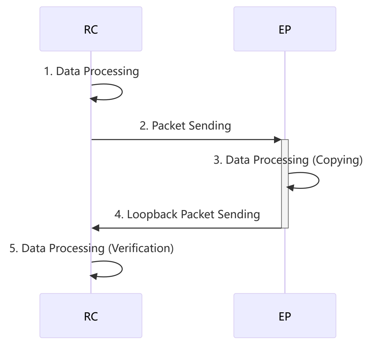
Original technical figure, page 38
8.6.2 Testing Method
For detailed reference, please consult the document located at examples/pcie_speed_test/README.md.
8.6.3 RK3588 Gen2x1 Test Results
Test Equipment RC: RK3588-EVB1-LP4X-V10 PCIe 3.0 4 lanes with main core at 2.4G and secondary core at 1.8G
EP: RK3588-EVB4-LP4X-V10 PCIe 3.0 4 lanes (reduced to Gen2 1 lane) with main core at 2.4G and secondary core at 1.8G Standard EP Version Rockchip_PCIE_EP_Standard_Card_20231215.tar.gz Test Parameters: Utilizing EP DMA engine task_num = 1 Test Results
| DMA Size | 4K |
|---|---|
| min/max | 105us/724us |
Explanation: If the test is initiated by RC and the default EP DMA engine is used, the write test is effectively an EP DMA read, and the read test is effectively an EP DMA write. The test results are statistical values after 1 second of testing, excluding the bias effects of the initialization process. The test results represent the best case scenario under continuous packet transmission; adjust intervals and other loads as needed to construct a worst case scenario.
8.6.4 RK1820 Gen2x1 Test Results
Test Equipment RC: RK3588-EVB1-LP4X-V10 PCIe 3.0 4 lanes with main core at 2.4G and secondary core at 1.8G EP: RK1820 PCIe 2.0 1 lane Standard EP Version RC - Rockchip_PCIE_EP_Standard_Card_20250523_V3.1.0.tar.gz EP - RK RT-Thread SDK develop-v5.1.x branch Test Parameters: Utilizing EP DMA engine task_num = 1 RK1820 DRAM Memory Test Results
| DMA Size | 4K |
|---|---|
| min/max | 83us/139us |
Notes:
If the test is initiated by RC and uses the default EP DMA engine, the write test actually corresponds to EP DMA read, and the read test corresponds to EP DMA write. The test results are statistical values after 1 second of testing, excluding the bias influence of the initialization process. The test results represent the best case scenario under continuous packet transmission; please adjust the gaps and other loads according to requirements to construct the worst case scenario.
8.7 Compatibility Enumeration
Test Objective Validate the compatibility and robustness of EP board detection, identification, and enumeration on different RCs. Test Method RK EP primarily interfaces with RCs:
| EP Device | RC Device | Cold Boot |
Wake from Suspend |
Hot Boot |
Confirmation Method |
|---|---|---|---|---|---|
| RK3588 EVB4 V11 |
RK3588 EVB1 V10 |
20/20 | 20/20 | 20/20 | Linux: lspci | grep 356a |
| RK3588 EVB4 V11 |
PC ubuntu | 20/20 | 20/20 | 20/20 | Linux: lspci | grep 356a |
| RK3588 EVB4 V11 |
PC windows | 20/20 | 20/20 | 20/20 | Device Manager to confirm corresponding devices |
| RK3568 iotest device |
RK3588 EVB1 V10 |
20/20 | 20/20 | 20/20 | Linux: lspci | grep 356a |
| RK3568 iotest device |
PC ubuntu | 20/20 | 20/20 | 20/20 | Linux: lspci | grep 356a |
Notes: Actual products should cover as many target RC devices as possible. Cold Boot: PC power off, power on, press the POWER button. Wake from Suspend: RK RC: Enter and exit suspend with the POWER button. Ubuntu: Desktop versions can enter through the interface buttons, other scenarios to be confirmed. Windows: CTRL+L key combination to enter, other scenarios to be confirmed. Hot Boot: RK3588: Enter root privileges, input the reboot command in the shell interface.
Ubuntu: Enter root privileges, input the reboot command in the shell interface. Windows: Under the desktop, ALT+F4 key combination to pop up reset options, select reset, some PCs support direct power button reset.
8.8 Compatibility EP Reset and RC Re-enumeration Detection
Test Objective Test the robustness of the business under the scenario of “EP standalone reset”, focusing on the following aspects: PCIe remove/rescan functionality Whether communication is restored normally Whether the business is thriving Test Method The following tests should be conducted under the condition that the above-mentioned functional tests are all normal, and compile the executable file of examples/pcie_auto_test, refer to the examples/pcie_auto_test/README.md document to deploy the test environment. PCIe remove/rescan functionality Execute ./pcie_auto_test_rc 2 0 and ./pcie_auto_test_rc 3 0 on the RC side to select the 0th device for Remove and Rescan operations. Whether communication is restored normally Whether the business is thriving Execute ./pcie_auto_test_rc 0 0 on the RC side to select the 0th device for API stability operations.
8.9 Functional OTA
Please refer to the “Single EP Card Universal RC” section to confirm whether it is a product form that requires quick startup, and confirm the storage solution used and perform corresponding OTA verification, mainly including: Single Storage Dual Storage EP Boot For detailed reference, please see the “EP Card OTA” section.
9. Chips Connect Exception Handling
9.1 RC-side x86 Platform Initialization of PCIe Reports mmap Failed, Operation Not Permitted
root@rk:/home/rc-sample# ./pcie_test 10240
resource path = /sys/bus/pci/devices/0000:01:00.0/enable
resource path = /sys/bus/pci/devices/0000:01:00.0/resource0
mmap failed, ret = 0, Operation not permitted
ep dev num : 1
Segmentation fault (core dumped)
Answer: This issue arises because Ubuntu, starting from version 20.04, has introduced a Linux kernel lockdown feature. If Secure Boot is enabled in the BIOS, it activates the kernel lockdown, leading to mmap failure. To resolve this, one must enter the BIOS and disable Secure Boot to proceed normally.
9.2 HugePage Configuration
The RK platform supports Hugepage sizes of 2M, 32M, and 1GB, while other platforms support sizes based on the actual system. The configuration for a single Hugepage size must be larger than the size of a single send buffer and a single receive buffer in the SDK, and the number of Hugepages must exceed the required Buff quantity. For example: 5 send Buffs, with each Buff being 4M, and 5 receive Buffs, with each Buff being 8M. In this case, it is not possible to configure Hugepage as 2M; the minimum configuration required is 32M. The number of Hugepages needed for send Buffs = (int) (5 / (32M / 4M)) + 1 = 1 The number of Hugepages needed for receive Buffs = (int) (5 / (32M / 8M)) + 1 = 2 The final configuration would be default_hugepagesz=32M, hugepagesz=32M, hugepages=3
9.2.1 X86 Platform
Check the size of Hugepagesize
rk@debian:~$ cat /proc/meminfo | grep Huge
HugePages_Total:       2
HugePages_Free:        2
HugePages_Rsvd:        0
HugePages_Surp:        0
Hugepagesize:    2048 kB
Hugetlb:         4096 kB
Modify the size to 1GB
Modify the cmdline parameter, edit /etc/default/grub, add default_hugepagesz=1G
GRUB_CMDLINE_LINUX_DEFAULT="quiet default_hugepagesz=1G hugepagesz=1G hugepages=1"
GRUB_CMDLINE_LINUX=""
Generate the configuration
/usr/sbin/grub-mkconfig -o /boot/grub/grub.cfg
Restart the device reboot or systemctl poweroff Check the size and count, cat /proc/meminfo | grep Hugepagesize
rk@debian:~$ cat /proc/meminfo | grep Huge
HugePages_Total:       1
HugePages_Free:        1
HugePages_Rsvd:        0
HugePages_Surp:        0
Hugepagesize:    1048576 kB
Hugetlb:         1048576 kB
9.2.2 RK Platform
Kernel Enabling Hugepage Configuration
+++ b/arch/arm64/configs/rockchip_linux_defconfig
@@ -1,5 +1,10 @@
 CONFIG_DEFAULT_HOSTNAME="localhost"
 CONFIG_SYSVIPC=y
+CONFIG_HUGETLBFS=y
 CONFIG_NO_HZ=y
 CONFIG_HIGH_RES_TIMERS=y
 CONFIG_PREEMPT_VOLUNTARY=y
Configuring the Default Size and Number of Hugepages: Add three properties default_hugepagesz=32M hugepagesz=32M hugepages=16 to the cmdline, configuring Hugepages to be 32M in size and the number available to be 16.
+++ b/arch/arm64/boot/dts/rockchip/rk3588-linux.dtsi
@@ -6,7 +6,7 @@

 / {
        chosen: chosen {
-               bootargs = "earlycon=uart8250,mmio32,0xfeb50000 console=ttyFIQ0 irqchip.gicv3_pseudo_nmi=0 clk_gate.always_on=1 pm_domains.always_on=1 root=PARTUUID=614e0000-0000 rw rootwait";
+               bootargs = "earlycon=uart8250,mmio32,0xfeb50000 console=ttyFIQ0 irqchip.gicv3_pseudo_nmi=0 clk_gate.always_on=1 pm_domains.always_on=1 root=PARTUUID=614e0000-0000 rw rootwait default_hugepagesz=32M hugepagesz=32M hugepages=16";
        };

        cspmu: cspmu@fd10c000 {
Recompile the kernel and flash it. After booting, check /proc/meminfo to confirm if it has been added successfully.
[root@RK3588:/userdata]# cat /proc/meminfo | grep Huge
HugePages_Total:      16
HugePages_Free:       16
HugePages_Rsvd:        0
HugePages_Surp:        0
Hugepagesize:      32768 kB
Hugetlb:         1048576 kB
9.3 Encountering Kernel Errors or Bus Errors After Operating on the user cmd Area or ep info Area via API Interfaces
There are two main reasons that could lead to this issue:
-
Utilizing interfaces such as memset or memcpy to manipulate this block of memory.
-
The application’s compilation optimization level exceeds -O1. In the first scenario, review the code to remove interfaces like memset or memcpy and instead use a for loop for manipulation.
In the second scenario, you can reduce the optimization level or add the compilation parameter -fno-tree-loop-optimize to disable loop optimization.
9.4 Building the Windows Driver Compilation Environment
Current driver development and verification platform: System Version Windows 10 2004, WDK Version 10.0.19041.685.
- Confirm System Version
Right-click on the computer properties to check the system version or press Win+R and enter winver to view, focusing mainly on the operating system internal version: 19042.1052.
版本                Windows 10 专业版
版本号              20H2
安装⽇期            2021/6/5
操作系统内部版本     19042.1052
-
Download and install VS2019 and WDK, refer to online tutorials for guidance.
-
Disable driver signature enforcement on the Windows host, here are three methods provided: Advanced Startup Options: Restart the computer and enter the advanced startup options during the boot process (usually requires pressing F8 at startup). In the advanced startup options menu, if you see “Disable driver signature enforcement” or a similar option, and this option is selected, then digital signature verification is turned off. Using Command Prompt (only for temporary disablement): Open Command Prompt (as administrator). Enter the following command: bcdedit /set testsigning on Using Local Group Policy Editor (applicable for Windows Pro and higher versions): Open “Local Group Policy Editor” (gpedit.msc). Navigate to “Computer Configuration” -> “Administrative Templates” -> “System” -> “Driver Installation”. Review the setting for “Device: Allow installation of unsigned drivers”. If this setting is enabled, it means that digital signature verification may be disabled. Restart the computer, if you see the words “Test Mode” in the bottom right corner of the desktop, this indicates that digital signature verification is disabled. If digital signatures are not disabled, the driver will fail to install.
-
Load Project Compilation The VS project file is located in the build/windows/rk_projects directory, simply open the rk_projects.sln. The project rc_pcie is the driver project, supporting 4 configurations (different configurations are due to some APIs being deprecated after Windows 10 2004 version, requiring isolation through configurations): Debug_eq_win10_2004 : Debug environment, for systems greater than Windows 10 2004 Debug_less_win10_2004 : Debug environment, for systems less than or equal to Windows 10 2004 Release_eq_win10_2004 : Release environment, for systems greater than Windows 10 2004 Release_less_win10_2004 : Release environment, for systems less than or equal to Windows 10 2004 The project examples is the test project, supporting Debug and Release configurations, used to verify if the driver is functioning properly. After successful compilation, the driver and test files will be output in the build/windows/rk_projects/x64 directory.
9.5 Windows Application Execution Error: MSVCP140.dll and vcruntime140.dll Not Found
Download and install Visual C++ Redistributable for Visual Studio 2015
9.6 Error Occurs When Attempting to Modify Debug Program Settings in Windows Debugging Mode. The value is protected by Secure Boot policy and cannot be modified or deleted
Enter Windows 10 BIOS and disable Secure Boot by setting “secure boot” to “disable”.
10. Chips Connect API Reference
For detailed reference, please consult the document Rockchip_Developer_Guide_PCIE_EP_Standard_Card_APIs.