
This complete technical reference follows Rockchip V1.2.0. The source scope is RK3576 / RK3506 / RV1126B, kernel 6.10. It is an ArmSoM platform reference: verify the actual board, SoC, SDK/BSP branch, kernel and peripheral configuration. No board-level hardware validation has been performed; support on every ArmSoM board is not implied.
Chinese follows the 17-page Chinese PDF; English follows the 19-page English PDF and Russian fully translates its technical text. Chinese uses Chinese-source figures; English and Russian use English-PDF figures, including any Chinese UI labels present in those originals. Source conflicts and extraction repairs are recorded in the editorial notes. Code comments and output retain their source language.
Operational risk: DSMC mappings, direct memory access and DMA can cause bus exceptions, data loss or boot failure. Addresses, timings and code are retained as source examples; verify the actual schematic, slave capacity, power/initialization sequence and SDK. The source kernel 6.10 is not silently changed to another version. Code issues requiring verification are recorded in the editorial notes. No hardware reads or writes were executed.
Official resources: ArmSoM、Rockchip Linux。
| SoC | Kernel |
|---|---|
| RK3576 / RK3506 / RV1126B | kernel 6.10 |
1. Terminology
DSMC: Double Data Rate Serial Memory Controller.
PSRAM: Pseudo static random access memory.
DPRAM: Dual Port Random Access Memory.
2. Overview
The Double Data Rate Serial Memory Controller(DSMC) features high bandwidth with fewer pins by time- division multiplexing the command, address, and data lines, with data transmitted on both the rising and falling edges. The data width supports x8, x16, and up to 4 chip selects. The protocol supports Hyperbus PSRAM, Xccela PSRAM, and Local bus. If using the Local bus protocol, the slave device must use the rockchips designed slave model or a device with a similar transmission protocol. If using HYPERBUS PSRAM or XCCELA PSRAM protocols, the slave device supports PSRAM chips from manufacturers such as Winbond, AP Memory, Cypress, and ISSI.
3. DSMC Driver
3.1 Driver Files
The DSMC driver file locations:
drivers/memory/rockchip/dsmc-host.c /* Main driver program */
drivers/memory/rockchip/dsmc-controller.c /* The DSMC controller behavior configuration */
drivers/memory/rockchip/dsmc-lb-device.c /* The DSMC Local bus device */
3.2 DTS Configuration
    dsmc: dsmc@2a280000 {
        ...
        clock-frequency = <100000000>; /* DSMC interface frequency */
        ...
        /* Slave device properties */
        slave {
            rockchip,dqs-dll = <0x20 0x20 /* DQS0, DQS1 DLL delay for slave device cs0
*/
                   0x20 0x20 /* DQS0, DQS1 DLL delay for slave device cs1
*/
                   0x20 0x20 /* DQS0, DQS1 DLL delay for slave device cs2
*/
                   0x20 0x20>; /* DQS0, DQS1 DLL delay for slave device cs3
*/
            /*
             * rockchip,ranges: Base address and size of DSMC access to slave device memory;
             * If different CS have different memory space sizes, configure the largest.
             * rockchip,ranges = <0x0 0x10000000 0x0 0x2000000> means that if the slave is
             * PSRAM, allocate 0x2000000 memory size for each CS;
             * If the slave is Local Bus, allocate 0x2000000 memory size for each region
             */
            rockchip,ranges = <0x0 0x10000000 0x0 0x2000000>;
            rockchip,slave-dev = <&dsmc_slave>;
        };
    };
    dsmc_slave: dsmc_slave {
        compatible = "rockchip,dsmc-slave";
        rockchip,clk-mode = <0>; /* Clock mode, only for Local bus */
        status = "disabled";
        /*
         * Enable the corresponding slave device cs nodes when the slave
         * device is PSRAM (Hyperbus Psram or Xccela Psram).
         */
        psram {
            /*
             * When using PSRAM, there is no need to specify the bit width as
             * the driver automatically adapts it.
             */
            psram0 {
                status = "disabled"; /* If the slave device cs0 is PSRAM, change to "okay"
*/
            };
            psram1 {
                status = "disabled"; /* If the slave device cs1 is PSRAM, change to "okay"
*/
            };
            psram2 {
                status = "disabled"; /* If the slave device cs2 is PSRAM, change to "okay"
*/
            };
            psram3 {
                status = "disabled"; /* If the slave device cs3 is PSRAM, change to "okay"
*/
            };
        };
        /* Enable and configure the corresponding nodes if the slave is a Local bus device
*/
        lb-slave {
            rockchip,io-width = <16>; /* The data width of the local bus slave */
            dsmc_lb_slave0: lb-slave0 {
                rockchip,mtr-timing = <1 0 0 0 0 0 2 2>; /* The core timing, modifiable
according to slave design */
                rockchip,int-en = <0x0>; /* The current cs uses the interrupt sequence
number on the pin */
                status = "disabled";/* If the cs0 slave is a Local bus, change to "okay" */
                dsmc_p0_region: region {
                    dsmc_p0_region0: region0 {/* Attributes of this slave region0 */
                        rockchip,attribute = "Merged FIFO";/* The region0 is merged FIFO */
                        rockchip,ca-addr-width = <0>;/* CA transfer format, 0: 32bit, 1:
16bit */
                        rockchip,dummy-clk-num = <1>;/* Write transfer dummy clk cycle
number */
                        rockchip,cs0-be-ctrled = <0>;/* cs0 is controlled by cs1, cs2, cs3
*/
                        rockchip,cs0-ctrl = <0>; /* cs0 controls cs1, cs2, cs3 */
                        status = "disabled";
                    };
                    dsmc_p0_region1: region1 {/* Attributes of this slave region1 */
                        rockchip,attribute = "No-Merge FIFO";/* region1 is unmerged FIFO */
                        rockchip,ca-addr-width = <0>;
                        rockchip,dummy-clk-num = <1>;
                        rockchip,cs0-be-ctrled = <0>;
                        rockchip,cs0-ctrl = <0>;
                        status = "disabled";
                    };
                    dsmc_p0_region2: region2 {/* Attributes of this slave region2 */
                        rockchip,attribute = "DPRA";/* region2 is DPRAM */
                        rockchip,ca-addr-width = <0>;
                        rockchip,dummy-clk-num = <1>;
                        rockchip,cs0-be-ctrled = <0>;
                        rockchip,cs0-ctrl = <0>;
                        status = "disabled";
                    };
                    dsmc_p0_region3: region3 {/* Attributes of this slave region3 */
                        rockchip,attribute = "Register";/* region3 is register */
                        rockchip,ca-addr-width = <0>;
                        rockchip,dummy-clk-num = <1>;
                        rockchip,cs0-be-ctrled = <0>;
                        rockchip,cs0-ctrl = <0>;
                        status = "disabled";
                    };
                };
            };
            dsmc_lb_slave1: lb-slave1 {
                rockchip,mtr-timing = <1 0 0 0 0 0 2 2>; /* The core timing, modifiable
according to slave design */
                rockchip,int-en = <0x1>; /* The current cs uses the interrupt sequence
number on the pin */
                status = "disabled";/* If cs1 slave is a Local bus, change to "okay" */
                dsmc_p1_region: region {
                    dsmc_p1_region0: region0 {
                        rockchip,attribute = "Merged FIFO";
                        rockchip,ca-addr-width = <0>;
                        rockchip,dummy-clk-num = <1>;
                        rockchip,cs0-be-ctrled = <0>;
                        rockchip,cs0-ctrl = <0>;
                        status = "disabled";
                    };
                    dsmc_p1_region1: region1 {
                        rockchip,attribute = "No-Merge FIFO";
                        rockchip,ca-addr-width = <0>;
                        rockchip,dummy-clk-num = <1>;
                        rockchip,cs0-be-ctrled = <0>;
                        rockchip,cs0-ctrl = <0>;
                        status = "disabled";
                    };
                    dsmc_p1_region2: region2 {
                        rockchip,attribute = "DPRA";
                        rockchip,ca-addr-width = <0>;
                        rockchip,dummy-clk-num = <1>;
                        rockchip,cs0-be-ctrled = <0>;
                        rockchip,cs0-ctrl = <0>;
                        status = "disabled";
                    };
                    dsmc_p1_region3: region3 {
                        rockchip,attribute = "Register";
                        rockchip,ca-addr-width = <0>;
                        rockchip,dummy-clk-num = <1>;
                        rockchip,cs0-be-ctrled = <0>;
                        rockchip,cs0-ctrl = <0>;
                        status = "disabled";
                    };
                };
            };
            dsmc_lb_slave2: lb-slave2 {
                rockchip,mtr-timing = <1 0 0 0 0 0 2 2>; /* The core timing, modifiable
according to slave design */
                rockchip,int-en = <0x2>; /* The current cs uses the interrupt sequence
number on the pin */
                status = "disabled";/* If cs2 slave is a Local bus, change to "okay" */
                dsmc_p2_region: region {
                    dsmc_p2_region0: region0 {
                        rockchip,attribute = "Merged FIFO";
                        rockchip,ca-addr-width = <0>;
                        rockchip,dummy-clk-num = <1>;
                        rockchip,cs0-be-ctrled = <0>;
                        rockchip,cs0-ctrl = <0>;
                        status = "disabled";
                    };
                    dsmc_p2_region1: region1 {
                        rockchip,attribute = "No-Merge FIFO";
                        rockchip,ca-addr-width = <0>;
                        rockchip,dummy-clk-num = <1>;
                        rockchip,cs0-be-ctrled = <0>;
                        rockchip,cs0-ctrl = <0>;
                        status = "disabled";
                    };
                    dsmc_p2_region2: region2 {
                        rockchip,attribute = "DPRA";
                        rockchip,ca-addr-width = <0>;
                        rockchip,dummy-clk-num = <1>;
                        rockchip,cs0-be-ctrled = <0>;
                        rockchip,cs0-ctrl = <0>;
                        status = "disabled";
                    };
                    dsmc_p2_region3: region3 {
                        rockchip,attribute = "Register";
                        rockchip,ca-addr-width = <0>;
                        rockchip,dummy-clk-num = <1>;
                        rockchip,cs0-be-ctrled = <0>;
                        rockchip,cs0-ctrl = <0>;
                        status = "disabled";
                    };
                };
            };
            dsmc_lb_slave3: lb-slave3 {
                rockchip,mtr-timing = <1 0 0 0 0 0 2 2>; /* The core timing, modifiable
according to slave design */
                rockchip,int-en = <0x3>; /* The current cs uses the interrupt sequence
number on the pin */
                status = "disabled";/* If cs3 slave is a Local bus, change to "okay" */
                dsmc_p3_region: region {
                    dsmc_p3_region0: region0 {
                        rockchip,attribute = "Merged FIFO";
                        rockchip,ca-addr-width = <0>;
                        rockchip,dummy-clk-num = <1>;
                        rockchip,cs0-be-ctrled = <0>;
                        rockchip,cs0-ctrl = <0>;
                        status = "disabled";
                    };
                    dsmc_p3_region1: region1 {
                        rockchip,attribute = "No-Merge FIFO";
                        rockchip,ca-addr-width = <0>;
                        rockchip,dummy-clk-num = <1>;
                        rockchip,cs0-be-ctrled = <0>;
                        rockchip,cs0-ctrl = <0>;
                        status = "disabled";
                    };
                    dsmc_p3_region2: region2 {
                        rockchip,attribute = "DPRA";
                        rockchip,ca-addr-width = <0>;
                        rockchip,dummy-clk-num = <1>;
                        rockchip,cs0-be-ctrled = <0>;
                        rockchip,cs0-ctrl = <0>;
                        status = "disabled";
                    };
                    dsmc_p3_region3: region3 {
                        rockchip,attribute = "Register";
                    rockchip,ca-addr-width = <0>;
                    rockchip,dummy-clk-num = <1>;
                    rockchip,cs0-be-ctrled = <0>;
                    rockchip,cs0-ctrl = <0>;
                    status = "disabled";
                };
            };
        };
    };
};
Based on the type of the actual slave device, the user needs to enable the corresponding node. For PSRAM devices, the corresponding psramx node should be enabled based on the sequential number of the CS connected to the PCB. Whether it is Hyperbus or Xccela PSRAM, it will be automatically detected by the driver. When the slave device is an RK-designed DSMC slave, the corresponding lb_slavex node should be enabled based on the sequential number of the CS connected to the PCB. Additionally, the configuration of the corresponding region needs to be modified according to the attributes of the slave device. The clk-mode parameter controls the three supported clock behaviors: The clk-mode = 0 indicates no clock during CS high level, but clock is present during CS low level; The clk-mode = 1 indicates the clock is always present regardless of CS changes, allowing the slave device to use it as a reference clock. However, in this mode, high- frequency operation is not possible and various adjustable AC timing parameters are not available. The clk- mode = 2 indicates that there is a clock during both CS high and low levels, but several clocks will be disabled before and after the CS transition edge.
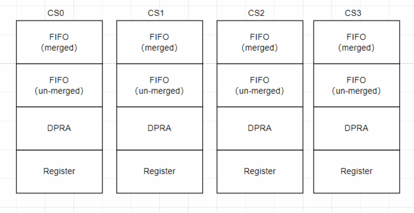
For the Local bus device, memory space is as follows:
Editable transcription of the figure:
| Region | CS0 | CS1 | CS2 | CS3 |
|---|---|---|---|---|
| 0 | FIFO (merged) | FIFO (merged) | FIFO (merged) | FIFO (merged) |
| 1 | FIFO (un-merged) | FIFO (un-merged) | FIFO (un-merged) | FIFO (un-merged) |
| 2 | DPRA | DPRA | DPRA | DPRA |
| 3 | Register | Register | Register | Register |
Each slave device’s chip select (CS) access space can be divided into 1, 2, or 4 regions (equally divided). Only the corresponding “status” attribute of the region needs to be enabled in the Device Tree Source (DTS) file.
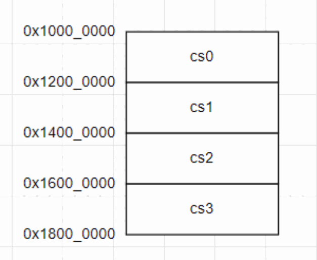
For the rockchip,ranges property, such as rockchip,ranges = <0x0 0x10000000 0x0 0x2000000> it configures the starting address and size of the memory space in the slave device. The meaning of these values varies depending on the type of peripheral.
If the slave is PSRAM, the rockchip,ranges property configures the size of the maximum CS space. The memory space division for each CS is as follows:
Editable transcription of the figure:
| CS | Start boundary | Next boundary |
|---|---|---|
| cs0 | 0x10000000 | 0x12000000 |
| cs1 | 0x12000000 | 0x14000000 |
| cs2 | 0x14000000 | 0x16000000 |
| cs3 | 0x16000000 | 0x18000000 |
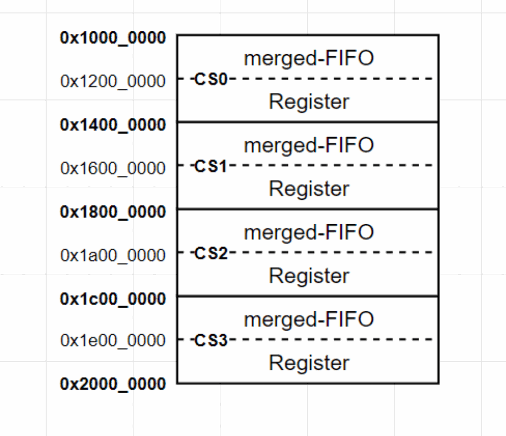
If the slave is Local Bus, the rockchip,ranges property configures the size of the maximum region space. In the case of only enabling the Register and merged-FIFO 2 regions, the region space division for each CS is as follows:
Editable transcription of the figure:
| CS | Region | Start boundary | Next boundary |
|---|---|---|---|
| cs0 | merged-FIFO | 0x10000000 | 0x12000000 |
| cs0 | Register | 0x12000000 | 0x14000000 |
| cs1 | merged-FIFO | 0x14000000 | 0x16000000 |
| cs1 | Register | 0x16000000 | 0x18000000 |
| cs2 | merged-FIFO | 0x18000000 | 0x1a000000 |
| cs2 | Register | 0x1a000000 | 0x1c000000 |
| cs3 | merged-FIFO | 0x1c000000 | 0x1e000000 |
| cs3 | Register | 0x1e000000 | 0x20000000 |
3.3 kernel Configuration
Symbol: ROCKCHIP_DSMC [=y]
       │
  │ Type : bool
       │
  │ Prompt: Rockchip DSMC(Double Data Rate Serial Memory Controller) driver
       │
  │ Depends on: MEMORY [=y]
       │
  │ Location:
       │
  │ -> Device Drivers
       │
  │ -> Memory Controller drivers (MEMORY [=y])
       │
  │ -> Rockchip DSMC(Double Data Rate Serial Memory Controller) driver (ROCKCHIP_DSMC
[=y])│
4. Kernel Mode Access to DSMC
4.1 Driver Interface Invocation
The DSMC driver in drivers/memory/rockchip/dsmc-host.c implements the following access interfaces:
struct rockchip_dsmc_device *rockchip_dsmc_find_dev(void);
static struct dsmc_ops rockchip_dsmc_ops = {
    .read = dsmc_read,
    .write = dsmc_write,
    .copy_from = dsmc_copy_from,
    .copy_from_state = dsmc_copy_from_state,
    .copy_to = dsmc_copy_to,
    .copy_to_state = dsmc_copy_to_state,
};
By calling the function rockchip_dsmc_find_device_by_compat() , the DSMC device is searched for, and the private parameters of this device are obtained. CPU and DMA access to the DSMC slave device is implemented through dsmc_dev.ops . The ops->read and ops->write are used for CPU read and write operations to the DSMC slave device’s memory space. The ops->copy_from is used for DMA to read from the slave device memory and write to the host’s memory. The ops->copy_to is used for DMA to write from the host’s memory to the slave device memory.
static void test(void)
{
    u32 cs;
    struct rockchip_dsmc_device *dsmc_dev;
    dsmc_dev = rockchip_dsmc_find_device_by_compat(rockchip_dsmc_get_compat(0));
    if (dsmc_dev == NULL){
        printk("error: can not find dsmc device\n");
        return 0;
    }
    for (cs = 0; cs < DSMC_MAX_SLAVE_NUM; cs++) {
        if (dsmc_dev->dsmc.cfg.cs_cfg[i].device_type == DSMC_UNKNOWN_DEVICE)
            continue;
        dsmc_dev->ops->write(dsmc_dev, cs, 0, test_addr, test_data);
        /* TODO */
    }
}
4.2 Direct Access
The CPU or master can directly access the DSMC slave memory space (supporting random address access for Byte, half-word, and word; supporting cacheable, uncacheable, and write-combine mapping methods).
5. User Mode Access to DSMC
5.1 Access through Specific Nodes
In the case of Local Bus enabled, the DSMC driver will create 4 slave device chip select (CS) nodes under /dev/dsmc/ , and under each CS, 4 memory regions will be created, with each attribute corresponding to the descriptions in the DTS. If there is a need to access the merged-FIFO, it corresponds to region0, and the corresponding region node under the respective CS needs to be operated. The process is as follows:
1. Use the open() interface to open the corresponding region device node and obtain the file descriptor.
2. Use the mmap() system call to map the aforementioned region device memory into the process address space and obtain the mapped address.
3. Read and write device memory.
4. Use munmap() to unmap the memory.
5. Use close() to close the file descriptor.
The code example is as follows:
device_name = "/dev/dsmc/cs0/region0"
wantbytes = 0x200000;
memfd = open(device_name, O_RDWR | O_SYNC);
if (memfd == -1) {
    fprintf(stderr, "failed to open %s for physical memory: %s\n",
        device_name, strerror(errno));
    exit(EXIT_FAILURE);
}
/*
 * Open the file with O_SYNC flag and MAP_LOCKED flag to make the
 * memory space uncached for mmap operation.
 */
buf = (void volatile *) mmap(0, wantbytes, PROT_READ | PROT_WRITE,
                                 MAP_SHARED | MAP_LOCKED, memfd,
                                 0x0);
if (buf == MAP_FAILED) {
        fprintf(stderr, "failed to mmap %s for physical memory: %s\n",
                device_name, strerror(errno));
        exit(EXIT_FAILURE);
}
bufsize = wantbytes;
halflen = bufsize / 2;
count = halflen / sizeof(u32);
bufa = (u32v *) buf;
bufb = (u32v *) ((size_t) buf + halflen);
test_dsmc(bufa, bufb, count);/* Read or write DSMC slave memory */
if (munmap((void*)buf, wantbytes) == -1) {
    perror("munmap");
    close(memfd);
    exit(EXIT_FAILURE);
}
close(memfd);
5.2 Direct Access
The CPU can directly access the DSMC slave memory space mapped by dev/mem . For example, on RK3576, use the io command to access region0 of the DSMC slave memory: io -4 0x10000000 .
6. DSMC Slave Memory Allocation
The allocation of memory space for DSMC slaves is controlled by the rockchip,ranges attribute, which configure the starting address and size of the device’s memory space.
6.1 PSRAM
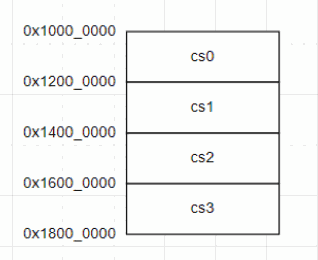
For example, if configuring map, ranges = <0x0 0x10000000 0x0 0x2000000>; and the slave is PSRAM, the map, ranges configuration represents the size of the maximum CS (Chip Select) space. For the DSMC controller, each slave has the same capacity. If different slaves are populated with PSRAM of different capacities, it is important to pay attention to the boundaries when accessing them. The memory space allocation for each slave is as follows:
Editable transcription of the figure:
| CS | Start boundary | Next boundary |
|---|---|---|
| cs0 | 0x10000000 | 0x12000000 |
| cs1 | 0x12000000 | 0x14000000 |
| cs2 | 0x14000000 | 0x16000000 |
| cs3 | 0x16000000 | 0x18000000 |
Note: In theory, DSMC supports different slave with PSRAM from different manufacturers, allowing for different capacities. However, the bit width (x8 or x16) of different slave must be the same.
6.2 Local bus
If the slave is the Local Bus, each slave has the same capacity for the DSMC controller as well. Each slave can be divided into 1, 2, or 4 regions, with each region having attributes such as DPRAM, Register, merged FIFO, and un-merged FIFO. If the actual capacities of the regions in each slave are different, attention should be paid to the boundaries when accessing them.
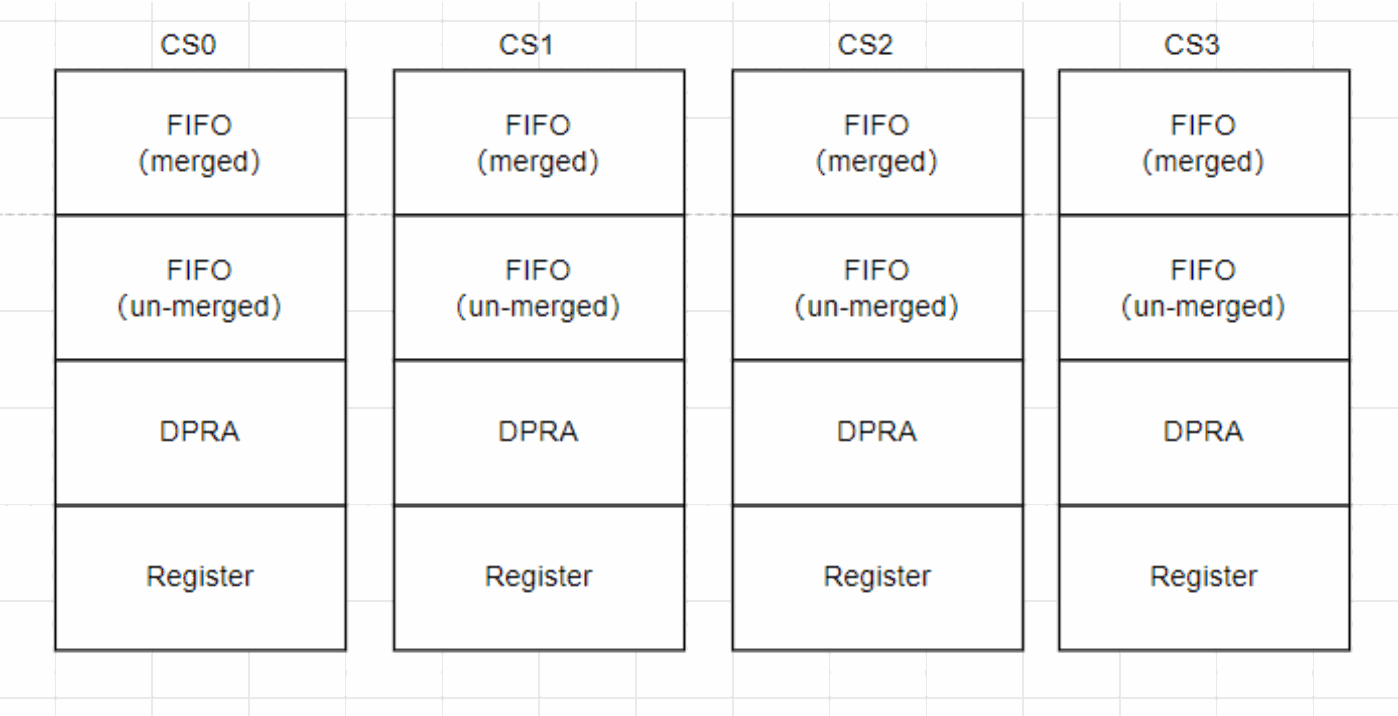
Editable transcription of the figure:
| Region | CS0 | CS1 | CS2 | CS3 |
|---|---|---|---|---|
| 0 | FIFO (merged) | FIFO (merged) | FIFO (merged) | FIFO (merged) |
| 1 | FIFO (un-merged) | FIFO (un-merged) | FIFO (un-merged) | FIFO (un-merged) |
| 2 | DPRA | DPRA | DPRA | DPRA |
| 3 | Register | Register | Register | Register |
For the Local Bus, the map, ranges configuration represents the size of the maximum region space.
If the slave has 2 regions enabled, the size of each region is determined by the DTS (Device Tree Source) with map, ranges = 0x0 0x10000000 0x0 0x2000000 for the DSMC node of the slave device. The memory space allocation for each region in each CS is as follows:
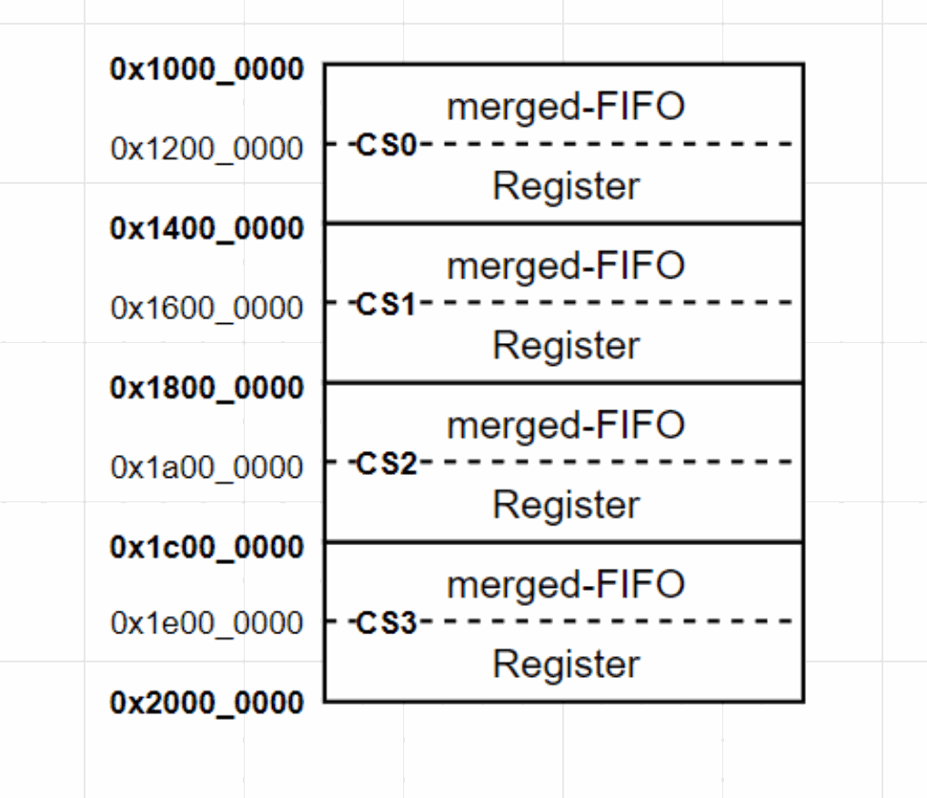
Editable transcription of the figure:
| CS | Region | Start boundary | Next boundary |
|---|---|---|---|
| cs0 | merged-FIFO | 0x10000000 | 0x12000000 |
| cs0 | Register | 0x12000000 | 0x14000000 |
| cs1 | merged-FIFO | 0x14000000 | 0x16000000 |
| cs1 | Register | 0x16000000 | 0x18000000 |
| cs2 | merged-FIFO | 0x18000000 | 0x1a000000 |
| cs2 | Register | 0x1a000000 | 0x1c000000 |
| cs3 | merged-FIFO | 0x1c000000 | 0x1e000000 |
| cs3 | Register | 0x1e000000 | 0x20000000 |
7. DSMC Local bus data interaction between the host and slave
7.1 FIFO
When the DSMC uses the Local bus protocol and is connected to an rockchips designed slave, the slave has a FIFO. When accessing a region with the attributes “merged-FIFO” or “un-merged FIFO”, the data transmitted from the host passes through the FIFO and is then written into the slave’s memory, such as DDR or SRAM. This FIFO is not visible, and for the DSMC host, the memory space of the slave’s DDR or SRAM is considered the slave’s memory space. Any data written through DSMC will ultimately be written into the slave’s memory. It is important to manage the slave’s memory space and ensure data consistency when using it.
7.2 Register
When the DSMC uses the Local bus protocol and is connected to an rockchips designed slave, there is a register called “SLAVE_CSR Register”. When accessing a region with the attribute “Register”, it refers to accessing this segment of the SLAVE_CSR Register. This segment can be used for fast information exchange between the host and slave.
The registers available for information exchange:
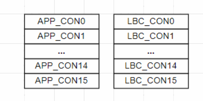
Editable transcription of the figure:
| APP_CONx | LBC_CONx |
|---|---|
| APP_CON0 | LBC_CON0 |
| APP_CON1 | LBC_CON1 |
| … | … |
| APP_CON14 | LBC_CON14 |
| APP_CON15 | LBC_CON15 |
Among them, the APP_CONx registers have read and write permissions for the slave, while the host only has read permissions. The LBC_CONx registers have read permissions for the slave, while the host has read and write permissions.
When the host writes to the LBC_CONx registers, it triggers a host2slave interrupt to the slave’s CPU, which is used to process the data transmitted from the host.
When the slave writes to the APP_CONx registers, it triggers a slave2host interrupt through the INT pin, which is then received by the host. The host’s CPU can also respond to the interrupt and retrieve the data passed from the slave. After receiving the INT signal, DSMC can also initiate a DMA hardware request to start data transfer (DMA needs to be configured in advance).
Typical Scenario 1
The host writes information to the LBC_CONx registers, triggering a host2slave interrupt. The slave reads the information from the LBC_CONx registers. The slave writes information to the APP_CONx registers, triggering a slave2host interrupt. The host reads the information from the APP_CONx registers.
Typical Scenario 2
After the DSMC and DMA on the host side are configured, the host notifies the slave by writing to the LBC_CONx registers. The slave then writes to the APP_CONx registers to return a valid signal to the host through the INT pin. After receiving this signal, DSMC host initiates a DMA hardware request to start the data transfer.
Note: APP_CON15 and LBC_CON15 are already in use. The DSMC driver for DMA hardware request has been implemented. When the host’s DMA configuration is completed, the host writes the original value of LBC_CON15 plus 1 to the LBC_CON15 register. The slave, upon receiving this data, writes 1 to the APP_CON15 register to trigger a slave2host interrupt. DSMC host automatically initiates a certain number of DMA hardware requests upon receiving this interrupt, initiating the data transfer.
8. Note
8.1 Interface Frequency on DSMC IO
1. It is configured by the parameter clock-frequency = <100000000>; in the dsmc node of the dts. However, the actual frequency may not exactly match the target frequency due to dependencies on the PLL or crystal oscillator output of the current platform. The final frequency will be set to the closest achievable value.
2. The DSMC controller has an inherent fixed 2-divider, meaning the frequency provided by the PLL or crystal oscillator to the DSMC controller is twice the frequency on the DSMC IO interface.
8.2 Regarding DSMC Bit Width
1. The bit width of an externally connected DSMC slave cannot be auto-detected. By default, the code assumes a x16 bit width. If an RK3506 is connected as a DSMC slave (which only supports x8 bit width), the bit width must be manually corrected.
In the new version, the io-width of the slave can be modified in the dts.
&dsmc_slave {
    status = "okay";
    lb-slave {
        rockchip,io-width = <8>;
        ...
    };
};
For the old version, it needs to be modified in the code.
diff --git a/drivers/memory/rockchip/dsmc-host.c b/drivers/memory/rockchip/dsmc-host.c
index 44182923acc9..5214c9128320 100644
--- a/drivers/memory/rockchip/dsmc-host.c
+++ b/drivers/memory/rockchip/dsmc-host.c
@@ -782,7 +782,7 @@ static void dsmc_data_init(struct rockchip_dsmc *dsmc)
                        cs_cfg->rd_bdr_xfer_en = 1;
                        cs_cfg->wr_bdr_xfer_en = 1;
                } else {
- cs_cfg->io_width = MCR_IOWIDTH_X16;
+ cs_cfg->io_width = MCR_IOWIDTH_X8;
                        cs_cfg->wrap_size = DSMC_BURST_WRAPSIZE_16CLK;
                        cs_cfg->wrap2incr_en = 1;
                        cs_cfg->acs = 1;
2. If connected to PSRAM, the bit width is auto-detected and does not require manual modification. If the PSRAM supports both x8 and x16 modes, the x16 mode is used by default.
8.3 System Boot Failure After Enabling DSMC
After DSMC is enabled, it attempts to read/write from/to the slave. If an access error occurs (e.g., no DQS signal returned during read), DSMC reports an error to the bus, causing the system to enter an exception state. A typical error log is as follows:
...
[ 1.391589] dsmc 21ca0000.dsmc: init cs0 LB device # After being loaded, the DSMC driver
will access the slave.
[ 1.394238] 8<--- cut here ---
[ 1.394243] Unhandled fault: external abort on non-linefetch (0x1008) at 0xf0600100
[ 1.394250] [f0600100] *pgd=40b0f811, *pte=10000653, *ppte=10000453
[ 1.394267] Internal error: Oops - BUG: 1008 [#1] PREEMPT SMP THUMB2
...
If this issue occurs, check the hardware connectivity between the DSMC master and slave.
Note: During DSMC master initialization, the slave must already be powered on and initialized; otherwise, access exceptions may occur.
8.4 DSMC Self-Test Status Abnormal
After the DSMC driver initialization is completed, it checks the DSMC status registers to confirm whether any abnormalities occurred during initialization. When the following abnormal messages appear, it indicates that there was an exception during initialization.
dsmc ff8b0000.dsmc: DSMC: csr status error(0x800)! #The specific status error value may vary
dsmc ff8b0000.dsmc: DSMC status error, please check hardware matched(io, slave etc.)
If this issue occurs, check the hardware connectivity between the DSMC master and slave.
Note: During DSMC master initialization, the slave must already be powered on and initialized; otherwise, access exceptions may occur.