
This is a Rockchip eDP platform reference. The source product table lists RK3288/RK3399 with Linux kernel 4.4 or later, RK356x with 4.19 or later, RK3588 with 5.10 or later, and RK3576 with 6.1 or later. For an ArmSoM project, verify the actual board SoC, exposed eDP interface, panel power/backlight, HPD/PHY wiring, SDK/BSP and kernel patches. SoC capabilities do not establish support on every board. No ArmSoM hardware validation was performed; the 470mW PSR figure, logs and display photos are source examples, not ArmSoM measurements.
Source: Rockchip eDP Interface Developer Guide, V2.3.0 in both languages. Chinese follows the Chinese source; English and Russian follow the English source, retaining the same technical chapters. Chinese figures come from the Chinese PDF; English and Russian figures come from the English PDF. Source inconsistencies, including the RK3399 rate table versus the bandwidth example, are recorded without silently changing addresses or configuration constants.
Editorial notes · ArmSoM documentation · Rockchip
1. Overview
This document primarily introduces the basic features, workflow, and analysis guide for common issues related to the eDP display interface of Rockchip platform processors. The purpose is to enable engineers to have a better understanding of the eDP interface display driver framework and hardware interface of the Rockchip platform, and to quickly locate, optimize, and resolve issues through the analysis of common problems.
2. eDP Basic Introduction
2.1 DRM Display Framework
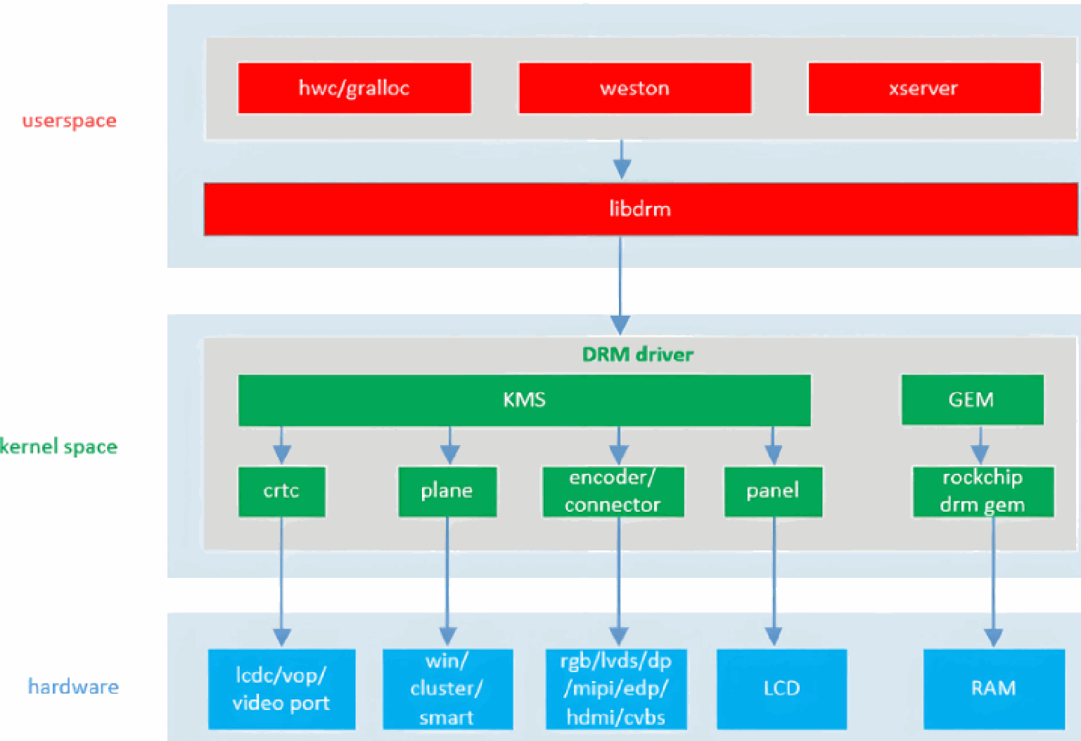
The interaction process between applications and the DRM driver through libdrm is as follows:
2.2 eDP Interface System Framework
The following figure is a typical application block diagram of eDP:
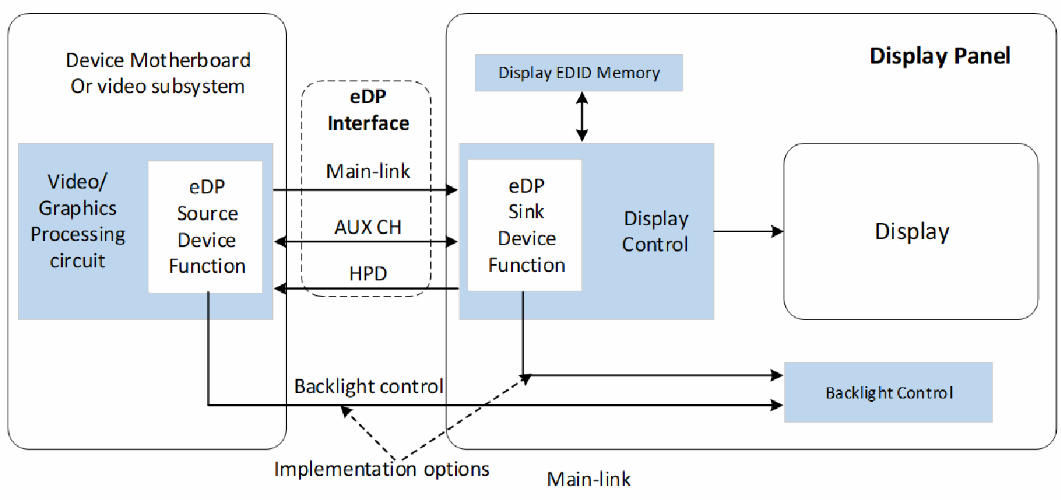
The eDP protocol is an expansion of the DP (Display Port) protocol in the direction of embedded applications and has been widely used in product fields such as laptops, tablet computers, and mobile phones.
The eDP hardware interface mainly consists of Main-Link, AUX CH, and HPD, which together achieve the interactive functions between eDP Source and Sink devices.
Main-Link: Composed of 1/2/4 pairs of differential signals, used for transmitting video and audio data streams
eDP v1.3 supports RBR 1.62G/HBR 2.7G/HBR2 5.4G bps/lane, while eDP v1.4 adds R216 2.16G/R243 2.43G/R324 3.24G/R432 4.32G bps/lane four recommended rates.
AUX CH: A pair of half-duplex differential data transmission paths, used for the exchange of configuration information between Source and Sink devices, such as DPCD reading and writing and EDID parsing, with a transmission rate of 1 Mbps.
HPD: At the Source end, it is usually a single pin with hot-plug detection functionality, used to detect the connection status of the Sink device and respond to its HDP IRQ requests.
When the Sink device changes from the disconnected state to the connected state, the HPD pin should change from low to high level.
HPD can reflect the working status of the Sink device. When HPD is high, it usually indicates that the Sink is in a ready state for normal display. It is recommended to connect the HPD pins at both ends of the Source and Sink during the hardware design phase.
2.3 eDP Link Training
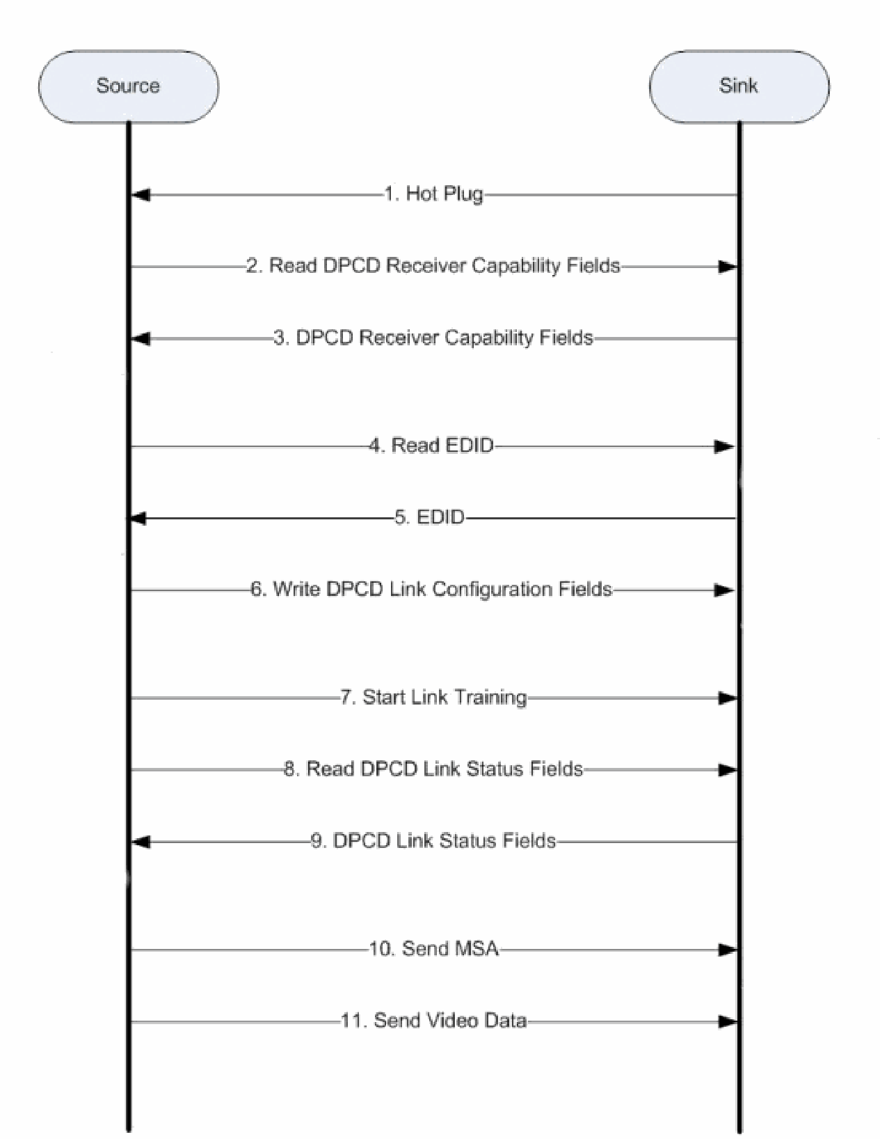
As shown in the figure above, the process of Link Training is as follows:
1: After the Sink is powered on, it sends an HPD Plug pulse signal to the Source;
2-3: The Source reads the Sink DPCD to determine the supported Features of the Sink;
4-5: The Source reads the Sink EDID to determine the display timing information supported by the Sink;
6: The Source writes the Link configuration into the DPCD, such as the typical MAX_LINK_RATE and MAX_LANE_COUNT;
7: The Source initiates Link Training, and the Sink performs Clock Recovery and Equalization;
8-9: The Source reads the DPCD to obtain the Link Status to determine the result of the Link Training. If it fails, it retreats to step 7;
10: After the Link Training is successful, the Source sends MSA data, and the Sink parses the video stream configuration and recovers the Stream Clock;
11: The Source transmits the video data stream.
3. Introduction to Rockchip Platform eDP
3.1 Feature Highlights
| Feature | RK3288 | RK3399 | RK3568 | RK3588 | RK3576 |
|---|---|---|---|---|---|
| eDP Version | v1.3 | v1.3 | v1.3 | v1.3 | v1.3 |
| DP Mode | Not supported | Not supported | Not supported | v1.2 | v1.2 |
| Max Resolution | 2560x1600@60Hz | 2560x1600@60Hz | 2560x1600@60Hz | 3840x2160@60Hz | 3840x2160@60Hz |
| Main-Link Lanes | 1/2/4 lanes | 1/2/4 lanes | 1/2/4 lanes | 1/2/4 lanes | 1/2/4 lanes |
| Main-Link Rate | 2.7/1.62 Gbps/lane | 2.7/1.62 Gbps/lane | 2.7/1.62 Gbps/lane | 5.4/4.32/3.24/2.7/2.43/2.16/1.62 Gbps/lane | 5.4/4.32/3.24/2.7/2.43/2.16/1.62 Gbps/lane |
| AUX_CH | 1 M | 1 M | 1 M | 1 M | 1 M |
| Color Format | RGB | RGB | RGB | RGB/YUV444/YUV422 | RGB/YUV444/YUV422 |
| Color Depth | 8 bpc | 8 bpc | 8 bpc | 8/10 bpc (6bpc just for RGB) | 8/10 bit (6bpc just for RGB) |
| ASSR | Supported | Supported | Supported | Supported | Supported |
| I2S | Not supported | Not supported | Not supported | Supported | Supported |
| SPDIF | Not supported | Not supported | Not supported | Supported | Supported |
| PSR | Not supported | Not supported | Not supported | Supported | Supported |
| Display Split Mode | Not supported | Not supported | Not supported | Supported | Supported |
3.2 eDP Connection with VOP
For detailed information, refer to the document “Rockchip_Developer_Guide_DRM_Display_Driver_CN” in the section “VOP2 Platform Display Pathway”.
3.3 Driver Files
U-Boot Drivers:
/* Controller */
drivers/video/drm/analogix_dp.c
drivers/video/drm/analogix_dp.h

drivers/video/drm/analogix_dp_reg.c

/* PHY */
/* RK3568 */
drivers/phy/phy-rockchip-naneng-edp.c
/* RK3588/RK3576 */
drivers/phy/phy-rockchip-samsung-hdptx.c

/* Panel */
drivers/video/drm/rockchip_panel.c
Kernel Drivers:
/* Controller */
drivers/gpu/drm/bridge/analogix/analogix_dp_core.c

drivers/gpu/drm/bridge/analogix/analogix_dp_core.h
drivers/gpu/drm/bridge/analogix/analogix_dp_reg.c
drivers/gpu/drm/bridge/analogix/analogix_dp_reg.h
drivers/gpu/drm/rockchip/analogix_dp-rockchip.c
include/drm/bridge/analogix_dp.h

/* PHY */
/* RK3568 */
drivers/phy/rockchip/phy-rockchip-naneng-edp.c
/* RK3588/RK3576 */
drivers/phy/rockchip/phy-rockchip-samsung-hdptx.c

/* Panel */

drivers/gpu/drm/panel/panel-simple.c
For RK3288/RK3399 eDP PHY, there is no separate driver; the Analogix DP Controller driver includes PHY-related configuration operations.
4. Software Configuration
4.1 Module Enable
4.1.1 Controller DTS Configuration
The DTS configuration for the eDP controller depends on the type of connected display device, distinguishing between Panel (screen) and Monitor (display) scenarios. The following text will use the eDP0 output on the RK3588 platform as an example for illustration.
4.1.1.1 HPD Configuration
Although the eDP protocol specifies HPD functionality as Optional, the level of HPD is an important basis for determining the working status of the Sink device, and it is recommended to consider the configuration of HPD functionality during the hardware design phase.
If there is an anomaly at the screen end, HPD can notify the master control to avoid problems.
Configuring HPD can effectively reduce display anomalies caused by unreasonable timing configuration, such as AUX errors and Link Training failures.
If the hardware design does not support HDP functionality, Force HPD configuration must be enabled; for designs that require HDP, the Rockchip platform can support both Function Pin HPD and GPIO HPD methods:
Force HPD
&edp0 {
 force-hpd;
};
Function Pin HPD:
&edp0 {
 pinctrl-names = "default";
 pinctrl-0 = <&hdmim0_tx0_hpd>;

};
The HPD Function Pin pinctrl configurations for various platforms are as follows, and should be confirmed according to the specific hardware design schematic.
| Pinctrl Configuration | |
|---|---|
| RK3288 | edp_hpd (GPIO7_B3) |
| RK3399 | edp_hpd (GPIO4_C7) |
| RK3568 | edpdpm0_pins (GPIO4_C4) | edpdpm1_pins (GPIO0_C2) |
| RK3588 | hdmim0_tx0_hpd (GPIO1_A5) | hdmim0_tx1_hpd (GPIO1_A6) | hdmim1_tx0_hpd (GPIO3_D4) | hdmim1_tx1_hpd (GPIO3_B7) |
| RK3576 | edp_txm0_pins (GPIO4_C1) | edp_txm1_pins (GPIO0_B6) |
GPIO HPD:
Any GPIO can be chosen to implement the HPD function.
&edp0 {
 pinctrl-names = "default";
 pinctrl-0 = <&edp0_hpd>;

 hpd-gpios = <&gpio1 RK_PA5 GPIO_ACTIVE_HIGH>;
};

&pinctrl {
 edp {
   edp0_hpd: edp0-hpd {
    rockchip,pins = <1 RK_PA5 0 &pcfg_pull_none>;
   };
 };
};
If there is an anomaly where the driver misidentifies the state as Connected when the Source and Sink devices are not connected by a cable, the corresponding GPIO can be configured as a pull-down to improve stability.
&pinctrl {
 edp {
   edp0_hpd: edp0-hpd {

    rockchip,pins = <1 RK_PA5 0 &pcfg_pull_down>;
   };
 };
};
4.1.1.2 Panel Scenario
&edp0 {
   status = "okay";
   pinctrl-names = "default";

   pinctrl-0 = <&hdmim0_tx0_hpd>;

   ports {
      port@1 {
         reg = <1>;

         edp_out_panel: endpoint {
           remote-endpoint = <&panel_in_edp>;
         };
      };
   };
};
4.1.1.3 Monitor Scenario
The eDP interface of the RK3588/RK3576 platform can support DP mode. When used as DP, it is necessary to configure HPD (see 《HPD DTS Configuration》).
Refer to DTS arch/arm64/boot/dts/rockchip/rk3588-evb1-lp4-v10-hdmi2dp.dts (naming reason: Since HDMI and eDP PHY are combo, this board directly converts the HDMI socket into a DP socket to use eDP as DP):
&edp1 {
   pinctrl-names = "default";
   pinctrl-0 = <&hdmim0_tx1_hpd>;

   status = "okay";
};
4.1.2 PHY DTS Configuration
For RK3568/RK3588/RK3576, PHY DTS configuration is required, whereas RK3288/RK3399 does not need it.
/* RK3568 */
&edp_phy {
      status = "okay";

};

/* RK3588/RK3576 */
&hdptxphy0 {
     status = "okay";
};

&hdptxphy_hdmi0 {
     status = "disabled";
};
On RK3588 and RK3576, the eDP and HDMI interfaces are Combo on the PHY. When using eDP, ensure that the corresponding HDMI PHY nodes hdptxphy_hdmi0/hdptxphy_hdmi1 are disabled.
On RK3588 and RK3576, the eDP PHY can support the configuration of Link Training Table to replace default values, used for optimizing signal quality and adjusting eye diagram indicators, etc.
&hdptxphy0 {
      /* Single Vdiff Training Table (optional) */
      training-table = /bits/ 8 <

         /* voltage swing 0, pre-emphasis 0->3 */
         0x0d 0x0a 0x04 0x06 0x00 0x04
         0x0d 0x0a 0x04 0x06 0x00 0x04
         0x0d 0x0a 0x04 0x06 0x00 0x04
         0x0d 0x0a 0x04 0x06 0x00 0x04
         /* voltage swing 1, pre-emphasis 0->2 */
         0x0d 0x0a 0x04 0x06 0x00 0x04
         0x0d 0x0a 0x04 0x06 0x00 0x04
         0x0d 0x0a 0x04 0x06 0x00 0x04
         /* voltage swing 2, pre-emphasis 0->1 */
         0x0d 0x0a 0x04 0x06 0x00 0x04
         0x0d 0x0a 0x04 0x06 0x00 0x04

         /* voltage swing 3, pre-emphasis 0 */
         0x0d 0x0a 0x04 0x06 0x00 0x04
      >;
      status = "okay";
};
RK3588 and RK3576 eDP support Lane differential signal P/N Swap functionality, which can be used in hardware design scenarios where the Lane P/N signals between Source and Sink are reversed. The reference configuration is as follows:
&hdptxphy0 {
      /* swap lane1 P/N */

      lane-polarity-invert = <0 1 0 0>;
      status = "okay";
};
4.1.3 Panel DTS Configuration
In the Panel scenario, the display timing for eDP is transmitted through the Panel driver. The driver used for eDP Panel on the Rockchip platform is drivers/gpu/drm/panel/panel-simple.c.
For Kernel-5.10 and above, refer to the documentation at Documentation/devicetree/bindings/display/panel/panel-simple.yaml.
For Kernel-4.19 and below, refer to the documentation at Documentation/devicetree/bindings/display/panel/simple-panel.txt.
eDP requires the output of Panel Timing to display normally. For Timing-related information, refer to the “Scan Timing Description” section in the document “Rockchip_Developer_Guide_DRM_Display_Driver_CN.pdf”.
Methods to obtain Panel Timing include:
Obtaining through reading EDID (recommended method)
Obtaining from the Signal Timing Specifications table in the Panel Datasheet
Contacting the screen manufacturer to obtain Panel Timing
Note: For some screens, the EDID may be damaged and unreadable. In such cases, it is suggested to obtain Timing from other methods.
There are two ways to configure DTS:
Not configuring the Timing node, obtaining Timing through EDID and outputting (recommended configuration)
Configuring the Timing node, outputting through the fixed Timing configured
HPD and Delay Requirements:
If using the method without configuring the Timing node, it is necessary to connect HPD in the hardware design to prevent issues caused by timing abnormalities
For the method of configuring the Timing node, it is also recommended to connect HPD
If HPD is not connected, it is necessary to configure prepare-delay-ms (controls the interval from VCC power-on to the first AUX access) to meet the Panel power-on timing requirements.
4.1.3.1 Configuring with EDID DTS
Taking the RK3588S EVB1 as an example, the corresponding DTS for Kernel-6.1 is located at arch/arm64/boot/dts/rockchip/rk3588s-evb1-lp4x.dtsi.
panel-edp {
   compatible = "simple-panel";
   backlight = <&backlight>;

   power-supply = <&vcc3v3_lcd_edp>;
   prepare-delay-ms = <120>;
   enable-delay-ms = <120>;
   unprepare-delay-ms = <120>;
   disable-delay-ms = <120>;
   width-mm = <120>;
   height-mm = <160>;

   port {
      panel_in_edp: endpoint {
         remote-endpoint = <&edp_out_panel>;
      };
   };

};
The configuration of pwms for the backlight node needs to be modified according to the actual hardware connections, ensuring that the backlight is properly illuminated before displaying images.
For details, refer to the PWM module reference document Rockchip_Developer_Guide_Linux_PWM_CN.
The power-supply configuration is for the panel’s power supply.
For scenarios where the Sink is abnormal, forcibly powering the Panel or Bridge on and off to reset the device is a common method. Ensure that the panel’s power supply can be controlled by the main controller for powering on and off.
enable-gpios/reset-gpios is used for the configuration of the Panel’s enable/reset pins, which need to be modified according to the actual hardware circuit design.
(Optional) The enable pin is typically used for enabling the screen-side power supply, and the gpio configuration depends on the specific design of the power supply circuit.
(Optional) The reset pin is usually directly drawn out from the screen side and the conditions for triggering the reset function are specified in the datasheet. The gpio configuration depends on the specific design of the reset circuit.
The delay-ms configuration must meet the timing requirements for power on/off and reset as specified in the Panel Datasheet.
(Optional) enable-delay-ms/disable-delay-ms is used for delay control after enabling or before disabling the enable pin.
(Optional) reset-delay-ms is used for delay control after enabling the reset pin.
(Optional) prepare-delay-ms/unprepare-delay-ms is used for delay control after powering on or before powering off the power-supply.
(The following explanation about delay-ms is excerpted from Documentation/devicetree/bindings/display/panel/panel-simple.yaml)
......
 prepare-delay-ms:
   description: |

    the time (in milliseconds) that it takes for the panel to
    become ready and start receiving video data
 enable-delay-ms:
   description: |
    the time (in milliseconds) that it takes for the panel to
    display the first valid frame after starting to receive
    video data
 disable-delay-ms:
   description: |
    the time (in milliseconds) that it takes for the panel to
    turn the display off (no content is visible)
 unprepare-delay-ms:

   description: |
    the time (in milliseconds) that it takes for the panel
    to power itself down completely
 reset-delay-ms:
   description: |
    the time (in milliseconds) that it takes for the panel to
    reset itself completely
 init-delay-ms:
   description: |
    the time (in milliseconds) that it takes for the panel to
    send init command sequence after reset deassert
......
4.1.3.2 Fixed Timing DTS Configuration
Advantages of DTS Fixed Panel Timing:
Interfaces no longer read EDID information, avoiding exceptions caused by errors in reading EDID.
Timing parameters can be adjusted according to requirements, avoiding issues where Pixel alignment or Clock special frequency division is needed.
Disadvantages of DTS Fixed Panel Timing:
If the Timing configuration does not meet the Panel requirements, it will cause Training failure or abnormal display.
For special cases of certain Panels, such as disordered EDID data, special Clock frequencies, and the need to adjust Timing parameters, we can fix the Timing DTS configuration.
DRM framework’s description of the display_timing structure and its variables can be found in include/video/display_timing.h, with an example as follows:
/*
 * Single "mode" entry. This describes one set of signal timings a display can
 * have in one setting. This struct can later be converted to struct videomode

 * (see include/video/videomode.h). As each timing_entry can be defined as a
 * range, one struct display_timing may become multiple struct videomodes.
 *
 * Example: hsync active high, vsync active low
 *
 *            Active Video
 * Video ______________________XXXXXXXXXXXXXXXXXXXXXXX____________________
 *  |<- sync ->|<- back ->|<----- active ----->|<- front ->|<- sync..
 *  |    |  porch |        |  porch |
 *
 * HSync _|¯¯¯¯¯¯¯¯¯¯¯|___________________________________________|¯¯¯¯¯¯¯¯¯
 *
 * VSync ¯|__________|¯¯¯¯¯¯¯¯¯¯¯¯¯¯¯¯¯¯¯¯¯¯¯¯¯¯¯¯¯¯¯¯¯¯¯¯¯¯¯¯¯¯¯|_________

 */
struct display_timing {
   struct timing_entry pixelclock;

   struct timing_entry hactive; /* hor. active video */
   struct timing_entry hfront_porch; /* hor. front porch */
   struct timing_entry hback_porch; /* hor. back porch */
   struct timing_entry hsync_len; /* hor. sync len */

   struct timing_entry vactive; /* ver. active video */
   struct timing_entry vfront_porch; /* ver. front porch */
   struct timing_entry vback_porch; /* ver. back porch */

   struct timing_entry vsync_len; /* ver. sync len */

   enum display_flags flags; /* display flags */
};
For the calculation method of Timing basic parameters, refer to the following:
htotal = hsync_len + hback_porch + hactive + hfront_porch
hsync_start = hfront_porch + hactive
hsync_end = htotal - hback_porch = hsync_len + hactive + hfront_porch
vtotal = vsync_len + vback_porch + vactive + vfront_porch
vsync_start = vfront_porch + vactive
vsync_end = vtotal - vback_porch = vsync_len + vactive + vfront_porch
After obtaining Timing, it is configured within the Panel node, and Timing parameters will be recognized and filled into the corresponding display_timing structure by the DRM framework, with the configuration reference as follows:
panel-edp {
   compatible = "simple-panel";
   backlight = <&backlight>;
   power-supply = <&vcc3v3_lcd_edp>;

   prepare-delay-ms = <120>;
   enable-delay-ms = <120>;
   unprepare-delay-ms = <120>;
   disable-delay-ms = <120>;
   width-mm = <120>;
   height-mm = <160>;

   panel-timing {
      clock-frequency = <200000000>;
      hactive = <1536>;
      vactive = <2048>;
      hfront-porch = <12>;

      hsync-len = <16>;
      hback-porch = <48>;
      vfront-porch = <8>;
      vsync-len = <4>;
      vback-porch = <8>;
      hsync-active = <0>;
      vsync-active = <0>;
      de-active = <0>;
      pixelclk-active = <0>;
   };

   port {
      panel_in_edp: endpoint {

         remote-endpoint = <&edp_out_panel>;
      };
   };
};
The clock-frequency property value will determine the frame rate output by VOP, and the calculation requires the DRM framework’s timing attributes htotal and vtotal.
For special cases of clock-frequency that cannot be divided, you can try to zero out the numerical value and retain it to the unit MHz for testing.
The frame rate calculation can refer to the implementation of the drm_mode_vrefresh() function in drivers/gpu/drm/drm_modes.c, with the frame rate denoted as fr, the calculation formula is:
fr = clock / (htotal * vtotal)
/**
 * drm_mode_vrefresh - get the vrefresh of a mode

 * @mode: mode
 *
 * Returns:
 * @modes's vrefresh rate in Hz, rounded to the nearest integer. Calculates the
 * value first if it is not yet set.
 */
int drm_mode_vrefresh(const struct drm_display_mode *mode)
{
   unsigned int num, den;


   if (mode->htotal == 0 || mode->vtotal == 0)
      return 0;

   num = mode->clock;
   den = mode->htotal * mode->vtotal;

   if (mode->flags & DRM_MODE_FLAG_INTERLACE)
      num *= 2;
   if (mode->flags & DRM_MODE_FLAG_DBLSCAN)
      den *= 2;
   if (mode->vscan > 1)
      den *= mode->vscan;


   return DIV_ROUND_CLOSEST_ULL(mul_u32_u32(num, 1000), den);
}
EXPORT_SYMBOL(drm_mode_vrefresh);
The hsync-active/vsync-active/de-active/pixelclk-active properties will determine the polarity of the synchronization signals hsync/vsync/den and pixelclk (macro definitions refer to the display_flags section below)
hsync-active = <0>; Indicates DISPLAY_FLAGS_HSYNC_LOW, meaning the HSYNC signal is low active; otherwise, it is DISPLAY_FLAGS_HSYNC_HIGH, meaning the HSYNC signal is high active.
vsync-active = <0>; Indicates DISPLAY_FLAGS_VSYNC_LOW, meaning the VSYNC signal is low active; otherwise, it is DISPLAY_FLAGS_VSYNC_HIGH, meaning the VSYNC signal is high active.
de-active = <0>;
Indicates DISPLAY_FLAGS_DE_LOW, meaning the DEN signal is low active; otherwise, it is DISPLAY_FLAGS_DE_HIGH, meaning the DEN signal is high active.
pixelclk-active = <0>; Indicates DISPLAY_FLAGS_PIXDATA_NEGEDGE, meaning the DATA signal is valid on the falling edge of Clock; otherwise, it is DISPLAY_FLAGS_PIXDATA_POSEDGE, meaning the DATA signal is valid on the rising edge of Clock.
4.1.3.2.1 Writing Timing Back Through EDID
If there is no Timing node configured in the DTS Panel node (refer to section 4.1.3.1 for an example of using EDID DTS configuration), the default action is to use the AUX channel to read the Panel EDID information.
After connecting the display, the following information will be printed in the U-Boot serial port:
#Old version code prints other EDID information
Maximum visible display size: 26 cm x 17 cm
Power management features: no active off, no suspend, no standby

Established timings:
Standard timings:
2400x1600 59 Hz (detailed)
Monitor name: LQ123P1JX31
Detailed mode clock 252750 kHz, flags[a]
H: 2400 2448 2480 2560
V: 1600 1603 1613 1646
bus_format: 1009
#New version does not print other EDID information
edp@fded0000: detailed mode clock 148500 kHz, flags[5]
   H: 1920 2008 2052 2200

   V: 1080 1084 1089 1125
bus_format: 100a
It is crucial to confirm that the following statement does not appear in the U-Boot Log; if it does, it indicates that the DTS corresponding Panel node is still configured with Timing, and the interface will not read the EDID information:
Using display timing dts
From the above information, we can obtain:
clock-frequency = 252750 kHz
hactive = 2400 hsync_start = 2448 hsync_end = 2480 htotal = 2560
vactive = 1600 vsync_start = 1603 vsync_end = 1613 vtotal = 1646
flags = 0xa
Corresponding to the Timing node’s hsync-active/vsync-active/de-active/pixelclk-active and other display_flags.
The definition of display_flags is detailed in include/video/display_timing.h:
enum display_flags {
   DISPLAY_FLAGS_HSYNC_LOW = BIT(0),
   DISPLAY_FLAGS_HSYNC_HIGH = BIT(1),

   DISPLAY_FLAGS_VSYNC_LOW = BIT(2),
   DISPLAY_FLAGS_VSYNC_HIGH = BIT(3),

   /* data enable flag */
   DISPLAY_FLAGS_DE_LOW = BIT(4),
   DISPLAY_FLAGS_DE_HIGH = BIT(5),
   /* drive data on pos. edge */
   DISPLAY_FLAGS_PIXDATA_POSEDGE = BIT(6),
   /* drive data on neg. edge */
   DISPLAY_FLAGS_PIXDATA_NEGEDGE = BIT(7),
   DISPLAY_FLAGS_INTERLACED = BIT(8),
   DISPLAY_FLAGS_DOUBLESCAN = BIT(9),
   DISPLAY_FLAGS_DOUBLECLK = BIT(10),
   /* drive sync on pos. edge */
   DISPLAY_FLAGS_SYNC_POSEDGE = BIT(11),

   /* drive sync on neg. edge */
   DISPLAY_FLAGS_SYNC_NEGEDGE = BIT(12),
};
bus_format = 1009
Refers to the current color format in use, details are in include/uapi/linux/media-bus-format.h
/* RGB - next is 0x1024 */
#define MEDIA_BUS_FMT_RGB444_1X12 0x1016

#define MEDIA_BUS_FMT_RGB444_2X8_PADHI_BE 0x1001
#define MEDIA_BUS_FMT_RGB444_2X8_PADHI_LE 0x1002
#define MEDIA_BUS_FMT_RGB555_2X8_PADHI_BE 0x1003
#define MEDIA_BUS_FMT_RGB555_2X8_PADHI_LE 0x1004
#define MEDIA_BUS_FMT_RGB565_1X16 0x1017
#define MEDIA_BUS_FMT_BGR565_2X8_BE 0x1005
#define MEDIA_BUS_FMT_BGR565_2X8_LE 0x1006
#define MEDIA_BUS_FMT_RGB565_2X8_BE 0x1007
#define MEDIA_BUS_FMT_RGB565_2X8_LE 0x1008
#define MEDIA_BUS_FMT_RGB666_1X18 0x1009
#define MEDIA_BUS_FMT_RBG888_1X24 0x100e
#define MEDIA_BUS_FMT_RGB666_1X24_CPADHI 0x1015
#define MEDIA_BUS_FMT_RGB666_1X7X3_SPWG 0x1010

#define MEDIA_BUS_FMT_BGR888_1X24 0x1013
#define MEDIA_BUS_FMT_BGR888_3X8 0x101b
#define MEDIA_BUS_FMT_GBR888_1X24 0x1014
#define MEDIA_BUS_FMT_RGB888_1X24 0x100a
#define MEDIA_BUS_FMT_RGB888_2X12_BE 0x100b
#define MEDIA_BUS_FMT_RGB888_2X12_LE 0x100c
#define MEDIA_BUS_FMT_RGB888_3X8 0x101c
#define MEDIA_BUS_FMT_RGB888_3X8_DELTA 0x101d
#define MEDIA_BUS_FMT_RGB888_1X7X4_SPWG 0x1011
#define MEDIA_BUS_FMT_RGB888_1X7X4_JEIDA 0x1012
4.1.3.2.2 Based on Datasheet Calculation
The following figure is excerpted from the example DTS Panel “lg,lp079qx1-sp0v” corresponding Datasheet:
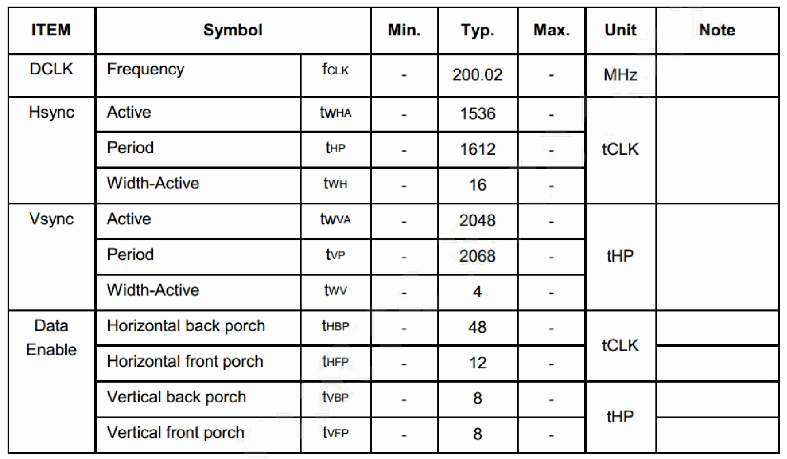
Editable transcription of the timing table above (blank notes remain blank):
| Item | Description | Symbol | Min. | Typ. | Max. | Unit | Note |
|---|---|---|---|---|---|---|---|
| DCLK | Frequency | fCLK | - | 200.02 | - | MHz | |
| Hsync | Active | tWHA | - | 1536 | - | tCLK | |
| Hsync | Period | tHP | - | 1612 | - | tCLK | |
| Hsync | Width-Active | tWH | - | 16 | - | tCLK | |
| Vsync | Active | tWVA | - | 2048 | - | tHP | |
| Vsync | Period | tVP | - | 2068 | - | tHP | |
| Vsync | Width-Active | tWV | - | 4 | - | tHP | |
| Data Enable | Horizontal back porch | tHBP | - | 48 | - | tCLK | |
| Data Enable | Horizontal front porch | tHFP | - | 12 | - | tCLK | |
| Data Enable | Vertical back porch | tVBP | - | 8 | - | tHP | |
| Data Enable | Vertical front porch | tVFP | - | 8 | - | tHP |
According to the Panel Datasheet configuration, users can fine-tune within the upper and lower threshold ranges specified in the Datasheet based on specific application requirements.
Refer to the calculated Timing parameters fixed in the eDP Panel Timing node as mentioned above, and output according to the specified Timing.
4.2 Feature Configuration
4.2.1 Panel Self-Test Mode
This mode is typically used during the Panel debugging phase. If the Panel displays abnormally but shows normal when the Panel Self-Test mode is enabled, it indicates that the Sink end is working properly, and the issue needs to be confirmed from the Source end. For more details, see Common Problems and Analysis Methods.
Taking RK3588S EVB1 arch/arm64/boot/dts/rockchip/rk3588s-evb1-lp4x.dtsi as an example, the DTS needs to add the panel-self-test property to the edp node:
diff --git a/arch/arm64/boot/dts/rockchip/rk3588s-evb1-lp4x.dtsi b/arch/arm64/boot/dts/rockchip/rk3588s-evb1-lp4x.dtsi
index 8c1d0f37b8a3..e58dd8aae2ee 100644

--- a/arch/arm64/boot/dts/rockchip/rk3588s-evb1-lp4x.dtsi
+++ b/arch/arm64/boot/dts/rockchip/rk3588s-evb1-lp4x.dtsi
@@ -262,6 +262,7 @@ &dp0_sound{
 };

 &edp0 {
+     panel-self-test;
      force-hpd;
      status = "okay";
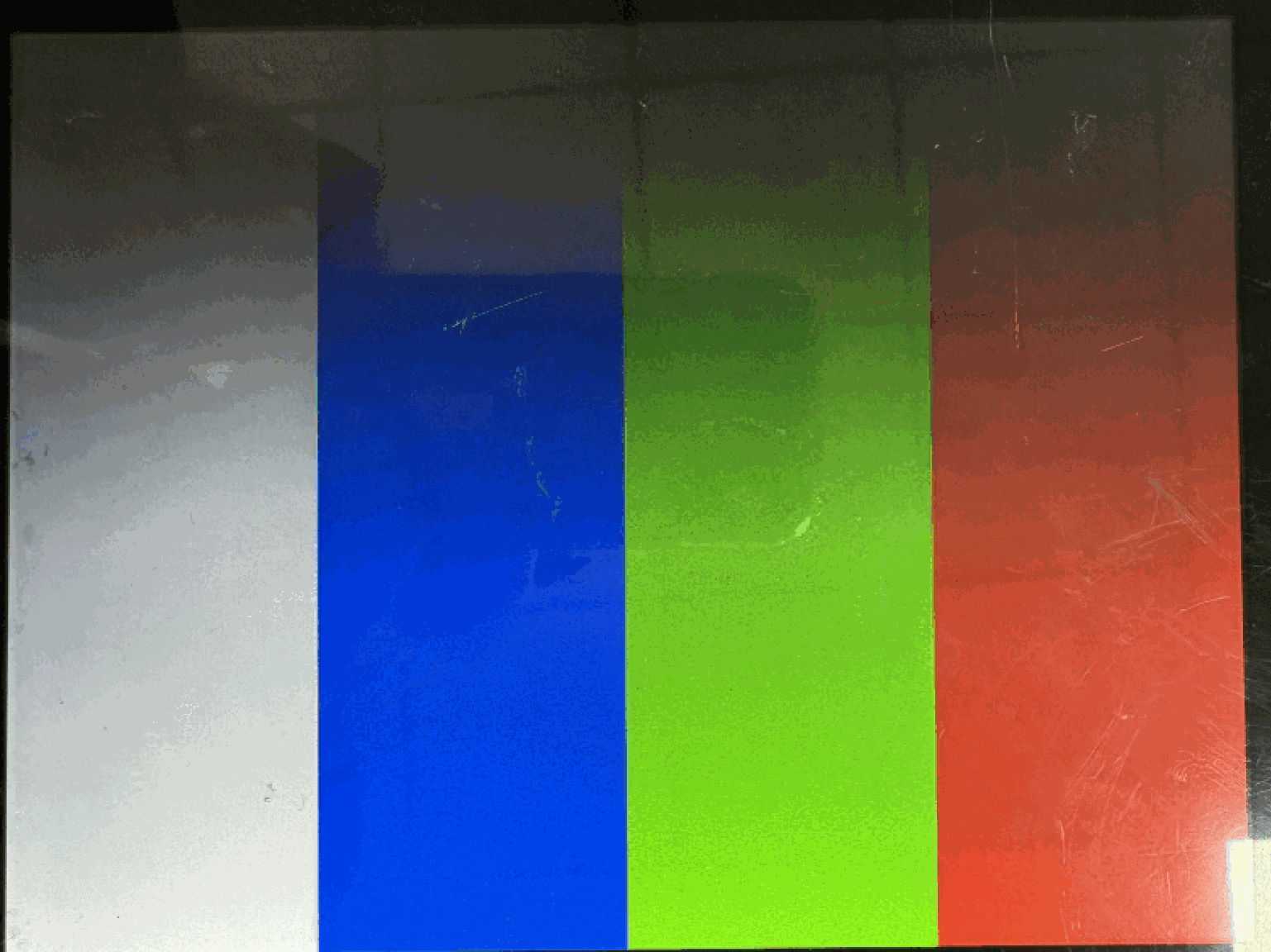
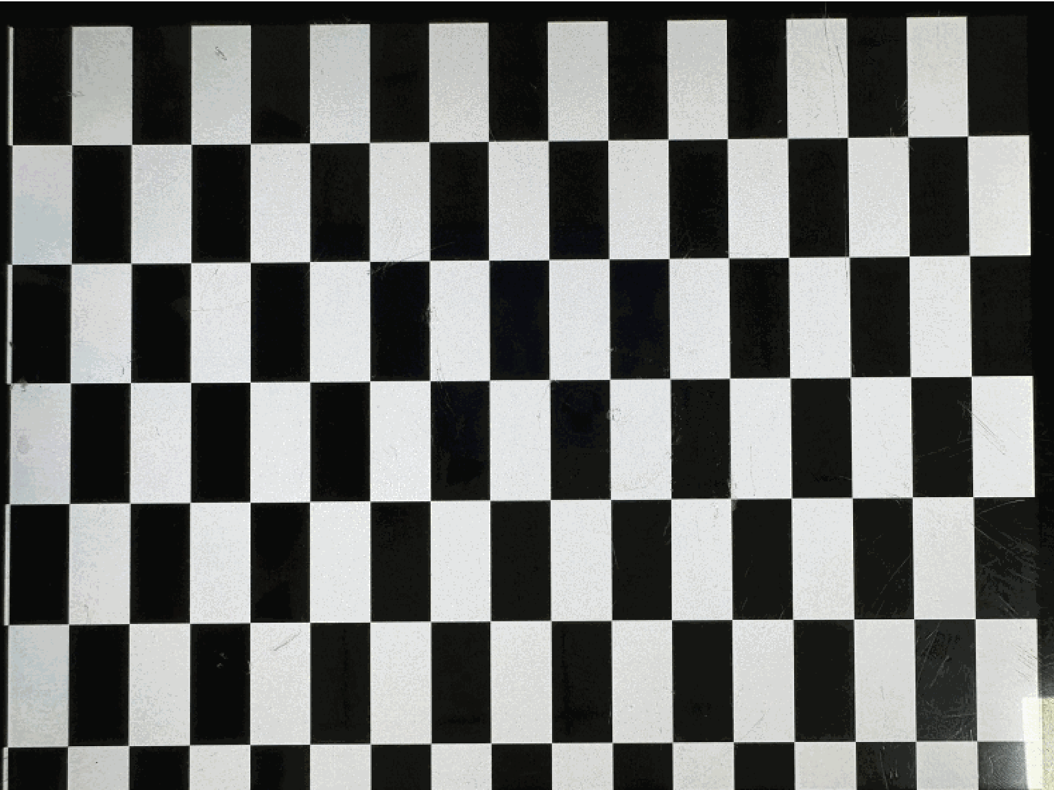
For the “lg,lp079qx1-sp0v” panel, the Panel Self-Test mode is a dynamic switch between the following two images:
4.2.2 Controller Self-Test Mode
This mode is typically used during the panel debugging phase. If a screen displays abnormally but displays normally after enabling the Controller Self-Test mode, it indicates that the display chain from eDP Controller - > PHY -> Panel is normal. The analysis should be conducted upstream of the display chain, specifically on the VOP. For analysis related to VOP, you can refer to the document Rockchip_Developer_Guide_DRM_Display_Driver_CN.
Taking the example of RK3588S EVB1 arch/arm64/boot/dts/rockchip/rk3588s-evb1-lp4x.dtsi, in the DTS, the edp node needs to add the property analogix,video-bist-enable:
diff --git a/arch/arm64/boot/dts/rockchip/rk3588s-evb1-lp4x.dtsi b/arch/arm64/boot/dts/rockchip/rk3588s-evb1-lp4x.dtsi

index 8c1d0f37b8a3..07a9de32f910 100644
--- a/arch/arm64/boot/dts/rockchip/rk3588s-evb1-lp4x.dtsi
+++ b/arch/arm64/boot/dts/rockchip/rk3588s-evb1-lp4x.dtsi
@@ -262,6 +262,7 @@ &dp0_sound{
 };

 &edp0 {
+     analogix,video-bist-enable;
      force-hpd;
      status = "okay";
The eDP Controller Self-Test mode displays the following image by default:

4.2.3 PSR Mode
PSR (Panel Self-Refresh), introduced in eDP v1.3, is an optional feature for both the Source and Sink. It can only be properly enabled when both the Source and Sink ends support this feature.
Once the PSR function is enabled, during static display scenarios (e.g., showing a static Android desktop), both the VOP and eDP modules in the display pipeline (VOP -> eDP -> Panel) will automatically enter a low-power state. This effectively reduces overall system power consumption. Under the Kernel-6.1 DTS configuration arch/arm64/boot/dts/rockchip/rk3576-evb1-v10-edp-NE160QAM-NX1.dts, for a single display connected via eDP -> Panel (NE160QAM-NX1) showing a static desktop, enabling PSR yielded a measured average system power reduction of approximately 470mW.
commit 303b0de1b8fd9f33a8cbfa935e0885c53fe9f78c
Author: Damon Ding <damon.ding@rock-chips.com>

Date: Wed Jul 16 14:22:21 2025 +0800

   drm/bridge: analogix_dp: Add &analogix_dp_plat_data.disable_psr to check whether to
disable PSR

   First of all, since the PSR feature can help to reduce the power
   consumption, the Source device, which can support PSR function,
should enable PSR if the PSR capability of Sink device is detected
rather than depending on the user to add 'support-psr' DTS property
manually.


Different platforms that use the same Analogix DP bridge driver may
have different methods for parsing the PSR capability. Therefore, add
a new flag &analogix_dp_plat_data.disable_psr to disable PSR forcely,
which set in the platform side, should be more reasonable.

If the user truly does not want to enable PSR function or the Panel
has something wrong with it, the property 'rockchip,disable-psr' will
be helpful.

Fixes: 9622f2d0f10a ("drm/bridge: analogix_dp: disable PSR feature by default")
Change-Id: Id2fce34857df80de5a1ec97f342709a6e2840ed4

Signed-off-by: Damon Ding <damon.ding@rock-chips.com>
For the Kernel version that contains the above commit, the eDP interface driver checks the Sink’s PSR support via the DPCD register (DP_PSR_SUPPORTat address 0x70). If the Sink supports the function, the driver will automatically enable the PSR feature on the Source end. If you encounter a situation where the Sink’s DPCD (DP_PSR_SUPPORT) reads as 1(supported) but the PSR function operates abnormally, it is recommended to further confirm the actual PSR support status with the panel manufacturer. As a workaround, you can forcibly disable the PSR function by configuring the rockchip,disable-psrproperty under the edpnode in the device tree.
&edp {
   rockchip,disable-psr;

};
If this commit is not included, you need to manually enable the PSR function by configoring the support-psr property under the edp node:
&edp {
   support-psr;
};
4.2.4 Connector-split Mode
The Connector-split feature provided by VOP2 is a technology similar to MIPI Dual Channel Mode, which allows the output of a single Video Port to be split in half horizontally to drive two timing-consistent identical/different interfaces (for details, see the “Connector-split” section in the document “Rockchip_Developer_Guide_DRM_Display_Driver_CN”).
Taking the dual eDP Connector-split scenario as an example, the application scenarios are as follows:
-
A single VP drives two timing-consistent eDP screens.
-
The two eDP screens display left and right half-screen images, respectively.
-
The DRM framework only registers one Connector, and the application layer can only query the eDP0 device.
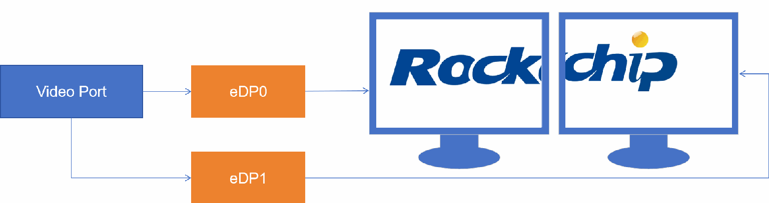
The example DTS configuration is Kernel-6.1 arch/arm64/boot/dts/rockchip/rk3588-vehicle-serdes-display-v20.dtsi, with key configurations as follows:
Both edp0 and edp1 need to be output on the same VP, corresponding to enabling edp0_in_vp1 and edp1_in_vp1 simultaneously in the instance.
The interface displaying on the left in the Connector-split function needs to add the rockchip,split-mode property.
&edp0 {
   rockchip,split-mode;
   force-hpd;

   status = "okay";

   ports {
      port@1 {
         reg = <1>;

         edp0_out_i2c5_bu18tl82: endpoint {
           remote-endpoint = <&i2c5_bu18tl82_in_edp0>;
         };
      };
   };
};


&edp0_in_vp0 {
   status = "disabled";
};

&edp0_in_vp1 {
   status = "okay";
};

&edp0_in_vp2 {
   status = "disabled";
};


&edp1 {
   force-hpd;
   status = "okay";

   ports {
      port@1 {
         reg = <1>;

         edp1_out_i2c7_bu18tl82: endpoint {

           remote-endpoint = <&i2c7_bu18tl82_in_edp1>;
         };
      };
   };
};

&edp1_in_vp0 {
   status = "disabled";
};

&edp1_in_vp1 {
   status = "okay";

};

&edp1_in_vp2 {
   status = "disabled";
};
4.2.5 Dual-channel Mode
The Connector-split function typically maps a single VP-driven interface to two screens/monitors, whereas for scenarios where two identical interfaces drive a single screen/monitor, the rockchip,dual-channel property of the left display interface must be enabled.
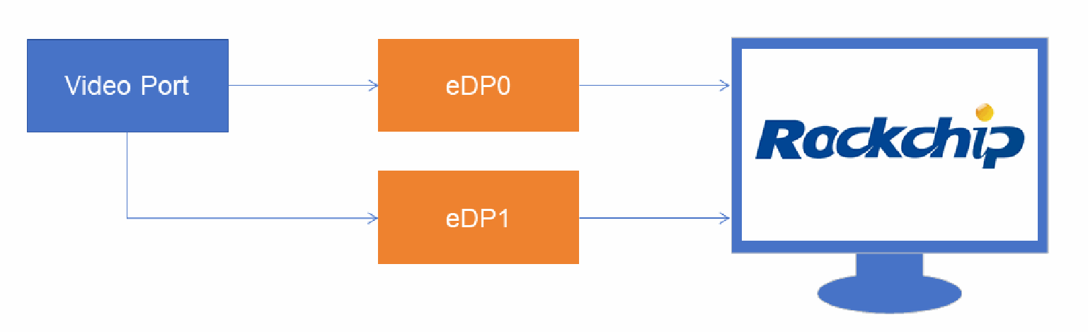
The Dual-channel mode can be understood as a subset of the Connector-split function, sharing the same implementation mechanism. The difference lies in the fact that when the left connector is mapped, the timing must be configured to match the actual output timing of the VP, whereas when the split-mode property is enabled, it is configured to be 1/2 of the actual VP timing.
Taking an 8 lane 3840x2160@144Hz eDP panel module M280DCA as an example, the data mapping required by the datasheet is as follows:
| Area | Lane | Data Stream |
|---|---|---|
| Left | Lane 0 | Pixel 1,5,9, …… ,1913,1917 |
| Lane 1 | Pixel 2,6,10, …… ,1914,1918 | |
| Lane 2 | Pixel 3,7,11, …… ,1915,1919 | |
| Lane 3 | Pixel 4,8,12, …… ,1916,1920 | |
| Right | Lane 4 | Pixel 1921,1925,1929, …… ,3833,3837 |
| Lane 5 | Pixel 1922,1926,1930, …… ,3834,3838 | |
| Lane 6 | Pixel 1923,1927,1931, …… ,3835,3839 | |
| Lane 7 | Pixel 1924,1928,1932, …… ,3836,3840 |
The RK3588 supports a single eDP at 4 lanes for 3840x2160@60Hz, and 8 lanes for 3840x2160@144Hz can be achieved through the Dual-channel function. An example DTS is located at arch/arm64/boot/dts/rockchip/rk3588-evb1-lp4-v10-edp-8lanes-M280DCA.dts, with key configurations as follows:
Both edp0 and edp1 need to output from the same VP, corresponding to enabling both edp0_in_vp0 and edp1_in_vp0 in the example instance.
The rockchip,dual-channel property must be added to the interface of the left display in the Dual- channel function.
/ {
   panel-edp {
      compatible = "simple-panel";

      backlight = <&backlight>;
      power-supply = <&vcc3v3_edp>;
      enable-gpios = <&gpio4 RK_PC1 GPIO_ACTIVE_HIGH>;
      prepare-delay-ms = <120>;
      enable-delay-ms = <120>;
      unprepare-delay-ms = <120>;
      disable-delay-ms = <120>;

      display-timings {
         native-mode = <&timing_4kp144>;
         timing_4kp144: timing0 {
           clock-frequency = <1360800000>;

           hactive = <3840>;
           vactive = <2160>;
           hfront-porch = <160>;
           hsync-len = <40>;
           hback-porch = <160>;
           vfront-porch = <40>;
           vsync-len = <10>;
           vback-porch = <40>;
           hsync-active = <0>;
           vsync-active = <0>;
            de-active = <0>;
            pixelclk-active = <0>;
         };


         timing_4kp120: timing1 {
            clock-frequency = <1188000000>;
            hactive = <3840>;
            vactive = <2160>;
            hfront-porch = <240>;
            hsync-len = <80>;
            hback-porch = <240>;
            vfront-porch = <40>;
            vsync-len = <10>;
            vback-porch = <40>;
            hsync-active = <0>;

            vsync-active = <0>;
            de-active = <0>;
            pixelclk-active = <0>;
         };
      };

      ports {
         #address-cells = <1>;
         #size-cells = <0>;

         port@0 {
            reg = <0>;
            panel_in_edp0: endpoint {

               remote-endpoint = <&edp0_out_panel>;
            };
         };

         port@1 {
            reg = <1>;
            panel_in_edp1: endpoint {
               remote-endpoint = <&edp1_out_panel>;
            };
         };
      };
   };

};

&edp0 {
   force-hpd;
   status = "okay";
   dual-channel;

   ports {
      port@1 {
         reg = <1>;

         edp0_out_panel: endpoint {
            remote-endpoint = <&panel_in_edp>;
         };
      };
   };

};

&edp0 {
   force-hpd;
   rockchip,dual-channel;
   rockchip,data-swap;
   status = "okay";

   ports {
      port@1 {
         reg = <1>;


         edp0_out_panel: endpoint {
            remote-endpoint = <&panel_in_edp0>;
         };
      };
   };
};

&edp0_in_vp0 {
   status = "okay";
};

&edp0_in_vp1 {
   status = "disabled";

};

&edp0_in_vp2 {
   status = "disabled";
};

&edp1 {
   force-hpd;
   status = "okay";

   ports {
      port@1 {

         reg = <1>;

         edp1_out_panel: endpoint {
            remote-endpoint = <&panel_in_edp1>;
         };
      };
   };
};

&edp1_in_vp0 {
   status = "okay";
};
&edp1_in_vp1 {
   status = "disabled";
};


&edp1_in_vp2 {
   status = "disabled";
};
5. Common Debugging Techniques
5.1 Check DRM Connector Status
Taking RK3588S EVB1 as an example, refer to the corresponding DTS file located at arch/arm64/boot/dts/rockchip/rk3588s-evb1-lp4x.dtsi.
Under the Linux system, you can see the registered DRM devices in the /sys/class/drm directory. As shown in the logs below, card0 represents the Display-subsystem device for the Rockchip platform, while card0-DP-1 and card0-eDP-1 correspond to the DP interface device and eDP interface device, respectively.
console:/ # cat /sys/class/drm/
card0-DP-1/   card0-eDP-1/   card1/        renderD129/
card0-Writeback-1/ card0/    renderD128/   version
Taking card0-eDP-1 as an example, its directory contains the following content:
console:/ # ls /sys/class/drm/card0-eDP-1/
device dpms edid enabled modes power status subsystem uevent
dpms: The Power Status of the device.
console:/ # cat /sys/class/drm/card0-eDP-1/dpms
On
edid: The EDID information obtained from the Sink device.
It can be parsed using the edid-decode command:
console:/ # edid-decode /sys/class/drm/card0-eDP-1/edid
edid-decode (hex):


00 ff ff ff ff ff ff 00 16 83 00 00 00 00 00 00
04 17 01 00 a5 10 0c 78 06 ef 05 a3 54 4c 99 26
0f 50 54 00 00 00 01 01 01 01 01 01 01 01 01 01
01 01 01 01 01 01 ea 4e 00 4c 60 00 14 80 0c 10
84 00 78 a0 00 00 00 18 00 00 00 10 00 00 00 00
00 00 00 00 00 00 00 00 00 00 00 00 00 fe 00 4c
50 30 37 39 51 58 31 2d 53 50 30 56 00 00 00 fc
00 43 6f 6c 6f 72 20 4c 43 44 0a 20 20 20 00 3f

----------------

Block 0, Base EDID:
 EDID Structure Version & Revision: 1.0
 Vendor & Product Identification:
   Manufacturer: ETC
   Model: 0
   Made in: week 4 of 2013
 Basic Display Parameters & Features:
   Digital display
   Maximum image size: 16 cm x 12 cm
   Gamma: 2.20
   Monochrome or grayscale display
   Default (sRGB) color space is primary color space

   First detailed timing is the preferred timing
 Color Characteristics:
   Red : 0.6396, 0.3300
   Green: 0.2998, 0.6005
   Blue : 0.1484, 0.0585
   White: 0.3134, 0.3291
 Established Timings I & II: none
 Standard Timings: none
 Detailed Timing Descriptors:
   DTD 1: 1536x2048 60.600861 Hz 3:4 125.323 kHz 202.020000 MHz (120
mm x 160 mm)
            Hfront 12 Hsync 16 Hback 48 Hpol N
            Vfront 8 Vsync 4 Vback 8 Vpol N

   Dummy Descriptor:
   Alphanumeric Data String: 'LP079QX1-SP0V'
   Display Product Name: 'Color LCD'
Checksum: 0x3f
If the edid-decode tool is not supported in the current SDK, you can save it as a binary file and then parse it:
cat /sys/class/drm/card0-eDP-1/edid > /data/edid.bin
The EDID of Panel “lg,lp079qx1-sp0v” parsed through the website https://hverkuil.home.xs4all.nl/edid-decode/edid-decode.html yields the following results:
edid-decode (hex):

00 ff ff ff ff ff ff 00 16 83 00 00 00 00 00 00

04 17 01 00 a5 10 0c 78 06 ef 05 a3 54 4c 99 26
0f 50 54 00 00 00 01 01 01 01 01 01 01 01 01 01
01 01 01 01 01 01 ea 4e 00 4c 60 00 14 80 0c 10
84 00 78 a0 00 00 00 18 00 00 00 10 00 00 00 00
00 00 00 00 00 00 00 00 00 00 00 00 00 fe 00 4c
50 30 37 39 51 58 31 2d 53 50 30 56 00 00 00 fc
00 43 6f 6c 6f 72 20 4c 43 44 0a 20 20 20 00 3f

----------------
Block 0, Base EDID:
  EDID Structure Version & Revision: 1.0
  Vendor & Product Identification:

   Manufacturer: ETC
   Model: 0
   Made in: week 4 of 2013
  Basic Display Parameters & Features:
   Digital display
   Maximum image size: 16 cm x 12 cm
   Gamma: 2.20
   Monochrome or grayscale display
   Default (sRGB) color space is primary color space
   First detailed timing is the preferred timing
  Color Characteristics:
   Red : 0.6396, 0.3300

   Green: 0.2998, 0.6005
   Blue : 0.1484, 0.0585
   White: 0.3134, 0.3291
  Established Timings I & II: none
  Standard Timings: none
  Detailed Timing Descriptors:
   DTD 1: 1536x2048 60.600861 Hz 3:4 125.323 kHz 202.020000 MHz (120
mm x 160 mm)
             Hfront 12 Hsync 16 Hback 48 Hpol N
             Vfront 8 Vsync 4 Vback 8 Vpol N
   Dummy Descriptor:
   Alphanumeric Data String: 'LP079QX1-SP0V'
   Display Product Name: 'Color LCD'

Checksum: 0x3f

----------------
Preferred Video Timing if only Block 0 is parsed:
  DTD 1: 1536x2048 60.600861 Hz 3:4 125.323 kHz 202.020000 MHz (120
mm x 160 mm)
             Hfront 12 Hsync 16 Hback 48 Hpol N
             Vfront 8 Vsync 4 Vback 8 Vpol N

----------------
Native Video Resolution:
  1536x2048


----------------
edid-decode SHA: dc3a7b9f5453 2025-04-29 13:26:06

Warnings:

Block 0, Base EDID:
  EDID Structure Version & Revision: EDID 1.0 is deprecated, do not use.

Failures:

Block 0, Base EDID:
 Basic Display Parameters & Features: Digital Video Interface Standard set to
reserved value 0x25.
 Basic Display Parameters & Features: sRGB is signaled, but the chromaticities

do not match.
 Detailed Timing Descriptor #1: Mismatch of image size 120x160 mm vs display
size 160x120 mm.
 Display Descriptor #2: Has descriptor blocks other than detailed timings.
 Display Descriptor #3: Has descriptor blocks other than detailed timings.
 Display Descriptor #4: Has descriptor blocks other than detailed timings.
EDID:
 Base EDID: The DTD max image size is 120x160mm, which is larger than the
display size 160.0x120.0mm.

EDID conformity: FAIL
enabled: The enabled status of the device.
console:/ # cat /sys/class/drm/card0-eDP-1/enabled
enabled
modes: The list of supported resolutions.
console:/ # cat /sys/class/drm/card0-eDP-1/modes
1536x2048
status: The connection status of the device.
cat /sys/class/drm/card0-eDP-1/status
connected
5.2 Viewing Controller/PHY Registers
The base addresses of Controller/PHY for various eDP platforms are as follows:
| RK3288 | RK3399 | RK3568 | RK3588 | RK3576 | |
|---|---|---|---|---|---|
| Controller | 0xff970000 | 0xff970000 | 0xfe0c0000 | 0xfdec0000/0xfded0000 | 0x27dc0000 |
| PHY | 0xff970600 | 0xff970600 | 0xfdcb0000 | 0xfed60000/0xfed70000 | 0x2b000000 |
Instruction to dump Controller registers (using RK3576 as an example):
io -4 -l 0x400 0x27dc0000
Instructions to dump PHY registers vary by platform:
RK3288/RK3399
io -4 -l 0x200 0xff970600
RK3568
io -4 -l 0x100 0xfdcb0000
RK3588/RK3576
cat /sys/kernel/debug/regmap/2b000000.phy/registers
5.3 Checking VOP Status
For more details, refer to the section “Dumping the Current Display Status” in the document “Rockchip_Developer_Guide_DRM_Display_Driver_CN”.
5.4 Viewing Clock Configuration
For detailed information, refer to the “Viewing Current Display Clock” section in the document “Rockchip_Developer_Guide_DRM_Display_Driver_CN”.
5.5 Forced Switch eDP
Taking the RK3576 platform as an example, the eDP display path can be forcibly switched on or off using the status node introduced in “Check DRM Connector Status”:
console:/ # echo off > /sys/class/drm/card0-eDP-1/status
console:/ # [ 480.579852][ T333] rockchip-vop2 27d00000.vop:

[drm:vop2_crtc_atomic_disable] Crtc atomic disable vp1
[ 480.589443][ T333] [WLAN_RFKILL]: wlan_early_suspend :enter
......
console:/ # echo on > /sys/class/drm/card0-eDP-1/status
console:/ # [ 503.199908][ T333] [WLAN_RFKILL]: wlan_late_resume :enter
[ 503.199952][ T333] rockchip-vop2 27d00000.vop: [drm:vop2_crtc_atomic_enable] Update mode
to 1536x2048p60, type: 14(if:eDP0, flag:0x0) for vp1 dclk: 200000000
[ 503.200223][ T333] rockchip-vop2 27d00000.vop: [drm:vop2_crtc_atomic_enable] set
dclk_vp1 to 200000000, get 200000000
5.6 Reading and Writing DPCD
Reading and writing DPCD is implemented through drm_dp_aux_dev, and the driver details can be found in /drivers/gpu/drm/drm_dp_aux_dev.c.
After enabling the CONFIG_DRM_DP_AUX_CHARDEV configuration option, DPCD reading and writing can be performed with the following commands:
Reading the values of 16 DPCD registers starting at address 0x00000
console:/ # dd if=/dev/drm_dp_aux0 bs=1 skip=$((0x00000)) count=16 status=none | od -tx1
0000000 11 06 84 41 00 00 01 c0 02 00 00 00 0f 03 00 00
0000020
if: Specifies the aux node. When two eDP interfaces are registered, there will be two nodes /dev/drm_dp_aux0 and /dev/drm_dp_aux1 available for use.
skip: Configures the starting address of the DPCD registers.
count: Configures the number of DPCD registers to read.
Writing the values 0x0a and 0x80 to two DPCD registers starting at 0x100
console:/ # echo -e -n "\x0a\x80" | dd of=/dev/drm_dp_aux0 bs=1 seek=$((0x100)) count=2
status=none
of: Specifies the aux node. When two eDP interfaces are registered, there will be two nodes /dev/drm_dp_aux0 and /dev/drm_dp_aux1 available for use.
seek: Configures the starting address of the DPCD registers.
count: Configures the number of DPCD registers to write.
5.7 Adjusting DRM Log Categories
For an explanation of DRM’s interpretation of Debug Log levels, see drivers/gpu/drm/drm_print.c
/*
 * __drm_debug: Enable debug output.
 * Bitmask of DRM_UT_x. See include/drm/drm_print.h for details.

 */
unsigned long __drm_debug;
EXPORT_SYMBOL(__drm_debug);

MODULE_PARM_DESC(debug, "Enable debug output, where each bit enables a debug category.\n"
"\t\tBit 0 (0x01) will enable CORE messages (drm core code)\n"
"\t\tBit 1 (0x02) will enable DRIVER messages (drm controller code)\n"
"\t\tBit 2 (0x04) will enable KMS messages (modesetting code)\n"
"\t\tBit 3 (0x08) will enable PRIME messages (prime code)\n"
"\t\tBit 4 (0x10) will enable ATOMIC messages (atomic code)\n"
"\t\tBit 5 (0x20) will enable VBL messages (vblank code)\n"
"\t\tBit 7 (0x80) will enable LEASE messages (leasing code)\n"

"\t\tBit 8 (0x100) will enable DP messages (displayport code)");
You can adjust the DRM Log categories as needed. If you want to view prints related to DPCD read/write, enter the following command:
echo 0x100 > /sys/module/drm/parameters/debug
You can also directly modify the value of the aforementioned __drm_debug variable (note: this method is not applicable to GKI version SDKs):
diff --git a/drivers/gpu/drm/drm_print.c b/drivers/gpu/drm/drm_print.c
index 5b93c11895bb..8da96cde8308 100644
--- a/drivers/gpu/drm/drm_print.c

+++ b/drivers/gpu/drm/drm_print.c
@@ -39,7 +39,7 @@
 * __drm_debug: Enable debug output.
 * Bitmask of DRM_UT_x. See include/drm/drm_print.h for details.
 */
-unsigned long __drm_debug;
+unsigned long __drm_debug = 0x100;
 EXPORT_SYMBOL(__drm_debug);
6. Frequently Asked Questions
6.1 Bandwidth Calculation Method
Calculate the bandwidth that each Lane of eDP needs to support under a specified display mode, using the following formula:
bandwidth_per_lane = pixel_clk * bit_per_pixel * 1.25 / lane_count
Here, bit_per_pixel represents the number of bits per pixel, 1.25 is the data encoding efficiency for Lanes as stipulated by the eDP protocol, and lane_count is the number of available Lanes. The calculated result, bandwith_per_lane, is the minimum bandwidth required per Lane. If the current Lane rate is lower than the required minimum bandwidth, the corresponding pixel clk display mode will be filtered out by the eDP driver.
For example, for a screen with 2 Lanes, a resolution of 2K@60Hz, and a pixel clk of 297MHz, using the RGB888 format requires a minimum bandwidth per Lane of:
bandwidth_per_lane = 297 * 24 * 1.25 / 2 = 4.46 Gbps/lane
Refer to the introduction in Functional Features to determine that the RK3399/RK3588/RK3576 platforms can support this screen, while RK3288/RK3568 do not support it.
6.2 DCLK Accuracy Issues
During the U-Boot stage, confirm if there is a discrepancy between the expected and actual DCLK by examining the following Log (using RK3588S EVB1 as an example):
edp@fdec0000: detailed mode clock 200000 kHz, flags[a] //expected dclk rate
   H: 1536 1548 1564 1612
   V: 2048 2056 2060 2068

bus_format: 100e
VOP update mode to: 1536x2048p60, type: eDP0 for VP2
VP2 set crtc_clock to 200000KHz         //actual dclk rate
During the Kernel stage, confirmation is done by executing the command cat /sys/kernel/debug/dri/0/summary:
console:/ # cat /sys/kernel/debug/dri/0/summary
Video Port1: DISABLED
Video Port2: ACTIVE

   Connector:eDP-1 Encoder: TMDS-463
      bus_format[100a]: RGB888_1X24
      overlay_mode[0] output_mode[f] SDR[0] color-encoding[BT.709] color-range[Full]
   Display mode: 1536x2048p60
      dclk[200000 kHz] real_dclk[200000 kHz] aclk[500000 kHz] type[48] flag[a]
//dclk[expected] real_dclk[actual]
      H: 1536 1548 1564 1612
      V: 2048 2056 2060 2068
      Fixed H: 1536 1548 1564 1612
      Fixed V: 2048 2056 2060 2068
   Cluster2-win0: ACTIVE
      win_id: 4
      format: AB24 little-endian (0x34324241)_AFBC-16x16 pixel_blend_mode[0]

glb_alpha[0xff]
      color: SDR[0] color-encoding[BT.709] color-range[Full]
      rotate: xmirror: 0 ymirror: 0 rotate_90: 0 rotate_270: 0
      csc: y2r[0] r2y[0] csc mode[0]
      zpos: 0
      src: pos[0, 0] rect[1536 x 2048]
      dst: pos[0, 0] rect[1536 x 2048]
      buf[0]: addr: 0x00000000f16bb000 pitch: 6144 offset: 0
If there is a discrepancy between the actual DCLK and the expected value, first confirm whether the actual allocated DCLK meets the requirements according to the Panel datasheet. If it complies with the datasheet requirements, displays normally, and the frame rate is as expected, the discrepancy can be disregarded:
eDP Panels typically have a certain “tolerance” for Pixel Clock, and can display normally and maintain frame rate within a certain error range.
The PLL of each chip platform is limited and cannot guarantee precise allocation of DCLK for every module. In principle, “nearest frequency division” is ensured, for details see the document Rockchip_Developer_Guide_Clock_CN.
If it has been confirmed with the screen manufacturer that the Panel is very sensitive to Pixel Clock precision and display anomalies have occurred due to the discrepancy between the actual DCLK and the expected value, refer to the section VOP Platform DCLK Clock in the document Rockchip_Developer_Guide_DRM_Display_Driver_CN to configure the corresponding VOP/VP DCLK to a display-exclusive PLL to ensure accuracy.
6.3 AUX Error Analysis and Resolution
/* DEMO1 */
[  11.591242] Rockchip-dp fe0c0000.edp: AUX CH error occurred: 0x2 (1)
[  11.592663] Rockchip-dp fe0c0000.edp: AUX CH error occurred: 0x2 (1)

[  11.594057] Rockchip-dp fe0c0000.edp: AUX CH error occurred: 0x2 (1)
/* DEMO2 */
console:/ # dmesg | grep edp
[ 3.236549] Rockchip-dp fdec0000.edp: failed to read max link rate
[ 3.260422] Rockchip-dp fdec0000.edp: failed to read max link rate
[ 3.284163] Rockchip-dp fdec0000.edp: failed to read max link rate
Check and confirm the following aspects:
6.3.1 Check PHY Configuration
Refer to the PHY DTS Configuration, ensure that the PHY nodes corresponding to eDP0/eDP1 are correctly enabled.
6.3.2 Check Panel Configuration
Refer to Panel DTS Configuration to ensure that all configurations of Panel DTS comply with the requirements of the Datasheet.
Also, verify that the Power configuration meets the Panel requirements (specific requirements refer to Panel Datasheet), as detailed in the document Rockchip_Developer_Guide_Linux_IO_DOMAIN_CN.
It is important to note that the Panel Power-supply is recommended to be controlled by the main controller, which allows for reset remedies in special exceptional cases.
6.3.3 Confirm HPD Status and Power-On Sequence
Ensure the configuration method of HPD (refer to HPD Configuration), choose one among Force HPD, Function Pin HPD, and GPIO HPD.
Force HPD
In Force HPD mode, since there is no HPD signal to notify the Sink end’s ready status to the Source end, there may be situations where the power-on sequence does not meet the Datasheet requirements.
Timing configuration should refer to the Panel DTS Configuration section to confirm the enable-delay- ms/reset-delay-ms/prepare-delay-ms/unprepare-delay-ms/disable-delay-ms settings using an oscilloscope.
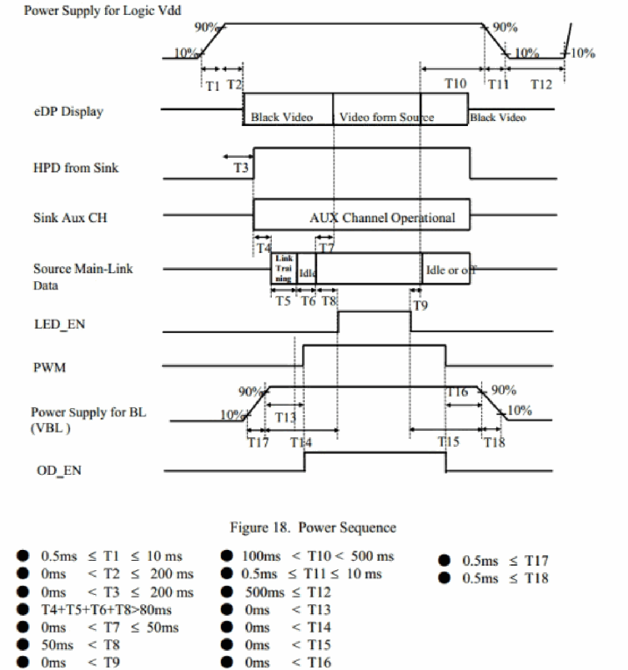
For cases where all timing requirements are met according to the Datasheet but there are still AUX errors, you can appropriately extend T3 (as shown in the figure, even exceeding the required ≤ 200), i.e., prepare-delay- ms, to ensure the Sink end is ready before the Source initiates AUX communication, such as:
&panel {
   prepare-delay-ms = <500>;
}
GPIO HPD
In GPIO HPD mode, in addition to the aforementioned power-on sequence checks, it is also necessary to confirm whether the designated HPD PIN is occupied by other modules. You can use the command cat /d/gpio to confirm:
console:/ # cat /d/gpio
gpiochip1: GPIOs 32-63, parent: platform/ff730000.gpio1, gpio1:
 gpio-33 (            |?              ) out lo

 gpio-34 (            |int-n          ) in hi
 gpio-45 (            |enable         ) out lo
 gpio-46 (            |vsel           ) out lo
 gpio-49 (            |vsel           ) out lo
 gpio-50 (            |vbus-5v        ) out lo
 gpio-55 (            |reset          ) out lo
... ...
gpiochip5: GPIOs 511-511, parent: platform/rk805-pinctrl, rk817-gpio, can sleep:
Additionally, GPIO HPD can also ensure stable recognition of the HPD signal through Pin pull-down configuration, refer to HPD Configuration.
6.3.4 Check AUX Hardware Design
Confirm whether the positive and negative poles of the AUX differential lines are reversed. If reversed due to hardware design oversight, refer to the following modifications:
U-Boot:
diff --git a/drivers/video/drm/analogix_dp_reg.c b/drivers/video/drm/analogix_dp_reg.c
index 292a5076705..373189e9157 100644

--- a/drivers/video/drm/analogix_dp_reg.c
+++ b/drivers/video/drm/analogix_dp_reg.c
@@ -1241,7 +1241,7 @@ ssize_t analogix_dp_aux_transfer(struct drm_dp_aux *aux, struct
drm_dp_aux_msg *
      }

      /* Enable AUX CH operation */
-     reg = AUX_EN;
+     reg = AUX_EN | 0x4;

      /* Zero-sized messages specify address-only transactions. */
      if (msg->size < 1)
Kernel:
diff --git a/drivers/gpu/drm/bridge/analogix/analogix_dp_reg.c b/drivers/gpu/drm/bridge/analogix/analogix_dp_reg.c
index 810b5a2f6041..2dbde10033c5 100644

--- a/drivers/gpu/drm/bridge/analogix/analogix_dp_reg.c
+++ b/drivers/gpu/drm/bridge/analogix/analogix_dp_reg.c
@@ -1202,7 +1202,7 @@ ssize_t analogix_dp_transfer(struct analogix_dp_device *dp,
      }

      /* Enable AUX CH operation */
-     reg = AUX_EN;
+     reg = AUX_EN | 0x4;

      /* Zero-sized messages specify address-only transactions. */
      if (msg->size < 1)
For eDP v1.2 and above versions of AUX link hardware design, the pull-up and pull-down resistors on the AUX differential lines should be removed. If there are still AUX error exceptions, you can try reducing the series capacitance of the AUX signal lines.
6.4 Error Analysis and Solutions for Link Training
eDP Link Training errors are as follows:
# Link Training CR(Clock Recovery) phase failure
[ 1410.198900][ T318] rockchip-dp fdec0000.edp: CR Max reached (0,3,0)

[ 1410.202213][ T318] rockchip-dp fdec0000.edp: LT CR failed!
[ 1410.202227][ T318] rockchip-dp fdec0000.edp: eDP link training failed (-5)
[ 1410.202238][ T318] rockchip-dp fdec0000.edp: unable to do link train, ret=-5

# Link Training EQ(Channel Equalization) phase failure
[ 6673.100385][ T318] rockchip-dp fdec0000.edp: EQ Max loop
[ 6673.101511][ T318] rockchip-dp fdec0000.edp: LT EQ failed!
[ 6673.101515][ T318] rockchip-dp fdec0000.edp: eDP link training failed (-5)
[ 6673.101517][ T318] rockchip-dp fdec0000.edp: unable to do link train, ret=-5
[ 6673.101522][ T318] [drm:analogix_dp_bridge_atomic_enable] ERROR dp commit error, ret = -5
[ 6673.101533][ T318] rockchip-dp fdec0000.edp: failed to set bridge, retry: 0
The main loop code for eDP Link Training is roughly as follows, with variations between different versions:
while (!retval && !training_finished) {
   switch (dp->link_train.lt_state) {

      case START:
         retval = analogix_dp_link_start(dp);
         if (retval)
           dev_err(dp->dev, "LT link start failed!\n");
         break;
      case CLOCK_RECOVERY:
         retval = analogix_dp_process_clock_recovery(dp);
         if (retval)
           dev_err(dp->dev, "LT CR failed!\n");
         break;
      case EQUALIZER_TRAINING:
         retval = analogix_dp_process_equalizer_training(dp);

         if (retval)
           dev_err(dp->dev, "LT EQ failed!\n");
         break;
      case FINISHED:
         training_finished = 1;
         break;
      case FAILED:
         return -EREMOTEIO;
   }
}
eDP Link Training can be divided into three stages in the driver: START, CLOCK_RECOVERY, and EQUALIZER_TRAINING:
START: Initialization of training start parameters.
CLOCK_RECOVERY: Link clock recovery.
EQUALIZER_TRAINING: Link equalization.
The phase where Link Training fails can be determined from the Log.
6.4.1 Confirm Panel Protocol Support
Compare the protocol support for the eDP interface on RK platforms as described in the Functional Features section with the protocol version indicated in the eDP Panel Datasheet. The protocol version supported by the eDP interface must be greater than or equal to the protocol version of the Panel.
6.4.2 Checking Main Link Hardware Design
Ensure that each Lane of Main Link has a one-to-one correspondence at both the Source and Sink ends. If there is a mistake in the hardware design, refer to the following adjustments to modify the correspondence of Lanes:
&edp0 {
   data-lanes = <3 2 1 0>;

};
Verify that the Main Link hardware design complies with the specifications. Refer to the official hardware design guide of the RK platform, for example, the “Rockchip RK3576 Hardware Design Guide” for RK3576.
6.4.3 Checking the Screen Cable and Interface on Hardware for Compliance
The specifications and standards for screen cables and interfaces need to be confirmed with the screen manufacturer, common requirements include:
The screen cable length should not exceed 30cm
The screen cable should have shielding design on the hardware
The connection between the screen cable and interface must be correct and stable
6.4.4 Confirming HPD Status and Power-Up Sequence
As previously mentioned in “Confirming HPD Status and Power-Up Sequence”.
6.4.5 Modify Pre-emphasis and Voltage Swing Configuration
PE (Pre-emphasic, pre-emphasis) and VS (Voltage Swing, voltage swing) configurations are significant factors affecting the quality of eDP signals. The combination of their configurations is as follows:
| Voltage Swing Level | Pre-emphasis Level 0 Vdiff_pre_pp | Pre-emphasis Level 1 Vdiff_pre_pp | Pre-emphasis Level 2 Vdiff_pre_pp | Pre-emphasis Level 3 Vdiff_pre_pp |
|---|---|---|---|---|
| 0 | Required | Required | Required | Optional |
| 1 | Required | Required | Required | Not allowed |
| 2 | Required | Required | Not allowed | Not allowed |
| 3 | Optional | Not allowed | Not allowed | Not allowed |
6.4.5.1 Modify Initial Configuration
The eDP protocol specifies the initial configuration as PE Level 0/ VS Level 0. Different combinations can be attempted by modifying the following PE/VS initial configuration, with the parameters defined as follows:
# define DP_TRAIN_MAX_SWING_REACHED (1 << 2)
# define DP_TRAIN_VOLTAGE_SWING_LEVEL_0 (0 << 0)
# define DP_TRAIN_VOLTAGE_SWING_LEVEL_1 (1 << 0)

# define DP_TRAIN_VOLTAGE_SWING_LEVEL_2 (2 << 0)
# define DP_TRAIN_VOLTAGE_SWING_LEVEL_3 (3 << 0)

# define DP_TRAIN_PRE_EMPHASIS_MASK (3 << 3)
# define DP_TRAIN_PRE_EMPH_LEVEL_0 (0 << 3)
# define DP_TRAIN_PRE_EMPH_LEVEL_1 (1 << 3)
# define DP_TRAIN_PRE_EMPH_LEVEL_2 (2 << 3)
# define DP_TRAIN_PRE_EMPH_LEVEL_3 (3 << 3)
Uboot reference modification as follows:
diff --git a/drivers/video/drm/analogix_dp.c b/drivers/video/drm/analogix_dp.c
index c4b50018baa..0afb116104f 100644
--- a/drivers/video/drm/analogix_dp.c

+++ b/drivers/video/drm/analogix_dp.c
@@ -240,8 +240,8 @@ static int analogix_dp_link_start(struct analogix_dp_device *dp)
      /* Set TX voltage-swing and pre-emphasis to minimum */
      for (lane = 0; lane < lane_count; lane++)
           dp->link_train.training_lane[lane] =
-                      DP_TRAIN_VOLTAGE_SWING_LEVEL_0 |
-                      DP_TRAIN_PRE_EMPH_LEVEL_0;
+                      DP_TRAIN_VOLTAGE_SWING_LEVEL_2 |
+                      DP_TRAIN_PRE_EMPH_LEVEL_1;
      analogix_dp_set_lane_link_training(dp);

      /* Set training pattern 1 */

@@ -254,8 +254,8 @@ static int analogix_dp_link_start(struct analogix_dp_device *dp)
           return retval;

      for (lane = 0; lane < lane_count; lane++)
-          buf[lane] = DP_TRAIN_PRE_EMPH_LEVEL_0 |
-                   DP_TRAIN_VOLTAGE_SWING_LEVEL_0;
+          buf[lane] = DP_TRAIN_PRE_EMPH_LEVEL_1 |
+                   DP_TRAIN_VOLTAGE_SWING_LEVEL_2;

      retval = drm_dp_dpcd_write(&dp->aux, DP_TRAINING_LANE0_SET, buf,
                         lane_count);
Kernel reference modification as follows:
diff --git a/drivers/gpu/drm/bridge/analogix/analogix_dp_core.c b/drivers/gpu/drm/bridge/analogix/analogix_dp_core.c

index 4015073bbb39..10407e67c95f 100644
--- a/drivers/gpu/drm/bridge/analogix/analogix_dp_core.c
+++ b/drivers/gpu/drm/bridge/analogix/analogix_dp_core.c
@@ -435,8 +435,8 @@ static int analogix_dp_link_start(struct analogix_dp_device *dp)
      /* Set TX voltage-swing and pre-emphasis to minimum */
      for (lane = 0; lane < lane_count; lane++)
           dp->link_train.training_lane[lane] =
-                            DP_TRAIN_VOLTAGE_SWING_LEVEL_0 |
-                            DP_TRAIN_PRE_EMPH_LEVEL_0;
+                            DP_TRAIN_VOLTAGE_SWING_LEVEL_2 |
+                            DP_TRAIN_PRE_EMPH_LEVEL_1;
      analogix_dp_set_lane_link_training(dp);


      /* Set training pattern 1 */
@@ -450,8 +450,8 @@ static int analogix_dp_link_start(struct analogix_dp_device *dp)
           return retval;

      for (lane = 0; lane < lane_count; lane++)
-          buf[lane] = DP_TRAIN_PRE_EMPH_LEVEL_0 |
-                   DP_TRAIN_VOLTAGE_SWING_LEVEL_0;
+          buf[lane] = DP_TRAIN_PRE_EMPH_LEVEL_2 |
+                   DP_TRAIN_VOLTAGE_SWING_LEVEL_1;


      retval = drm_dp_dpcd_write(&dp->aux, DP_TRAINING_LANE0_SET, buf,
                         lane_count);
6.4.5.2 Add Settings for Printing
It should be noted that if the initial Link Training fails after setting the Voltage_swing and Pre-emphasis parameters, the next round of Link Training will be based on the parameters recommended by the Panel. You can refer to the following to add printing to determine the subsequent settings for pre-emphasis and voltage swing parameters. The Uboot reference is as follows:
diff --git a/drivers/video/drm/analogix_dp_reg.c b/drivers/video/drm/analogix_dp_reg.c
index d2cb10cc0e..c96495f5e9 100644
--- a/drivers/video/drm/analogix_dp_reg.c

+++ b/drivers/video/drm/analogix_dp_reg.c
@@ -1002,6 +1002,7 @@ void analogix_dp_set_lane_link_training(struct analogix_dp_device *dp)
               DP_TRAIN_PRE_EMPHASIS_SHIFT;
           phy_cfg.dp.voltage[lane] = vs;
           phy_cfg.dp.pre[lane] = pe;
+          printf("[Link Training] vs = %d pe = %d\n", vs, pe);
      }

      phy_cfg.dp.lanes = dp->link_train.lane_count;
Kernel reference is as follows:
diff --git a/drivers/gpu/drm/bridge/analogix/analogix_dp_reg.c b/drivers/gpu/drm/bridge/analogix/analogix_dp_reg.c
index 42d1cbe28b40..ea5657770cfb 100644

--- a/drivers/gpu/drm/bridge/analogix/analogix_dp_reg.c
+++ b/drivers/gpu/drm/bridge/analogix/analogix_dp_reg.c
@@ -733,10 +733,14 @@ void analogix_dp_set_lane_link_training(struct analogix_dp_device *dp)
      u8 lane;
      int ret;

-     for (lane = 0; lane < dp->link_train.lane_count; lane++)
+     for (lane = 0; lane < dp->link_train.lane_count; lane++) {
           analogix_dp_write(dp,
                         ANALOGIX_DP_LN0_LINK_TRAINING_CTL + 4 * lane,
                         dp->link_train.training_lane[lane]);
+          printk("[Link Training] vs = %d pe = %d\n",

+                       (dp->link_train.training_lane[lane] &
DP_TRAIN_VOLTAGE_SWING_MASK) >> DP_TRAIN_VOLTAGE_SWING_SHIFT,
+                       (dp->link_train.training_lane[lane] &
DP_TRAIN_PRE_EMPHASIS_MASK) >> DP_TRAIN_PRE_EMPHASIS_SHIFT);
+     }
if (dp->phy) {
     union phy_configure_opts phy_cfg;
6.4.6 Attempting to Reduce Speed
For details on bandwidth calculation methods, refer to the previous section Bandwidth Calculation Method.
When the bandwidth is sufficient, attempts can be made to reduce the Link Rate, with reference to the DTS configuration as follows:
&edp {
   force-hpd;

   status = "okay";
   ports {
      port@1 {
         reg = <1>;
         edp_out: endpoint {
           link-frequencies = <2700000000>;
           remote-endpoint = <&panel_in>;
         };
      };
   };
};
Alternatively, by forcibly specifying the Link Rate in the driver, the Link Rate macro definitions are as follows:
# define DP_LINK_BW_1_62  0x06
# define DP_LINK_BW_2_7 0x0a
# define DP_LINK_BW_5_4 0x14

# define DP_LINK_BW_8_1 0x1e
U-Boot reference modification:
diff --git a/drivers/video/drm/analogix_dp.c b/drivers/video/drm/analogix_dp.c
index c4b50018baa..35daf949017 100644

--- a/drivers/video/drm/analogix_dp.c
+++ b/drivers/video/drm/analogix_dp.c
@@ -665,6 +665,7 @@ static int analogix_dp_get_max_rx_bandwidth(struct analogix_dp_device
*dp,

           *bandwidth = data;
      }
+     *bandwidth = DP_LINK_BW_1_62;

      return 0;
 }
Kernel reference modification:
diff --git a/drivers/gpu/drm/bridge/analogix/analogix_dp_core.c b/drivers/gpu/drm/bridge/analogix/analogix_dp_core.c
index 4015073bbb39..f70898e0319e 100644

--- a/drivers/gpu/drm/bridge/analogix/analogix_dp_core.c
+++ b/drivers/gpu/drm/bridge/analogix/analogix_dp_core.c
@@ -851,6 +851,7 @@ static int analogix_dp_get_max_rx_bandwidth(struct analogix_dp_device
*dp,

           *bandwidth = data;
      }
+     *bandwidth = DP_LINK_BW_1_62;

      return 0;
 }
6.4.7 Increase the Retry Count during the CR/EQ Phase
In the eDP protocol, the maximum number of Retries during the CR/EQ phase is 5, but some specific displays may require more Retries to ensure the success of Link Training.
U-Boot reference modification is as follows:
diff --git a/drivers/video/drm/analogix_dp.h b/drivers/video/drm/analogix_dp.h
index c6cb113190e..f9312f7391d 100644
--- a/drivers/video/drm/analogix_dp.h

+++ b/drivers/video/drm/analogix_dp.h
@@ -460,9 +460,9 @@
 /* ANALOGIX_DP_LINK_POLICY */
 #define ALTERNATE_SR_ENABLE       (0x1 << 7)

-#define DP_TIMEOUT_LOOP_COUNT 100
-#define MAX_CR_LOOP 5
-#define MAX_EQ_LOOP 5
+#define DP_TIMEOUT_LOOP_COUNT 200
+#define MAX_CR_LOOP 10
+#define MAX_EQ_LOOP 10

 /* I2C EDID Chip ID, Slave Address */

 #define I2C_EDID_DEVICE_ADDR      0x50
Kernel reference modification is as follows:
diff --git a/drivers/gpu/drm/bridge/analogix/analogix_dp_core.h b/drivers/gpu/drm/bridge/analogix/analogix_dp_core.h
index 879a56eab2b7..8d493a0f76d1 100644

--- a/drivers/gpu/drm/bridge/analogix/analogix_dp_core.h
+++ b/drivers/gpu/drm/bridge/analogix/analogix_dp_core.h
@@ -13,9 +13,9 @@
 #include <drm/drm_crtc.h>
 #include <drm/drm_bridge.h>
-#define DP_TIMEOUT_LOOP_COUNT 100
-#define MAX_CR_LOOP 5

-#define MAX_EQ_LOOP 5
+#define DP_TIMEOUT_LOOP_COUNT 200
+#define MAX_CR_LOOP 10
+#define MAX_EQ_LOOP 10
 #define MAX_PLL_LOCK_LOOP 5

 /* Training takes 22ms if AUX channel comm fails. Use this as retry interval */
6.4.8 Adding Reset Panel Operations
U-Boot reference modifications are as follows:
diff --git a/drivers/video/drm/analogix_dp.c b/drivers/video/drm/analogix_dp.c
index c4b50018baa..91ff3fa2ae6 100644
--- a/drivers/video/drm/analogix_dp.c

+++ b/drivers/video/drm/analogix_dp.c
@@ -715,6 +715,12 @@ static int analogix_dp_init_training(struct analogix_dp_device *dp,
      /* All DP analog module power up */
      analogix_dp_set_analog_power_down(dp, POWER_ALL, 0);

+     if (dp->connector.panel->funcs->unprepare)
+          dp->connector.panel->funcs->unprepare(dp->connector.panel);
+
+     if (dp->connector.panel->funcs->prepare)
+          dp->connector.panel->funcs->prepare(dp->connector.panel);
+
      return 0;

 }
Kernel reference modifications are as follows:
diff --git a/drivers/gpu/drm/bridge/analogix/analogix_dp_core.c b/drivers/gpu/drm/bridge/analogix/analogix_dp_core.c
index 4015073bbb39..4dfc04a6ccae 100644

--- a/drivers/gpu/drm/bridge/analogix/analogix_dp_core.c
+++ b/drivers/gpu/drm/bridge/analogix/analogix_dp_core.c
@@ -910,6 +910,11 @@ static int analogix_dp_full_link_train(struct analogix_dp_device *dp,
      /* All DP analog module power up */
      analogix_dp_set_analog_power_down(dp, POWER_ALL, 0);

+     if (dp->plat_data->panel) {
+          analogix_dp_panel_unprepare(dp);
+          analogix_dp_panel_prepare(dp);
+     }
+
      dp->link_train.lt_state = START;
/* Process here */
6.4.9 Attempting Forced Output
If the above methods all fail to successfully perform Link Training, you can also try forced output to confirm the issue.
U-Boot reference modification is as follows:
diff --git a/drivers/video/drm/analogix_dp.c b/drivers/video/drm/analogix_dp.c
index c4b50018baa..5cf45165698 100644

--- a/drivers/video/drm/analogix_dp.c
+++ b/drivers/video/drm/analogix_dp.c
@@ -1035,6 +1035,7 @@ static int analogix_dp_connector_enable(struct rockchip_connector
*conn,
      u32 fmt_id;
      u32 val;
      int ret;
+     int i;

      drm_mode_copy(&video->mode, &conn_state->mode);

@@ -1097,8 +1098,11 @@ static int analogix_dp_connector_enable(struct rockchip_connector
*conn,

      ret = analogix_dp_set_link_train(dp, dp->video_info.max_lane_count,
                              dp->video_info.max_link_rate);
      if (ret) {
-          dev_err(dp->dev, "unable to do link train\n");
-          return ret;
+          dev_err(dp->dev, "unable to do link train, using default strength\n");
+          for (i = 0; i < dp->link_train.lane_count; i++) {
+                dp->link_train.training_lane[i] = DP_TRAIN_VOLTAGE_SWING_LEVEL_0 |
DP_TRAIN_PRE_EMPH_LEVEL_0;
+          }
+          analogix_dp_set_lane_link_training(dp);
      }


      ret = analogix_dp_enable_scramble(dp, 1);
Kernel reference modification is as follows:
diff --git a/drivers/gpu/drm/bridge/analogix/analogix_dp_core.c b/drivers/gpu/drm/bridge/analogix/analogix_dp_core.c
index 4015073bbb39..b97cd40ef205 100644

--- a/drivers/gpu/drm/bridge/analogix/analogix_dp_core.c
+++ b/drivers/gpu/drm/bridge/analogix/analogix_dp_core.c
@@ -1341,6 +1341,7 @@ static int analogix_dp_commit(struct analogix_dp_device *dp)
 {
      struct video_info *video = &dp->video_info;
      int ret;
+     int i;
      ret = drm_dp_read_dpcd_caps(&dp->aux, dp->dpcd);
      if (ret < 0) {

@@ -1362,8 +1363,10 @@ static int analogix_dp_commit(struct analogix_dp_device *dp)

      ret = analogix_dp_train_link(dp);
      if (ret) {
-          dev_err(dp->dev, "unable to do link train, ret=%d\n", ret);
-          return ret;
+          dev_err(dp->dev, "unable to do link train, using default strength\n");
+          for (i = 0; i < dp->link_train.lane_count; i++)
+                dp->link_train.training_lane[i] = DP_TRAIN_VOLTAGE_SWING_LEVEL_0 |
DP_TRAIN_PRE_EMPH_LEVEL_0;
+          analogix_dp_set_lane_link_training(dp);
      }


      ret = analogix_dp_enable_scramble(dp, 1);
Note: The above forced output method does not comply with the eDP protocol specification. If the screen can be lit, there may still be hidden dangers. It is recommended to contact the screen manufacturer for further analysis.
6.5 Display Anomalies (Training Successful) Analysis and Solutions
If Link Training has been successful and yet the display remains black or exhibits anomalies, please attempt the following DEBUG methods in sequence.
6.5.1 Enable Self-Test Mode
For details, refer to the sections Panel Self-Test Mode and Controller Self-Test Mode.
6.5.2 Confirm if the VOP Status Meets Expectations
For details, refer to the section “Check VOP Status” above.
6.5.3 Verify if the Clock Configuration Meets Expectations
Refer to the previous section “View Clock Configuration”.
6.6 How to Optimize Signal Quality
6.6.1 Optimizing PE/VS Level Configuration
For details, refer to the section “Modifying PE/VS Configuration”.
6.6.2 Enabling SSC Feature
SSC (Spread Spectrum Clocking) can reduce electromagnetic interference (EMI) and mitigate the impact of power supply noise, thereby optimizing signal integrity.
The RK platform will enable this feature by default when Sink end supports SSC functionality. The detection function for SSC feature is as follows, and you can add prints to check if it is supported:
bool analogix_dp_ssc_supported(struct analogix_dp_device *dp)
{
   /* Check if SSC is supported by both sides */

   return dp->plat_data->ssc && dp->link_train.ssc;
}
If you need to forcibly enable the SSC feature, simply let the above function return True. Both Uboot and Kernel need to be modified simultaneously.