
ArmSoM applicability
This is a vendor platform reference, not an ArmSoM test report. Official ArmSoM documentation identifies Sige7 as RK3588, Sige3 as RK3568B2, and Sige5/CM5 as RK3576. The corresponding SoC chapters may inform those platforms, but verify the board’s actual display interfaces, SDK/BSP branch, device tree and kernel patches. The source covers Linux 4.4, 4.19, 5.10 and 6.1 as listed below; kernel version alone does not establish that a mainline kernel contains these vendor features. Target hardware, register, clock, memory and voltage changes have not been validated.
Sources: the Chinese and English Rockchip DRM Display Driver Developer Guide both identify V5.9.0; the Chinese PDF has 81 pages and the English PDF 87. Chinese follows the Chinese original; English and Russian follow the English original. Chapter numbering matches, but table layout, terminology and example wording differ; see the editorial notes. Chinese uses all 55 original Chinese-PDF figures; English and Russian use all 55 original English-PDF figures, stored as independent files. Nontechnical cover material, intended audience and revision history are omitted; technical versions and all 12 chapters are retained. Check board adaptation against the official ArmSoM documentation.
Reading note: the parameters and logs below are source examples, not ArmSoM measurements. Source uncertainties include the 600MHz boundary, PLL frequency-division wording, layer-allocation counts and filenames. Original technical information is retained and individually recorded in the editorial notes. Voltage, clock, IOMMU and register changes require verification against the target BSP and hardware limits; do not apply them directly to a production device.
Preface and product versions
This guide describes the basic characteristics, workflow and common problems of the Rockchip processor’s VOP and display interfaces under the DRM framework. Its purpose is to improve understanding of the DRM display-driver framework and hardware interfaces and enable quicker diagnosis and resolution of common issues.
| Chip | Kernel version |
|---|---|
| RK3036 | Linux kernel 4.4 or later |
| RK312X/PX3SE | Linux kernel 4.4 or later |
| RK3288 | Linux kernel 4.4 or later |
| RK322X/RK312XH | Linux kernel 4.4 or later |
| RK3308 | Linux kernel 4.4 or later |
| RK322XH/RK332X | Linux kernel 4.4 or later |
| RK3326/PX30 | Linux kernel 4.4 or later |
| RK3368/PX5 | Linux kernel 4.4 or later |
| RK3399 | Linux kernel 4.4 or later |
| RK1808 | Linux kernel 4.4 or later |
| RV1109/RV1126 | Linux kernel 4.19 or later |
| RK356X | Linux kernel 4.19 or later |
| RK3588 | Linux kernel 5.10 or later |
| RV1103/RV1106 | Linux kernel 5.10 or later |
| RK3528 | Linux kernel 4.19 or later |
| RK3562 | Linux kernel 5.10 or later |
| RK3576 | Linux kernel 6.1 or later |
| RK3506 | Linux kernel 6.1 or later |
| RV1126B | Linux kernel 6.1 or later |
1. Overview of Rockchip Platform Display Sub-system (DSS)
The display sub-system is a general term for the software and hardware systems related to display output on the Rockchip platform. It includes VOP (LCDC in older platforms, such as RK3188 and RK3066), and display signal output modules such as RGB, BT1120, BT656, I8080 (MCU display interface), LVDS, MIPI DSI, EDP, DP, HDMI, as well as their corresponding software drivers.
The hardware framework of the entire display system is shown in the following figure:
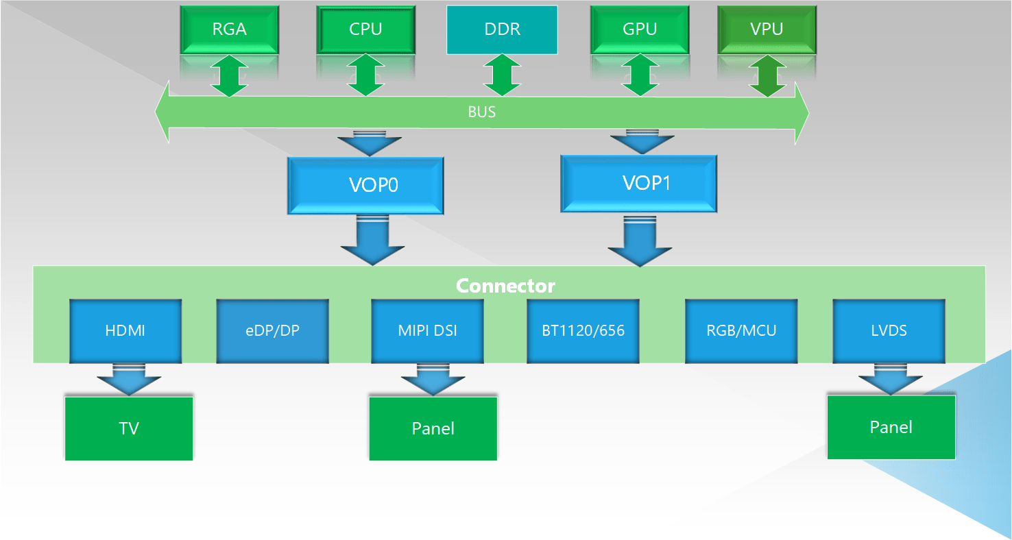
VOP 1.0 Display Sub-system Architecture
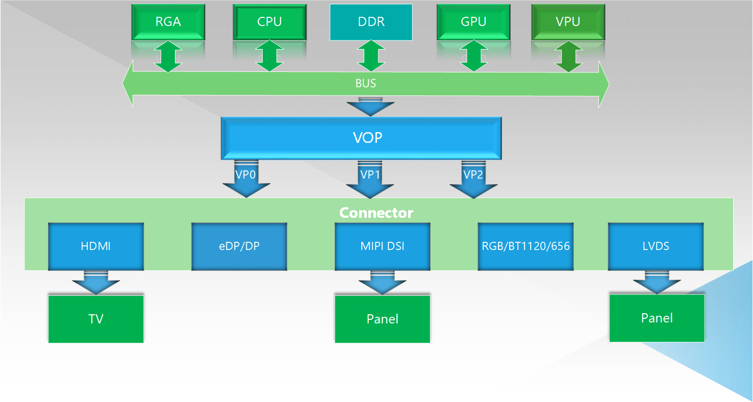
VOP 2.0 Display Sub-system Architecture
As can be seen from the above DSS block diagram, at the end of the entire display path, there is a display graphics acceleration module composed of RGA, GPU, and VPU. These are hardware IPs optimized for image processing, which can efficiently generate and further process images (for example, the GPU provides image rendering functions through the OpenGL function, the RGA can perform 2D processing such as zooming, rotating, and compositing image data, and the VPU can efficiently perform video decoding), thus reducing the burden on the CPU.
The data processed by these image acceleration modules is stored in the DDR, and then read by the VOP. After processing such as Alpha overlay, color space conversion, gamma correction, and HDR conversion according to application requirements, it is sent to the corresponding display interface module (HDMI/DP/DSI/RGB/LVDS). These interface modules convert the received data into data streams that conform to their respective protocols and send them to the display or screen, presenting to the end-user.
Currently, there are two VOP architectures on the Rockchip platform-VOP 1.0 and VOP 2.0. The main difference between them is the way they support multiple displays. VOP 1.0 uses multiple VOPs to achieve multi-screen display. That is, in normal case, one VOP can only output one independent display timing at the same time, driving one screen to display independent content. If dual- screen display is required, two VOPs are needed. Therefore, on platforms that support dual-screen display, such as RK3288, RK3399, and PX30, there are two independent VOPs.
VOP 2.0 adopts a unified display architecture, that is, there is only one VOP on the entire SOC, but at the rear end of the VOP, there are multiple independent Video Port (abbreviated as VP) output interfaces. These VPs can work independently at the same time and output independent display timings. For example, in the above VOP 2.0 block diagram, with three VPs, three-screen different- display can be achieved simultaneously.
If you want to know which chips adopt the VOP 1.0 architecture and which chips adopt the VOP 2.0 architecture, please refer to the content of the Display Feature chapter later.
2. Overview of DRM
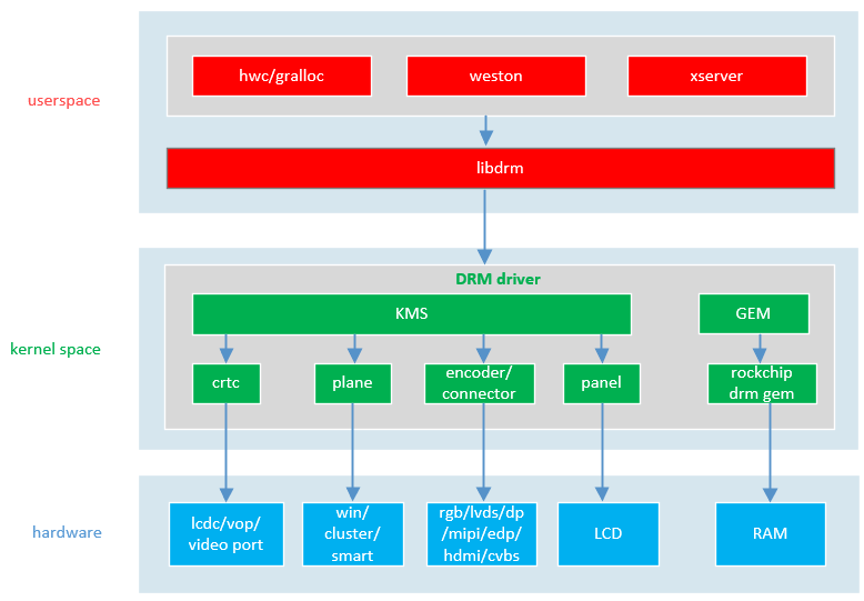
DRM stands for Direct Rendering Manager, which manages display output, buffer allocation, and frame buffering. The corresponding userspace library is libdrm. The libdrm library provides a series of friendly control encapsulations, enabling users to easily control the display and apply for buffers. The device node of DRM is “/dev/dri/cardX”, where X is a value from 0-15, and /dev/dri/card0 is used by default.
Since the Linux 4.4 kernel, the display drivers on the Rockchip platform have all switched to the DRM display framework.
It should be noted that in a system, there may be multiple DRM devices, and the device nodes /dev/dri/cardX generated by these devices are not fixed. They are related to the loading order of the DRM drivers.
For example, on the current Rockchip platforms, both the display sub-system and the NPU driver use the DRM framework. Therefore, in most cases, we will see two device nodes on the system: /dev/dri/card0 and /dev/dri/card1 . However, there is no fixed correspondence between card0, card1 and the display sub-system and NPU. Generally, the driver that is loaded first will be registered as card0.
If an application needs to open a DRM display device, after opening /dev/dri/card0 or /dev/dri/card1 , the application needs to make further judgments to determine whether the device is a display device. On the Rockchip platform, there are currently two methods:
-
Use the drmIsKMS(int fd) API provided by libdrm to check the opened device and determine whether the device supports the display function. NPU devices do not support the display function.
-
Use the drmOpen(“rockchip”, NULL) provided by libdrm to force-open the rockchip drm driver.
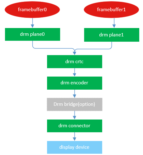
2.1 Basic Concepts
To facilitate the management of various hardware modules on the display path, DRM defines the following concepts:
| Basic Concept |
Description |
|---|---|
| CRTC | Display controller. On the rockchip platform, it is an abstraction of the SOC internal VOP (LCDC in some documents) module or the Video Port in VOP2 |
| Plane | Layer. On the rockchip platform, it is an abstraction of the win layer in the SOC internal VOP (LCDC) module |
| Encoder | Output converter, referring to display interfaces such as RGB, LVDS, DSI, eDP, DP, HDMI, CVBS, VGA |
| Connector | The interface part for interaction between the encoder and the panel |
| Bridge | Bridging device, generally used to register a conversion chip connected after the encoder, such as a DSI2HDMI conversion chip |
| Panel | Generally refers to the screen, an abstraction of various LCD display devices |
| GEM | Buffer management and allocation under DRM, similar to ION, DMA BUFFER |
2.2 Display Path
2.3 Interaction Process between DRM Driver and libdrm
3. Software Drivers
3.1 U-Boot Driver
The display driver in U-Boot mainly provides two functions: booting logo display and charging interface display.
On the Rockchip platform, the booting logo is generally divided into two stages: displaying the U-Boot logo and displaying the Kernel logo.

Default U-Boot logo
Default Kernel logo
These two LOGO pictures are placed in the root directory of the Linux kernel by default (logo.bmp and logo_kernel.bmp). When the Linux Kernel is compiled, they will be packaged into resource.img and then into Boot.img.
When U-Boot starts, it loads these two files into memory. The U-Boot LOGO is displayed during the U-Boot stage, and the address of the Kernel LOGO in memory is passed by U-Boot to the Linux kernel, which is displayed during the initialization stage of the Linux Kernel’s drm driver.
3.1.1 Driver Directory
drivers/video/drm/
3.1.2 Driver Files
| Driver | File |
|---|---|
| Core | rockchip_display.c rockchip_crtc.c rockchip_connector.c rockchip_phy.c rockchip_panel.c rockchip_bridge.c |
| VOP | rockchip_vop.c rockchip_vop_reg.c rockchip_vop2.c rockchip_vop2_reg.c |
| RGB | rockchip_rgb.c inno_video_combo_phy.c |
| LVDS | rockchip_lvds.c inno_video_combo_phy.c |
| MIPI-DSI | drm_mipi_dsi.c dw_mipi_dsi2.c inno_mipi_phy.c inno_video_combo_phy.c samsung_mipi_dcphy.c |
| eDP | rockchip_analogix_dp.c rockchip_analogix_dp_reg.c |
| HDMI | dw_hdmi.c rockchip_dw_hdmi.c rockchip-inno-hdmi-phy.c inno_hdmi.c dw_hdmi_qp.c rockchip_dw_hdmi_qp.c phy-rockchip-samsung-hdptx-hdmi.c |
| TVE /CVBS | rockchip_drm_tve.c |
| DP | dw-dp.c drm_dp_helper.c phy-rockchip-usbdp.c |
The above driver files may be slightly adjusted in different U-Boot versions, but most of the driver files and framework parts remain basically unchanged. You can adjust according to the actual situation when referring.
3.1.3 Interface Description
1. Display U-Boot logo
void rockchip_show_logo(void)
2. Display a specified bmp picture, which is mainly used for displaying the charging logo currently
void rockchip_show_bmp(const char *bmp)
3. Pass some variables determined in U-Boot to the kernel by modifying the dtb file, including the size, address, format, output
scan timing, and over-scan configuration of the kernel logo, etc.
void rockchip_display_fixup(void *blob)
3.1.4 Logo Display Application Description
1. Enable U-Boot logo
The logo is controlled by the route_xxx node of the corresponding display interface in the Linux kernel dts (the U-Boot display module and the Linux kernel share the same dtb). Here, xxx can be dsi, edp, hdmi, lvds. Specifically, please search for the route keyword in the dts.
Taking MIPI DSI0 as an example, find the route_dsi0 node in the corresponding board-level dts file and set the status to “okay”:
&route_dsi0 {
     status = "okay";
     connect = <&vp3_out_dsi0>;
};
The connect attribute refers to the detailed description in the DTS Configuration chapter later.
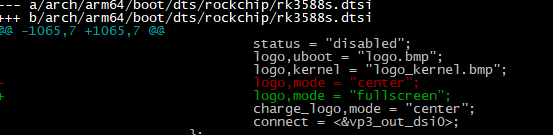
2. Configure U-Boot logo to be displayed full-screen
The logo is centered by default. If full-screen display is required, modify the route node of the corresponding interface.
For example, if you need to display the logo output on DSI0 full-screen, modify the logo,mode attribute of route_dis0 to “fullscreen”.
3. Logo picture requirements
The U-Boot logo and the Linux Kernel logo have the same resolution. Since the VOP virtual width is in units of words, the width of the resolution must be aligned to 4 pixels. For screens that are not 4-pixel-aligned and need to be displayed full-screen, the picture can be aligned down to 4 pixels, and at the same time, configure logo,mode = “fullscreen”
Only 8-bit, 16-bit, 24-bit, and 32-bit bmp pictures are supported;
The U-Boot logo and the Linux Kernel logo must be enabled at the same time, that is, both logo.bmp and logo_kernel.bmp must be provided.
4. Boot log confirmation
If the logo function is enabled and working well, you will see a log similar to the following during the U-Boot stage:
Rockchip UBOOT DRM driver version: v1.0.1
vp0 have layer nr:2[0 2 ], primary plane: 2
vp1 have layer nr:2[1 3 ], primary plane: 3
vp2 have layer nr:2[6 8 ], primary plane: 8
vp3 have layer nr:2[7 9 ], primary plane: 9
Using display timing dts
dsi@fde20000: detailed mode clock 132000 kHz, flags[a]
  H: 1080 1095 1099 1129
  V: 1920 1935 1937 1952
bus_format: 100e
VOP update mode to: 1080x1920p0, type: MIPI0 for VP3
VOP VP3 enable Esmart3[654x270->654x270@213x825] fmt[2] addr[0xedf04000]
final DSI-Link bandwidth: 880000 Kbps x 4
......
hdmi_select_link_config use tmds mode
mode:1920x1080 bus_format:0x100a
hdmi@fde80000: detailed mode clock 148500 kHz, flags[5]
  H: 1920 2008 2052 2200
  V: 1080 1084 1089 1125
bus_format: 100a
VOP update mode to: 1920x1080p0, type: HDMI0 for VP0
......
VOP VP0 enable Esmart0[654x270->654x270@633x405] fmt[2] addr[0xedf04000]
......
CLK: (uboot. arm: enter 1200000 KHz, init 1200000 KHz, kernel 0N/A)
It can be seen that the logo is displayed on both VP0 and VP3.
The display resolution of VP0 is 1920 x 1080, and the display interface is HDMI.
The display resolution of VP3 is 1080 x 1920, and the display interface is MIPI DSI.
The size of the displayed logo is 654 x 270.
5. How to rotate the logo by a fixed angle
If, due to portrait or landscape screen reasons, you want the logo to be rotated by a certain angle for display, you can rotate it on a PC, save it as a new picture, and then replace logo.bmp and kernel_logo.bmp in the kernel project;
6. Split mode logo display
The split mode means that one crtc is connected to two connectors to connect two screens. If you want the left and right screens to display different contents and be spliced into a complete image, you can splice the left and right screen pictures on a PC, save them as a complete image, and then replace logo.bmp and kernel_logo.bmp in the kernel project;
7. How to display only one picture
If you want to display only one picture during the uboot and kernel stages, you can either make logo.bmp and kernel_logo.bmp use the same picture or configure the “logo,uboot” and “logo,kernel” attributes under the route node of the dts file to the same picture;
8. How to support 4K resolution logo display function
The defconfig of each platform cannot support the normal display of 4K logo pictures. The serial port will have a log similar to the following:
......
bmp[logo.bmp] size[23MB] is over the limitation MAX_IMAGE_BYTES[8MB]
failed to display uboot logo
CLK: (uboot. arm: enter 1008000 KHz, init 1008000 KHz, kernel 0N/A)
 bpll 816000 KHz
 lpll 816000 KHz
......
Taking the RK3576 platform as an example, the following modifications are required:
diff --git a/drivers/video/drm/rockchip_display.c b/drivers/video/drm/rockchip_display.c
index b1773ba6942..d1606db1ba5 100644
--- a/drivers/video/drm/rockchip_display.c
+++ b/drivers/video/drm/rockchip_display.c
@@ -52,7 +52,7 @@
#define RK_BLK_SIZE 512
#define BMP_PROCESSED_FLAG 8399
#define BYTES_PER_PIXEL sizeof(uint32_t)
-#define MAX_IMAGE_BYTES (8 * 1024 * 1024)
+#define MAX_IMAGE_BYTES (32 * 1024 * 1024)
DECLARE_GLOBAL_DATA_PTR;
static LIST_HEAD(rockchip_display_list);
diff --git a/include/configs/rk3576_common.h b/include/configs/rk3576_common.h
index 16abba314c5..b4a8ec3b898 100644
--- a/include/configs/rk3576_common.h
+++ b/include/configs/rk3576_common.h
@@ -22,7 +22,7 @@
#endif
#define CONFIG_SPL_LOAD_FIT_ADDRESS 0x42000000

-#define CONFIG_SYS_MALLOC_LEN (32 << 20)
+#define CONFIG_SYS_MALLOC_LEN (32 << 21)
#define CONFIG_SYS_CBSIZE 1024
#ifdef CONFIG_SUPPORT_USBPLUG
And the configuration item CONFIG_DRM_MEM_RESERVED_SIZE_MBYTES needs to be modified to 64 MB.
The reasons for the above modifications are as follows:
(1) Considering memory occupation and the configuration of the default parameter partition table, it is not recommended to use too large a BMP logo picture. Therefore, MAX_IMAGE_BYTES is limited to 8 MB. For pictures larger than this size, BMP pictures in the BI_RLE4/BI_RLE8 format are recommended.
(2) The size of a common 4K BI_RGB 24bpp BMP picture is about 24 MB. The default malloc heap size of each platform is usually 32 MB, and the BMP decode-related functions may not be able to apply for memory.
(3) To ensure a smooth transition from the U-Boot logo to the Kernel logo display, the two logo pictures usually have the same resolution and format. In this way, the memory area size reserved for the logo display function (determined by CONFIG_DRM_MEM_RESERVED_SIZE_MBYTES, which is 32 MB by default) is not enough.
9. How to make different screens display different contents
You can refer to the following method to modify, pack new pictures into resource.img, and modify the corresponding dts file:
--- a/arch/arm64/boot/dts/rockchip/rk3588.dtsi
+++ b/arch/arm64/boot/dts/rockchip/rk3588.dtsi
@@ -854,7 +854,7 @@ &display_subsystem {
     route {
         route_dp1: route-dp1 {
              status = "disabled";
-             logo,uboot = "logo.bmp";
+             logo,uboot = "logo_new.bmp";
              logo,kernel = "logo_kernel.bmp";
              logo,mode = "center";
              charge_logo,mode = "center";
--- a/scripts/mkimg
+++ b/scripts/mkimg
+LOGO_NEW_PATH=${srctree}/logo_new.bmp
+[ -f ${LOGO_NEW_PATH} ] && LOGO_NEW=logo_new.bmp
+
LOGO_KERNEL_PATH=${srctree}/logo_kernel.bmp
[ -f ${LOGO_KERNEL_PATH} ] && LOGO_KERNEL=logo_kernel.bmp
@@ -233,6 +236,9 @@ if [ -x ${srctree}/scripts/bmpconvert ]; then
     if [ -f ${LOGO_PATH} ]; then
         ${srctree}/scripts/bmpconvert ${LOGO_PATH};
     fi
+    if [ -f ${LOGO_NEW_PATH} ]; then
+        ${srctree}/scripts/bmpconvert ${LOGO_NEW_PATH};
+    fi
@@ -242,12 +248,15 @@ if [ "${srctree}" != "${objtree}" ]; then
     if [ -f ${LOGO_PATH} ]; then
         cp -a ${LOGO_PATH} ${objtree}/;
     fi
+    if [ -f ${LOGO_NEW_PATH} ]; then
+        cp -a ${LOGO_NEW_PATH} ${objtree}/;
+    fi
fi
-scripts/resource_tool ${DTB_PATH} ${LOGO} ${LOGO_KERNEL} >/dev/null
-echo " Image: resource.img (with ${DTB} ${LOGO} ${LOGO_KERNEL}) is ready"
+scripts/resource_tool ${DTB_PATH} ${LOGO} ${LOGO_NEW} ${LOGO_KERNEL} >/dev/null
+echo " Image: resource.img (with ${DTB} ${LOGO} ${LOGO_NEW} ${LOGO_KERNEL}) is ready"
3.1.5 Video Console Application Description
This function is used to display the U-Boot startup logs and command-line interface on the screen or monitor. In the 《U-Boot Driver》 chapter, it is mentioned that the Logo display function is divided into two stages: U-Boot Logo and Kernel Logo. After enabling the Video Console function, the U-Boot Logo display will be replaced by the Video Console text display, while the Kernel Logo will still be displayed normally.
DTS configuration: Refer to the DTS configuration description in step 1 of 《Logo Display Application Description》 to enable the U- Boot display function.
defconfig configuration:
Enable Video Console configuration:
/* enable the video console */
CONFIG_ROCKCHIP_VIDCONSOLE=y
Configure the resolution and BPP (Bits Per Pixel) of the Video Console. Taking 1920x1080 16bpp as an example:
/* the resolution of the video console */
CONFIG_ROCKCHIP_VIDCONSOLE_WIDTH=1920
CONFIG_ROCKCHIP_VIDCONSOLE_HEIGHT=1080

/* the bits per pixel the of video console */
CONFIG_ROCKCHIP_VIDCONSOLE_BPP32 is not set
CONFIG_ROCKCHIP_VIDCONSOLE_BPP16=y
CONFIG_ROCKCHIP_VIDCONSOLE_BPP8 is not set
If not specified, the default horizontal resolution is the minimum value of the horizontal resolutions of the corresponding screens or monitors in each display path, and the vertical resolution is also the minimum value of their vertical resolutions. This is to ensure the minimization of the default framebuffer size.
Taking RK3588 as an example, assuming that the output resolution of VP0 HDMI0 is 1920x1080 and the output resolution of VP3 DSI0 is 1080x1920, the default resolution of the Video Console at this time is 1080x1080.
If not specified, the BPP is 32 by default.
Configure the framebuffer size of the Video Console. The calculation formula is:
size = width × height × bpp / (8 × 1024 × 1024)
Taking the configuration of 1920x1080 32bpp as an example:
size = 1920 × 1080 × 32 / (8 × 1024 × 1024) = 8 MB
/* the framebuffer size of video console */
CONFIG_ROCKCHIP_VIDCONSOLE_MEM_RESERVED_SIZE_MBYTES=8
If not specified, the default framebuffer size is 16M. If the framebuffer size required by the Video Console (taking 3840x2160 32bpp as an example) exceeds the default value, there will be an error message as follows and it will fall back to the U-Boot Logo display:
......
video console fb size [33177600 Bytes] is over reserved [16777216 Bytes], then back to show uboot logo
......
3.1.6 Analyze the Screen Flickering or No-Display Problem during the Transition from U-Boot Logo to Linux Kernel Logo
1. Confirm whether the DRM driver is loaded normally
During the loading process of the DRM driver, some resources may not be ready, resulting in the failure of the DRM driver to bind. There may be a log similar to the following:
[1.792387] dw-mipi-dsi2 fde20000.dsi: [drm:dw_mipi_dsi2_bind] *ERROR* Failed to find panel or bridge: -517
This log indicates that the panel or bridge is not ready at this time. The normal driver framework will try to bind again after a period of time. However, if the following log appears finally, it indicates that the drm driver has been loaded successfully. In this case, we don’t need to care too much about the log of one or two binding failures at the beginning:
[2.566831] rockchip-drm display-subsystem: [drm] fb0: rockchipdrmfb frame buffer device
If the startup log keeps showing the binding failure log, you may need to check your dts configuration. In products, the most common issues are that the GPIO port is registered by other devices first, the panel’s compatible is not configured correctly resulting in the failure of panel registration, and the backlight driver registration fails, etc.
If the following logo-related failure information appears in the Linux kernel log, it is necessary to carefully analyze in combination with the code:
rockchip-drm display-subsystem: failed to parse resources for logo display
rockchip-drm display-subsystem: connector[HDMI-A-1] can't found any modes
rockchip-drm display-subsystem: can't not find any logo display
rockchip-drm display-subsystem: failed to show loader logo
2. DDR Frequency Conversion Leading to Screen Flickering or Display Misalignment
(1) Try to close the DDR frequency-conversion node in the dts file to ensure that no DDR frequency conversion is performed in the kernel stage. The modification method is as follows:
&dmc {
  status = "disabled";
};
(2) Try to close the adjustment of the DCLK frequency during DDR frequency conversion. The modification method is as follows:
&dmc {
  vop-dclk-mode = <1>;
};
3. Caused by changes in the clock tree
In some platforms, the clk tree configuration in U-Boot and the kernel are independent. If the clk strategies of the two drivers are inconsistent, screen flickering may occur when the Linux kernel clk is re-initialized. Taking RK3399 as an example, it can be confirmed as follows:
(1) Add while(1); at the entrance of the rk3399_clk_init()@kernel/drivers/clk/rockchip/clk-rk3399.c function to confirm whether there is a screen-flickering problem;
(2) Add while(1) at the end of the rk3399_clk_init()@kernel/drivers/clk/rockchip/clk-rk3399.c function to confirm whether there is a screen-flickering problem;
(3) If there is no screen-flickering phenomenon in step (1) but there is a screen-flickering phenomenon in step (2), it can be basically confirmed that the screen-flickering problem is caused by changes in the clk tree. You can directly contact the person in charge of the corresponding platform cru or submit a redmine and state that it is transferred to the person in charge of pll.
4. Caused by clock shutdown
There may be some problems in the process or software bugs that cause some necessary clocks not to be enabled when the driver is registered. As a result, these clocks are automatically turned off by the framework after the kernel runs, leading to display abnormalities. You can try the following modification to keep the clock on by default for testing:
In the dts file, find the chosen node and add clk_ignore_unused at the end of bootargs, for example: bootargs = “xxxx clk_ignore_unused”;

5. Different Sizes of U-Boot Logo and Kernel Logo Pictures
The Rockchip platform requires that the U-Boot logo and the kernel logo pictures have the same resolution size. If the U- Boot logo is displayed normally but there is an abnormal display in the kernel stage, you can confirm whether the resolutions of logo.bmp and logo_kernel.bmp in the kernel directory are consistent;

6. Some Power GPIOs Re-initialized during Kernel Initialization
There are many possible reasons for this problem. In general, during the porting process of a new project, it is necessary to confirm in a timely manner whether the GPIO power related to display conflicts with other modules;
If the DTS is confirmed to be correct, you can search for keywords in the serial port in the kernel code. Use the binary search method to set a breakpoint at the loading position of each module and gradually confirm the point that causes the screen- flickering problem;
7. VOP Priority Configuration Problem
If the VOP priority is not configured to the highest, it is possible that the bus is preempted by other IPs during the kernel loading stage, resulting in screen flickering. This problem is generally fixed before the SDK is released.
8. Test Related Power and Signals
If the above methods do not find the screen-flickering problem, please use an oscilloscope to capture the waveforms of CLK, DATA, power, and other related signals from the U-Boot to the kernel stage and submit a redmine.
3.2 Kernel Driver
3.2.1 Driver Directory
drivers/gpu/drm/rockchip/
drivers/gpu/drm/bridge/analogix/
drivers/gpu/drm/bridge/synopsys/
drivers/phy/rockchip/
3.2.2 Driver Files
| Driver | File | Doc |
|---|---|---|
| Core | rockchip_drm_drv.c rockchip_drm_fb.c rockchip_drm_fbdev.c rockchip_drm_gem.c rockchip_drm_logo.c rockchip_drm_direct_show.c panel-simple.c |
rockchip-drm.txt or rockchip-drm.yaml |
| VOP | rockchip_drm_vop.c rockchip_vop_reg.c rockchip_drm_vop2.c rockchip_vop2_reg.c |
rockchip-vop.txt or rockchip-vop.yaml |
| RGB | rocckhip_rgb.c phy-rockchip-inno-video-combo-phy.c |
rockchip-rgb.txt |
| LVDS | rockchip_lvds.c phy-rockchip-inno-video-combo-phy.c |
rockchip-lvds.txt |
| MIPI-DSI | dw-mipi-dsi.c phy-rockchip-inno-dsidphy.c phy-rockchip-inno-video-combo-phy.c dw-mipi-dsi2-rockchip.c phy-rockchip-samsung-dcphy.c |
dw_mipi_dsi_rockchip.txt phy-rockchip-inno-mipi-dphy.txt |
| eDP | analogix_dp_core.c analogix_dp-rockchip.c analogix_dp_reg.c phy-rockchip-dp.c |
analogix_dp-rockchip.txt analogix_dp.txt rockchip-dp-phy.txt |
| DP | cdn-dp-core.c cdn-dp-reg.c dw-dp.c phy-rockchip-usbdp.c phy-rockchip-samsung-hdptx-hdmi.c |
cdn-dp-rockchip.txt |
| HDMI | inno_hdmi.c dw-hdmi.c dw_hdmi-rockchip.c phy-rockchip-inno-hdmi-phy.c dw-hdmi-qp.c phy-rockchip-samsung-hdptx-hdmi.c |
inno_hdmi-rockchip.txt dw_hdmi-rockchip.txt phy-rockchip-inno-hdmi-phy.txt |
| TVE/CVBS | rockchip_drm_tve.c | rockchip_drm_tve.txt |
The above driver files may be slightly adjusted in different kernel versions, but most of the driver files and framework parts remain basically unchanged. You can adjust according to the actual situation when referring.
3.2.3 Driver Loading Process
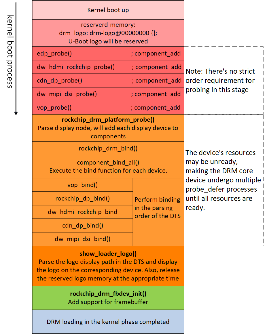
It should be noted that the DRM driver is a combination of drivers for a series of display-related modules. It includes dependent modules on the display path such as backlight, panel, rgb, lvds, dsi, edp, lvds, hdmi, vop, etc. Only when these mutually-dependent modules are all loaded can the entire drm system start successfully.
Due to these complex dependency relationships, during the initialization of the drm system, a certain resource may not be ready temporarily, resulting in a certain module not being able to be loaded smoothly. To solve this problem, the drm driver utilizes the deferred probe mechanism in the Linux driver. When it is found that a dependent resource is not ready, the driver returns - EPROBE_DEFER(-517) and then exits. The Linux kernel will try to load this driver again later until the dependent resource is ready and the driver is loaded successfully.
[1.747190] rockchip-drm display-subsystem: bound fdd90000.vop (ops vop2_component_ops)
[1.747877] dwhdmi-rockchip fde80000.hdmi: registered ddc I2C bus driver
[1.748022] rockchip-drm display-subsystem: bound fde80000.hdmi (ops dw_hdmi_rockchip_ops)
[1.748676] dwhdmi-rockchip fdea0000.hdmi: registered ddc I2C bus driver
[1.748807] rockchip-drm display-subsystem: bound fdea0000.hdmi (ops dw_hdmi_rockchip_ops)
[1.748840] dw-mipi-dsi2 : [drm:dw_mipi_dsi2_bind] *ERROR* Failed to find panel or bridge: -517
[1.755174] panel-simple-dsi fde20000.dsi.0: failed to get power regulator: -517
[1.759296] brd: module loaded
[1.764374] loop: module loaded
[1.764528] zram: Added device: zram0
[1.764698] system_heap: orders[0] = 6
[2.248871] imx415 5-001a: supply dovdd not found, using dummy regulator
[2.416673] rockchip-drm display-subsystem: bound fdd90000.vop (ops vop2_component_ops)
[2.418711] dwhdmi-rockchip fde80000.hdmi: registered ddc I2C bus driver
[2.420336] rockchip-drm display-subsystem: bound fde80000.hdmi (ops dw_hdmi_rockchip_ops)
[2.421725] dwhdmi-rockchip fdea0000.hdmi: registered ddc I2C bus driver
[2.422291] rockchip-drm display-subsystem: bound fdea0000.hdmi (ops dw_hdmi_rockchip_ops)
[2.422318] dw-mipi-dsi2 : [drm:dw_mipi_dsi2_bind] *ERROR* Failed to find panel or bridge: -517
[2.433888] input: adc-keys as /devices/platform/adc-keys/input/input3
[2.466237] rockchip-drm display-subsystem: bound fdd90000.vop (ops vop2_component_ops)
[2.468705] dwhdmi-rockchip fde80000.hdmi: registered ddc I2C bus driver
[2.469751] rockchip-drm display-subsystem: bound fde80000.hnd fde20000.dsi (ops dw_mipi_dsi2_ops)
[2.472282] rockchip-drm display-subsystem: bound fde50000.dp (ops dw_dp_component_ops)
[2.472319] rockchip-drm display-subsystem: bound fde60000.dp (ops dw_dp_component_ops)
[2.531892] rockchip-drm display-subsystem: [drm] fb0: rockchipdrmfb frame buffer device
[2.532850] [drm] Initialized rockchip 3.0.0 20140818 for display-subsystem on minor 0
From the above log, we can see that in the 6th and 18th lines, the mipi dsi driver returns -EPROBE_DEFER and exits because it cannot find the panel or bridge, a dependent resource. Until the 23rd line, the dsi driver successfully binds after obtaining the dependent resource, and finally, we see the standard log indicating that the entire drm driver is loaded.
[2.532850] [drm] Initialized rockchip 3.0.0 20140818 for display-subsystem on minor 0
3.2.4 DTS Configuration
3.2.4.1 Basic Configuration
On an SOC, there may be multiple VOP, HDMI, eDP, DP, MIPI, and Panel modules. According to the specific product definition, a product may only need to use some of these modules to form the display path. Which modules are specifically used and how these modules are connected are configured through dts.
In the core dtsi of each SoC that supports the drm display function, there will be the following display_subsystem node:
display_subsystem: display-subsystem {
    compatible = "rockchip,display-subsystem";
    memory-region = <&drm_logo>, <&drm_cubic_lut>;
    memory-region-names = "drm-logo", "drm-cubic-lut";
    ports = <&vop_out>;
    devfreq = <&dmc>;

    route {
         route_dsi0: route-dsi0 {
              status = "disabled";
              logo,uboot = "logo.bmp";
              logo,kernel = "logo_kernel.bmp";
              logo,mode = "center";
              charge_logo,mode = "center";
              connect = <&vp0_out_dsi0>;
         };
         route_dsi1: route-dsi1 {
              status = "disabled";
              logo,uboot = "logo.bmp";
              logo,kernel = "logo_kernel.bmp";
              logo,mode = "center";
              charge_logo,mode = "center";
              connect = <&vp0_out_dsi1>;
         };
         route_edp: route-edp {
              status = "disabled";
              logo,uboot = "logo.bmp";
              logo,kernel = "logo_kernel.bmp";
              logo,mode = "center";
              charge_logo,mode = "center";
              connect = <&vp0_out_edp>;
         };
         route_hdmi: route-hdmi {
              status = "disabled";
              logo,uboot = "logo.bmp";
              logo,kernel = "logo_kernel.bmp";
              logo,mode = "center";
              charge_logo,mode = "center";
              connect = <&vp1_out_hdmi>;
         };
         route_lvds: route-lvds {
              status = "disabled";
              logo,uboot = "logo.bmp";
              logo,kernel = "logo_kernel.bmp";
              logo,mode = "center";
              charge_logo,mode = "center";
              connect = <&vp1_out_lvds>;
         };
         route_rgb: route-rgb {
              status = "disabled";
              logo,uboot = "logo.bmp";
              logo,kernel = "logo_kernel.bmp";
              logo,mode = "center";
              charge_logo,mode = "center";
              connect = <&vp2_out_rgb>;
         };
    };
};
This node controls the loading of the rockchip_drm_drv.c driver.
The memory-region controls the allocation and transfer of the logo display buffer. This attribute will be dynamically modified in U- Boot during system startup and then passed to the kernel.
The route_xxx nodes control whether the startup logo function of each interface is enabled. By default , it is in the disabled state.
Taking the route_rgb as an example, the functions of related attributes are explained as follows:
route_rgb: route-rgb {
  status = "disabled";
     logo,uboot = "logo.bmp";
     logo,kernel = "logo_kernel.bmp";
     logo,mode = "center";
     charge_logo,mode = "center";
     connect = <&vp2_out_rgb>;
};
logo,uboot and logo,kernel describe the names of the logo pictures in the U-Boot and Kernel stages, which need to match the actual picture resources.
logo,mode and charege_logo,mode control the display mode of the logo picture, with two modes: center and fullscreen .
connect describes which Video Port of the VOP (VOP2.0 architecture) or which VOP (VOP1.0 architecture) this display interface is connected to. It is generally configured according to the actual usage situation.
Most of the attributes of the display_subsystem node do not need to be modified. Generally, only the corresponding logo nodes need to be enabled or disabled according to the actual product requirements.
The vop node:
vop: vop@fe040000 {
  compatible = "rockchip,rk3568-vop";
  reg = <0x0 0xfe040000 0x0 0x3000>, <0x0 0xfe044000 0x0 0x1000>;
  reg-names = "regs", "gamma_lut";
  rockchip,grf = <&grf>;
  interrupts = <GIC_SPI 148 IRQ_TYPE_LEVEL_HIGH>;
  clocks = <&cru ACLK_VOP>, <&cru HCLK_VOP>, <&cru DCLK_VOP0>, <&cru DCLK_VOP1>, <&cru DCLK_VOP2>;
  clock-names = "aclk_vop", "hclk_vop", "dclk_vp0", "dclk_vp1", "dclk_vp2";
  iommus = <&vop_mmu>;
  power-domains = <&power RK3568_PD_VO>;
  status = "disabled";
  vop_out: ports {
     ......
     vp0: port@0 {
       ......
       vp0_out_dsi0: endpoint@0 {
         reg = <0>;
         remote-endpoint = <&dsi0_in_vp0>;
       };
       vp0_out_dsi1: endpoint@1 {
         reg = <1>;
         remote-endpoint = <&dsi1_in_vp0>;
       };

       vp0_out_edp: endpoint@2 {
         reg = <2>;
         remote-endpoint = <&edp_in_vp0>;
       };
       vp0_out_hdmi: endpoint@3 {
         reg = <3>;
         remote-endpoint = <&hdmi_in_vp0>;
       };
     };
     vp1: port@1 {
       ......
       vp1_out_dsi0: endpoint@0 {
         reg = <0>;
         remote-endpoint = <&dsi0_in_vp1>;
       };

       vp1_out_dsi1: endpoint@1 {
         reg = <1>;
         remote-endpoint = <&dsi1_in_vp1>;
       };

       vp1_out_edp: endpoint@2 {
         reg = <2>;
         remote-endpoint = <&edp_in_vp1>;
       };
       vp1_out_hdmi: endpoint@3 {
         reg = <3>;
         remote-endpoint = <&hdmi_in_vp1>;
       };

       vp1_out_lvds: endpoint@4 {
         reg = <4>;
         remote-endpoint = <&lvds_in_vp1>;
       };
     };
     vp2: port@2 {
       ......
       vp2_out_lvds: endpoint@0 {
         reg = <0>;
         remote-endpoint = <&lvds_in_vp2>;
       };
       vp2_out_rgb: endpoint@1 {
         reg = <1>;
         remote-endpoint = <&rgb_in_vp2>;
       };
     };
  };
};
This node describes the VOP hardware resources and controls the loading of the vop driver rockchip_drm_vop.c/rockchip_drm_vop2.c . It describes the following display path connection relationships:
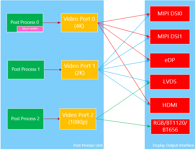
The vop_out: ports node describes the output channels of the VOP. vp0/1/2 correspond to the three independent output paths of Video Port0/1/2 on the VOP.
The endpoint nodes under vp0/1/2 : port describe the connection relationship between the VP and the display interface. Taking the above dts description as an example, the vp0 node has four nodes: vp0_out_dsi0 , vp0_out_dsi1 , vp0_out_edp , and vp0_out_hdmi , indicating that vp0 can be connected to four display interfaces: dsi0, dsi1, edp, and hdmi.
Each endpoint forms a connection path with the corresponding display interface through the remote-endpoint attribute. For example, the connection with the hdmi display interface:
hdmi: hdmi@fe0a0000 {
  compatible = "rockchip,rk3568-dw-hdmi";
  ......
  status = "disabled";

  ports {
     ......
     port@0 {
       reg = <0>;
       ......
       hdmi_in_vp0: endpoint@0 {
         reg = <0>;
         remote-endpoint = <&vp0_out_hdmi>;
         status = "disabled";
       };
       hdmi_in_vp1: endpoint@1 {
         reg = <1>;
         remote-endpoint = <&vp1_out_hdmi>;
         status = "disabled";
       };
     };
  };
};
Combined with the above dts description, we know that on rk3568, hdmi can be connected to vp0 and vp1 of vop.
It should be noted that a display interface can only be connected to one vp at the same time. Therefore, in the specific board-level configuration, the used paths need to be enabled in the dts, and the unused paths should be set to the disabled state.
For example, in a certain product, if it is desired to connect HDMI to vp0, the following settings need to be made in the dts:
&hdmi {
     status = "okay";
};

&hdmi_in_vp0 {
     status = "okay";
};
&hdmi_in_vp1 {
     status = "disabled";
};

&route_hdmi {
     status = "okay";
     connect = <&vp0_out_hdmi>;
};
3.2.4.2 Specify Layer Allocation Strategy
VOP2 adopts a unified display architecture. The independent Video Ports share all the layer resources inside the VOP, and these layers need to be used exclusively, that is, a certain layer can only be occupied by one Video Port at the same time.
In order to make full and rational use of all layer resources, a default layer allocation strategy is generated in U-Boot according to the interface types and quantities configured in the current product dts. If some products do not enable the U-Boot logo display or have special requirements for layer usage, they can refer to the following writing method to specify the layer allocation strategy in the dts according to their needs:
rockchip,plane-mask : Specify the layer ID mask set allocated to this VP. The layer IDs are defined in dt- bindings/display/rockchip_vop.h .
rockchip,primary-plane : Specify the primary layer. The primary layer of the current VP must be one of the rockchip,plane-mask. We generally choose the Smart or Esmart layer.
The basic principle of layer allocation is to evenly distribute all layers (rk3568 has 6 layers, and rk3588 has 8 layers) to each used VP. Unused VPs are generally not allocated layers. Since different types of layers (Cluster, Esmart, Smart) inside the VOP have different performances and limitations, it is generally recommended to evenly allocate various types of layers.
The following is a typical layer allocation reference on RK3568. The RK3568 VOP has a total of 6 layers (2 Cluster + 2 Esmart + 2 Smart). This configuration supports three-screen different-display. Generally, we try to allocate more than three layers to the VP corresponding to the screen with the most usage scenarios (main screen) (in this application case, it is VP1), and other interfaces are allocated no less than two layers.
#include <dt-bindings/display/rockchip_vop.h> // Layer ID definition header file

&vp0 {
  rockchip,plane-mask = <(1 << ROCKCHIP_VOP2_CLUSTER1 | 1 << ROCKCHIP_VOP2_SMART1)>;
  rockchip,primary-plane = <ROCKCHIP_VOP2_SMART1>;
};

&vp1 {
  rockchip,plane-mask = <(1 << ROCKCHIP_VOP2_CLUSTER0 | 1 << ROCKCHIP_VOP2_ESMART0 | 1 <<
ROCKCHIP_VOP2_SMART0)>;
  rockchip,primary-plane = <ROCKCHIP_VOP2_SMART0>;
};
&vp2 {
  rockchip,plane-mask = <(1 << ROCKCHIP_VOP2_ESMART1)>;
  rockchip,primary-plane = <ROCKCHIP_VOP2_ESMART1>;
};
After the configuration takes effect, the corresponding plane mask parsing information can be seen from the startup logs of U- Boot and Linux kernel when the system starts.
Rockchip UBOOT DRM driver version: v1.0.1
VOP have 3 active VP
vp0 have layer nr:2[1 5 ], primary plane: 5
vp1 have layer nr:3[0 2 4 ], primary plane: 4
vp2 have layer nr:1[3 ], primary plane: 3
Using display timing dts
dsi@fe060000: detailed mode clock 132000 kHz, flags[8000000a]
  H: 1080 1095 1097 1127
  V: 1920 1935 1937 1952
bus_format: 100e
VOP update mode to: 1080x1920p0, type: MIPI0 for VP1
VOP VP1 enable Smart0[654x270->654x270@213x825] fmt[2] addr[0x7df04000]
final DSI-Link bandwidth: 876 Mbps x 4
disp info 0, type:11, id:0
xfer: num: 2, addr: 0x50
xfer: num: 2, addr: 0x50
[2.314574] panel-simple-dsi fe060000.dsi.0: Specify missing connector_type
[2.315764] rockchip-vop2 : [drm:vop2_bind] vp0 assign plane mask: 0x22, primary plane phy id: 5
[2.315807] rockchip-vop2 : [drm:vop2_bind] vp1 assign plane mask: 0x15, primary plane phy id: 4
[2.315828] rockchip-vop2 : [drm:vop2_bind] vp2 assign plane mask: 0x8, primary plane phy id: 3
[2.316713] rockchip-drm display-subsystem: bound fe040000.vop (ops vop2_component_ops)
[2.317966] rockchip-drm display-subsystem: bound fe0c0000.edp (ops rockchip_dp_component_ops)
[2.318378] dwhdmi-rockchip : Detected HDMI TX controller v2.11a with HDCP (DWC HDMI 2.0 TX PHY)
[2.319625] dwhdmi-rockchip : registered DesignWare HDMI I2C bus driver
[2.321857] rockchip-drm display-subsystem: bound fe0a0000.hdmi (ops dw_hdmi_rockchip_ops)
[2.322069] rockchip-drm display-subsystem: bound fe060000.dsi (ops dw_mipi_dsi_rockchip_ops)
3.2.4.2.1 RK3566 Layer Allocation Strategy
In the RK3566 IC implementation, there is a difference between the main layer and the mirror layer, that is, the mirror layer Cluster1 can only fetch data from the address corresponding to the main layer Cluster0. Similarly, Esmart1/Smart1 can only fetch data from the address corresponding to Esmart0/Smart0. Therefore, we need to ensure that the main layer is used first. In the U- Boot display driver of normal products, the plane-mask attribute will be set according to the type of display interface. If some products do not enable the U-Boot logo display, they can be configured in the dts according to the following rules:
1. For single-screen display, the following configuration can be used:
#include <dt-bindings/display/rockchip_vop.h> // Layer ID definition header file

&vpx { // x depends on the used vp id, such as vp0
  rockchip,plane-mask = <(1 << ROCKCHIP_VOP2_CLUSTER0 | 1 << ROCKCHIP_VOP2_ESMART0 | 1 <<
ROCKCHIP_VOP2_SMART0 | 1 << ROCKCHIP_VOP2_CLUSTER1 | 1 << ROCKCHIP_VOP2_ESMART1 | 1 << ROCKCHIP_VOP2_SMART1)>;
  rockchip,primary-plane = <ROCKCHIP_VOP2_SMART0>;
};
2. For two-screen display [RK3566 currently only Android products support dual-screen display, and the refresh rates of the two screens are required to be the same], we let the device that does not support hot-plugging (that is, the display path that is always connected) use the main layer, and the other path uses the mirror layer:
#include <dt-bindings/display/rockchip_vop.h> // Layer ID definition header file

&vpx { // x depends on the used vp id, such as vp0
  rockchip,plane-mask = <(1 << ROCKCHIP_VOP2_CLUSTER0 | 1 << ROCKCHIP_VOP2_ESMART0 | 1 <<
ROCKCHIP_VOP2_SMART0)>;
  rockchip,primary-plane = <ROCKCHIP_VOP2_SMART0>;
}; // Single-screen or non-hot-plugging main display device in dual-screen display uses the main layer
&vpx { // x depends on the used vp id, such as vp1
  rockchip,plane-mask = <(1 << ROCKCHIP_VOP2_CLUSTER1 | 1 << ROCKCHIP_VOP2_ESMART1 | 1 <<
ROCKCHIP_VOP2_SMART1)>;
  rockchip,primary-plane = <ROCKCHIP_VOP2_SMART1>;
};
3.2.4.3 Set a Certain Layer as the Mouse Layer
If an application uses the Atomic display interface, it does not need to distinguish the types of layers (primary, overlay, cursor). It only needs to use any available layer for various types of displays according to the formats supported by the layers.
However, in the Linux system (non-Android), there are still some applications that use the legacy API. These APIs care about the layer types. For example, the primary layer is used to display the desktop background, the overlay layer is used to play videos, and the cursor layer is used to display the mouse.
The Rockchip drm driver only registers the primary layer and the overlay layer by default and does not register the cursor layer. If some special Linux systems want to use the cursor layer, they can set the cursor-win-id attribute under the corresponding vp node in the dts to allocate a cursor layer for the crtc corresponding to this VP.
&vp0 {
  cursor-win-id = <ROCKCHIP_VOP2_CLUSTER0>;
};
Because the Cluster layers of RK3566/RK3568 only support the AFBC format (do not support any non-AFBC compressed RGB/YUV formats. It is illegal to send non-AFBC format display data to the Cluster layer in any scenario), if the Cluster layer is specified as the mouse layer in the Linux system (buildroot, Debian, etc., non-Android systems), it needs to be used in conjunction with the libdrm-cursor library provided by the Linux SDK. This library can perform corresponding data format conversion according to the characteristics of specific layers. For specific details, please refer to 《Rockchip_Developer_Guide_Debian_CN.pdf》.
3.2.4.3.1 Connection Relationship between Layers and VPs
For RK356X/RK3588/RK3562, each layer is connected to any VP, and there are no special configuration requirements. For RK3528 and RK3576, not every layer can be connected to any VP. Therefore, when configuring the cursor layer of a VP, a layer that can be connected to the current VP needs to be selected. The following are the connection relationships between layers and VPs on different platforms:
1. RK3528
| VP | Layers |
|---|---|
| VP0 | Cluster0, Esmart0, Esmart1, Esmart2 |
| VP1 | Esmart2, Esmart3 |
2. RK3576
| VP | Layers |
|---|---|
| VP0 | Cluster0, Cluster1, Esmart0, Esmart2 |
| VP1 | Cluster0, Cluster1, Esmart1, Esmart3 |
| VP2 | Esmart0, Esmart1, Esmart2, Esmart3 |
3.2.4.4 esmart Layer Segmentation
In RK3528 and RK3576, several esmart layers share the linebuffer, and it can be segmented according to the product form to support different numbers of layers and performance:
3.2.4.4.1 RK3528 esmart Layer Segmentation
On the RK3528 platform, esmart0/1/2/3 share the linebuffer. The default configuration is: VOP3_ESMART_4K_2K_2K_MODE, that is, in addition to the fixed cluster layer, esmart0[4k], esmart2[2k], and esmart3[2k] are also registered. It can also be modified in the dts according to product requirements. For example, to change it to two 4k-supported layers, the following configuration can be used:
&vop {
  esmart_lb_mode = /bits/ 8 <1>;
};
Configuration description:
| esmart_lb_mode | val | Number and Performance of Layers |
|---|---|---|
| VOP3_ESMART_4K_4K_MODE | 1 | Register cluster[4k], esmart0[4k], esmart2[4k] |
| VOP3_ESMART_4K_2K_2K_MODE | 2 | Register cluster[4k], esmart0[4k], esmart2[2k], esmart3[2k] |
| VOP3_ESMART_2K_2K_2K_2K_MODE | 3 | Register cluster[4k], esmart0[2k], esmart1[2k], esmart2[2k], esmart3[2k] |
3.2.4.4.2 RK3576 esmart Layer Segmentation
On the RK3576 platform, in addition to the fixed configurations of Cluster0/1[4k] and esmart0/1[4k], esmart2[2k] and esmart3[2k] also share the linebuffer design. The default configuration is two 2k layers. To change it to one 4k-supported layer, the following configuration can be used:
&vop {
  esmart_lb_mode = /bits/ 8 <4>;
};
Configuration description:
| esmart_lb_mode | val | Number and Performance of Layers |
|---|---|---|
| VOP3_ESMART_4K_4K_4K_MODE | 4 | Register cluster0[4k], cluster1[4k], esmart0[4k], esmart1[4k], esmart2[4k] |
| VOP3_ESMART_4K_4K_2K_2K_MODE | 5 | Register cluster0[4k], cluster1[4k], esmart0[4k], esmart1[4k], esmart2[2k], esmart3[2k] |
3.2.4.5 Prohibit Layer Migration
RK3568 and RK3588 do not support the free migration of layers between VPs/CRTCs during runtime. Therefore, on most Linux (non-Android) systems, layers should be configured to be exclusively occupied by a fixed CRTC and not allowed to be dynamically migrated between CRTCs. That is, it is necessary to ensure that the disable-win-move attribute is added under the vop node in the dts.
&vop {
     disable-win-move;
}
After the system starts, the possible crtcs attribute of the layer can be viewed through modetest . The possible crtcs attribute value of each layer should only have one bit set, otherwise it does not meet the expectations.
3.2.5 Color Gamut-related Configuration Description
The DRM driver framework of the Linux 6.1 kernel added the standard definition of color gamut. The original DRM driver borrowed the color gamut definition of V4L2, which is not very formal, and the definition of V4L2 is not easy to understand. Therefore, in the Linux 6.1 kernel, the color gamut definition of the layer Plane was switched to the DRM standard definition. The following is the color gamut configuration description of several kernel versions of the RK platform based on the DRM driver framework:
3.2.5.1 Plane Color Gamut Configuration Description
1. Kernel versions before Linux 6.1
Use the RK private attribute: COLOR_SPACE
| Configuration Value | Color Gamut |
Description |
|---|---|---|
| V4L2_COLORSPACE_SMPTE170M / V4L2_COLORSPACE_470_SYSTEM_M / V4L2_COLORSPACE_470_SYSTEM_BG |
BT.601L | V4L2 definition |
| V4L2_COLORSPACE_REC709 / V4L2_COLORSPACE_SMPTE240M / V4L2_COLORSPACE_DEFAULT |
BT.709L | V4L2 definition |
| V4L2_COLORSPACE_JPEG | BT.601F | V4L2 definition |
| V4L2_COLORSPACE_BT2020 | BT.2020L | V4L2 definition |
| V4L2_COLORSPACE_BT709F | BT.709F | RK private definition |
| V4L2_COLORSPACE_BT2020F | BT.2020F | RK private definition |
2. Linux 6.1 and later kernel versions
Use two attributes defined by the DRM framework: COLOR_ENCODING and COLOR_RANGE
COLOR_ENCODING
| Configuration Value | Color Gamut | Description |
|---|---|---|
| DRM_COLOR_YCBCR_BT601 | BT.601 | DRM definition |
| DRM_COLOR_YCBCR_BT709 | BT.709 | DRM definition |
| DRM_COLOR_YCBCR_BT2020 | BT.2020 | DRM definition |
COLOR_RANGE
| Configuration Value | range | Description |
|---|---|---|
| DRM_COLOR_YCBCR_FULL_RANGE | Full | DRM definition |
| DRM_COLOR_YCBCR_LIMITED_RANGE | Limit | DRM definition |
3.2.5.2 Connector Color Gamut Configuration Description
1. Kernel versions before Linux 5.10
Color gamut uses the RK private attribute: hdmi_output_colorimetry
| Attribute Value | Color Gamut | Description |
|---|---|---|
| HDMI_COLORIMETRY_NONE | Default | RK private definition |
| RK_HDMI_COLORIMETRY_BT2020 | BT.2020 | RK private definition |
range uses the RK private definition: hdmi_quant_range
| Configuration Value | range | Description |
|---|---|---|
| HDMI_QUANTIZATION_RANGE_DEFAULT | Default | RK private definition |
| HDMI_QUANTIZATION_RANGE_LIMITED | Limit | RK private definition |
| HDMI_QUANTIZATION_RANGE_FULL | Full | RK private definition |
2. Linux 5.10 kernel version
Color gamut uses the standard attribute defined by DRM: Colorspace
| Configuration Value | Color Gamut | Description |
|---|---|---|
| Default = 0 | Default | DRM definition |
| DRM_MODE_COLORIMETRY_SMPTE_170M_YCC | SMPTE_170M_YCC | DRM definition |
| DRM_MODE_COLORIMETRY_BT709_YCC | BT709_YCC | DRM definition |
| DRM_MODE_COLORIMETRY_XVYCC_601 | XVYCC_601 | DRM definition |
| DRM_MODE_COLORIMETRY_XVYCC_709 | XVYCC_709 | DRM definition |
| DRM_MODE_COLORIMETRY_SYCC_601 | SYCC_601 | DRM definition |
| DRM_MODE_COLORIMETRY_OPYCC_601 | opYCC_601 | DRM definition |
| DRM_MODE_COLORIMETRY_OPRGB | opRGB | DRM definition |
| DRM_MODE_COLORIMETRY_BT2020_CYCC | BT2020_CYCC | DRM definition |
| DRM_MODE_COLORIMETRY_BT2020_RGB | BT2020_RGB | DRM definition |
| DRM_MODE_COLORIMETRY_BT2020_YCC | BT2020_YCC | DRM definition |
| DRM_MODE_COLORIMETRY_DCI_P3_RGB_D65 | P3_RGB_D65 | DRM definition |
| DRM_MODE_COLORIMETRY_DCI_P3_RGB_THEATER | P3_RGB_Theater | DRM definition |
Currently, the DRM HDMI driver only differentiates several color gamuts of BT2020. If the application does not specify the BT2020 color gamut, the driver will specify the color gamut of the HDMI output according to different resolutions.
range uses the RK private definition: hdmi_quant_range
| Configuration Value | range | Description |
|---|---|---|
| HDMI_QUANTIZATION_RANGE_DEFAULT | Default | RK private definition |
| HDMI_QUANTIZATION_RANGE_LIMITED | Limit | RK private definition |
| HDMI_QUANTIZATION_RANGE_FULL | Full | RK private definition |
3. Linux 6.1 kernel version
The color gamut is the same as that of the Linux 5.10 kernel version, using the standard attribute defined by DRM: Colorspace;
range uses the RK private attribute, and the attribute name is changed from “hdmi_quant_range” to “quant_range”, mainly for reuse with DP:
| Configuration Value | range | Description |
|---|---|---|
| HDMI_QUANTIZATION_RANGE_DEFAULT | Default | RK private definition |
| HDMI_QUANTIZATION_RANGE_LIMITED | Limit | RK private definition |
| HDMI_QUANTIZATION_RANGE_FULL | Full | RK private definition |
3.2.5.3 Other Instructions
1. The configuration of DP is basically the same as that of HDMI, and some functions may still be missing and will be improved in the future;
2. Different kernel versions can be judged using the Libdrm standard interface: drmGetVersion().
| Kernel Version | Version Number |
|---|---|
| Linux 4.4 | 1.0 |
| Linux 4.19 | 2.0 |
| Linux 5.10 | 3.0 |
| Linux 6.1 | 4.0 |
3. Currently, the Plane attributes defined by the DRM framework only consider data in the YUV format, and the color gamut of the RGB format is not defined. Therefore, for the RGB format, we temporarily use the color gamut definition of YUV, that is:
For ordinary UI (SRGB + Full Range) configuration attributes: COLOR_ENCODING = DRM_COLOR_YCBCR_BT709, COLOR_RANGE = DRM_COLOR_YCBCR_FULL_RANGE;
4. Display feature
4.1 Basic VOP Features of Each Platform
| SOC | VOP-version | 8K | 4K | MMU | i-MODE | A/IFBDC | MULTIAREA | BCSH | gamma | 3D-LUT | POST-SCALE | X-mirror |
|---|---|---|---|---|---|---|---|---|---|---|---|---|
| RK3066/PX2 | V1.0 | × | × | × | × | × | × | × | √ | × | × | × |
| RK3188/PX3 | V1.0 | × | × | × | × | × | × | × | √ | × | × | × |
| RK3126/RK3126C | V1.0 | × | × | √ | × | × | × | √ | √ | × | × | × |
| RK3128/PX3SE | V1.0 | × | × | √ | √ | × | × | √ | √ | × | × | × |
| RK3036 | V1.0 | × | × | √ | √ | × | × | √ | √ | × | × | × |
| RK322X/RK312XH | V1.0 | × | √ | √ | √ | × | × | √ | × | × | √ | × |
| RK322XH/RK332X | V1.0 | × | √ | √ | √ | × | × | √ | × | × | √ | × |
| SOFIA 3GR | V1.0 | × | × | √ | × | × | × | √ | √ | × | × | × |
| RV1108 | V1.0 | × | × | × | √ | × | × | √ | √ | × | × | × |
| RK3288 | V1.0 | × | √ | √ | × | × | √ | √ | √ | × | √ | × |
| RK3368/PX5 | V1.0 | × | √ | √ | × | √ | √ | √ | √ | × | √ | × |
| RK3399 | V1.0 | × | √ | √ | √ | √ | √ | √ | √ | × | √ | × |
| RK3326/PX30 | V1.0 | × | × | √ | √ | √ | √ | √ | √ | × | × | × |
| RK3308 | V1.0 | × | × | × | × | × | × | √ | √ | × | × | × |
| RK1808 | V1.0 | × | × | √ | × | × | × | √ | √ | × | × | × |
| RV1109/RV1126 | V1.0 | × | × | √ | × | × | × | √ | √ | × | × | × |
| RV1103/RV1106 | V1.0 | × | × | × | √ | × | × | √ | √ | × | × | × |
| RK356X | V2.0 | × | √ | √ | √ | √ | √ | √ | √ | √ | √ | √ |
| RK3588 | V2.0 | √ | √ | √ | √ | √ | √ | √ | √ | √ | × | √ |
| RK3528 | V3.0 | × | √ | √ | √ | √ | √ | √ | √ | √ | √ | √ |
| RK3562 | V3.0 | × | × | √ | √ | × | √ | √ | √ | √ | √ | √ |
| RK3576 | V3.0 | × | √ | √ | √ | √ | √ | √ | √ | √ | √ | √ |
| RK3506 | V1.0 | × | × | × | √ | × | × | √ | √ | × | × | × |
| RV1126B | V1.0 | × | × | √ | √ | × | × | √ | √ | × | × | × |
4.2 Maximum Output Resolution and Protocol Standards of Display Interfaces for Each Platform
| Platform | Display Interface |
Maximum Output Resolution | Protocol Standard |
|---|---|---|---|
| RK3036 | HDMI | 1920x1080@60hz | Supports HDMI 1.4a protocol standard |
| RK3036 | CVBS | 720x480i@60hz/720x576i@50hz | Supports NTSC/PAL standard output |
| RK312X/PX3SE | RGB | 1280x800@60hz | Supports RGB666/sRGB888 |
| RK312X/PX3SE | LVDS | 1280x800@60hz | Supports VESA and JEIDA LVDS data formats |
| RK312X/PX3SE | MIPI | 1920x1080@60hz | Supports DSI v1.0, DCS v1.0, DPHY v1.0 protocol standards |
| RK312X/PX3SE | HDMI | 1920x1080@60hz | Supports HDMI 1.4a protocol standard |
| RK312X/PX3SE | CVBS | 720x480i@60hz/720x576i@50hz | Supports NTSC/PAL standard output |
| RK322X/RK312XH | HDMI | 4096x2160@60hz | Supports HDMI 1.4a protocol standard |
| RK322X/RK312XH | CVBS | 720x480i@60hz/720x576i@50hz | Supports NTSC/PAL standard output |
| RK3288 | RGB | 1920x1080@60hz | Supports GB888/RGB666/sRGB888 |
| RK3288 | LVDS | Single-channel 1280x800@60hz Dual-channel:1920x1080@60hz |
Supports VESA and JEIDA LVDS data formats |
| RK3288 | eDP | 2560x1600@60hz | Supports DP1.2a and eDP1.3 protocol standards |
| RK3288 | MIPI | Single- channel1920x1080@60hz Dual-channel:2560x1600@60hz |
Supports DSI v1.1, DCS v1.1, DPHY v1.1 protocol standards |
| RK3288 | HDMI | VOP BIG: 3840x2160@60hz VOP LIT: 1920x1080@60hz |
Supports HDMI 1.4a and 2.0 protocol standards |
| RK3308 | RGB | 1280x800@60hz | Supports RGB888/RGB666/sRGB888/MCU |
| RK1808 | RGB | 1280x800@60hz | Supports RGB888/RGB666/sRGB888/MCU |
| RK1808 | MIPI | 1280X800@60hz | Supports DSI v1.0, DCS v1.0, DPHY v1.0 protocol standards |
| RK322XH/RK332X | HDMI | 3840x2160@60hz | Supports HDMI 1.4a and 2.0 protocol standards |
| RK322XH/RK332X | CVBS | 720x480i@60hz/720x576i@50hz | Supports NTSC/PAL standard output |
| RK3326/px30 | RGB | 1280x800@60hz | Supports RGB888/RGB666/sRGB888/MCU |
| RK3326/px30 | LVDS | 1280x800@60hz | Supports VESA and JEIDA LVDS data formats |
| RK3326/px30 | MIPI | 1920x1080@60hz | Supports DSI v1.0, DCS v1.0, DPHY v1.0 protocol standards |
| RK3368/PX5 | RGB | 1280x800@60hz | Supports RGB888/RGB666/sRGB888/MCU |
| RK3368/PX5 | LVDS | 1280x800@60hz | Supports VESA and JEIDA LVDS data formats |
| RK3368/PX5 | MIPI | 1920x1080@60hz | Supports DSI v1.0, DCS v1.0, DPHY v1.0 protocol standards |
| RK3368/PX5 | eDP | 2560x1600@60hz | Supports DP1.2a and eDP1.3 protocol standards |
| RK3368/PX5 | HDMI | 4096x2160@60hz | Supports HDMI 1.4a and 2.0 protocol standards |
| RK3399 | MIPI | Single-channel:1280x800@60hz Dual-channel:2560x1600@60hz |
Supports DSI v1.1, DCS v1.1, DPHY v1.1 protocol standards |
| RK3399 | eDP | 2560x1600@60hz | Supports DP1.2a and eDP1.3 protocol standards |
| RK3399 | HDMI | VOP BIG: 4096x2160@60hz VOP LIT: 2560x1600@60hz |
Supports HDMI 1.4a and 2.0a protocol standards |
| RK3399 | DP | VOP BIG: 3840x2160@60hz VOP LIT: 2560x1600@60hz |
Supports DP 1.2 protocol standard |
| RV1109/RV1126 | RGB | 1920x1080@60hz | Supports RGB888/RGB666/sRGB888/MCU/BT.1120 |
| RV1109/RV1126 | MIPI | 1920x1080@60hz | Supports DSI v1.1, DCS v1.1, DPHY v1.2 protocol standards |
| RK356X | RGB | 1920x1080@60hz | Supports RGB888/RGB666/BT.656/BT.1120 |
| RK356X | MIPI | Single- channel:1920x1080@60hz Dual-channel:2560x1600@60hz |
Supports DSI v1.1, DCS v1.1, DPHY v1.1 protocol standards |
| RK356X | eDP | 2560x1600@60hz | Supports DP 1.2a and eDP 1.3 protocol standards |
| RK356X | HDMI | 4096x2160@60hz | Supports HDMI 1.4a and 2.0a protocol standards |
| RK3588 | RGB | 1920x1080@60hz | Supports BT.656/BT.1120 |
| RK3588 | MIPI | 3840x2160@60hz | Dual MIPI, supports DSI v1.1, DCS v1.1, DPHY v2.0, CPHY V1.1 protocol standards |
| RK3588 | eDP0 | 3840x2160@60hz | Dual eDP, supports DP1.2a and eDP1.3 protocol standards |
| RK3588 | HDMI | 7680x4320@60hz | Dual HDMI, supports HDMI 2.1 protocol standard |
| RK3588 | DP | 7680x4320@30hz | Dual DP, supports DP1.4 protocol standard |
| RV1103/RV1106 | RGB | 1280x720@60hz | Supports RGB666/RGB565/sRGB888/MCU/BT.656/BT.1120 |
| RK3528 | HDMI | 4096x2160@60hz | Supports HDMI 2.0 protocol standard |
| RK3528 | CVBS | 720x480i@60hz/720x576i@50hz | Supports NTSC/PAL standard output |
| RK3562 | RGB | 1920x1080@60hz | Supports RGB888/RGB666/RGB565/sRGB888/MCU/BT.656/BT.1120 |
| RK3562 | MIPI | 2048x1080@60hz | Supports DSI v1.1, DCS v1.1, DPHY v1.2 protocol standards |
| RK3562 | LVDS | 1280x800@60hz | Supports VESA and JEIDA LVDS data formats |
| RK3576 | HDMI | 4096x2160@120hz | Supports HDMI 2.1 protocol standard |
| RK3576 | DP | 4096x2160@120hz | Supports DP1.4 protocol standard |
| RK3576 | MIPI | 2560x1600@60hz | Supports DSI v1.1, DCS v1.4, DPHY v2.0 protocol standards |
| RK3576 | eDP | 4096x2160@60hz | Supports DP1.2 and eDP1.3 protocol standards |
| RK3576 | RGB | 1920x1080@60hz | Supports RGB888/RGB666/RGB565/sRGB888/MCU/BT.656/BT.1120 |
| RK3506 | RGB | 1280x720@60hz | Supports RGB888/RGB666/RGB565/sRGB888/MCU/BT.656/BT.1120 |
| RK3506 | MIPI | 1280x720@60hz | Supports DSI v1.1, DCS v1.1, DPHY v1.2 protocol standards |
| RV1126B | RGB | 1920x1080@60hz | Supports RGB888/RGB666/RGB565/sRGB888/MCU/BT.656/BT.1120 |
| RV1126B | MIPI | 1920x1080@60hz | Supports DSI v1.1, DCS v1.1, DPHY v1.2 protocol standards |
Note:
- On RK3576/RK3588, the PHYs of eDP and HDMI are combo. That is, on the same product, if HDMI0 is used, eDP0 cannot be used, and the same applies to HDMI1 and eDP1.
4.3 Display Paths on VOP2 Platforms
4.3.1 Connection Relationship between RK3528 VP and Each Display Interface
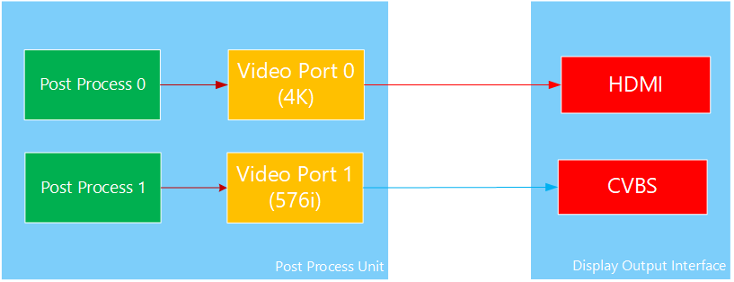
Among them, the 4K resolution of VP0 is 4096x2304, and the 576i resolution of VP1 is 720x576. For more detailed content, please refer to the Display Interface and Video Output Processor chapters of 《Rockchip RK3528 datasheet》.
4.3.2 Connection Relationship between RK3562 VP and Each Display Interface
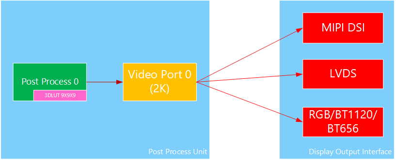
Among them, the 2K resolution of VP0 is 2048x1080. For more detailed content, please refer to the Display Interface and Video Output Processor chapters of 《Rockchip RK3562 datasheet》.
4.3.3 Connection Relationship between RK3568 VP and Each Display Interface
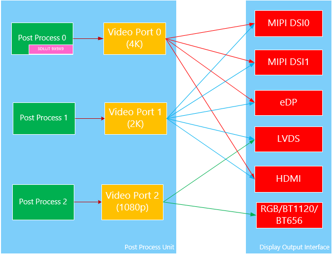
For more detailed content, please refer to the Display Interface and Video Output Processor chapters of 《Rockchip RK3568 datasheet》.
4.3.4 Connection Relationship between RK3576 VP and Each Display Interface
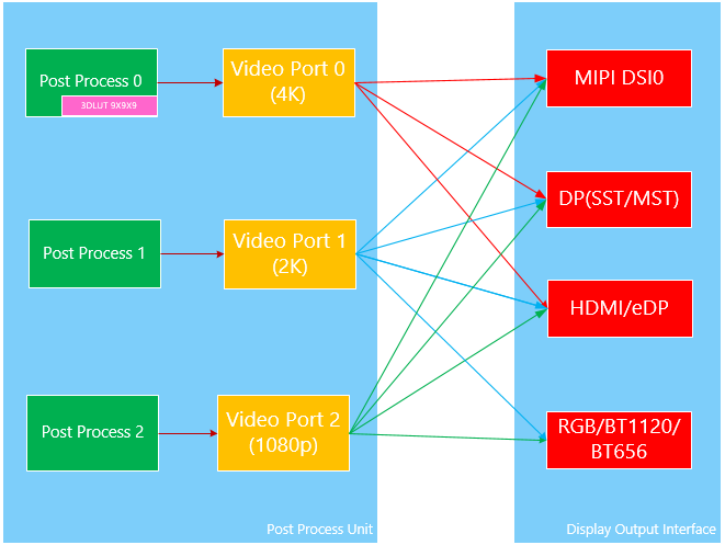
It should be noted that the 2K resolution corresponding to VP1 in the above figure is 2560x1600. For more detailed content, please refer to the Display Interface and Video Output Processor chapters of 《Rockchip RK3576 datasheet》.
4.3.5 Connection Relationship between RK3588 VP and Each Display Interface
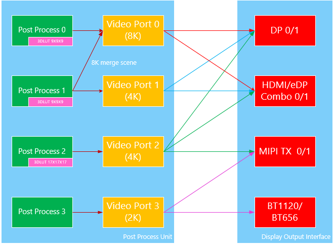
It should be noted that the HDMI and DP of RK3588 support 8K output. However, in the 8K output mode, one display interface needs to occupy both VP0 and VP1 simultaneously. Therefore, if 8K display output is required in the product, attention should be paid not to connect other display interfaces to VP1. For more detailed content, please refer to the Display Interface and Video Output Processor chapters of 《Rockchip RK3588 datasheet》.
Please refer to 《Rockchip RK3588 datasheet》 Display Interface and Video Output Processor .
4.4 Display Specifications of Extended Chips
4.4.1 RK3566
Compared with RK3568, RK3566 only supports dual-screen same-display, and the requirements for the screens are as follows:
The refresh rates of the two screens are required to be the same.
The display directions of the two screens are required to be the same, that is, both are in landscape or portrait mode.
For the use of RK3566 dual-screen display, please refer to the RK3566 Layer Allocation Strategy section.
4.4.2 RK3576s
Compared with RK3576, RK3576s only retains Video Port0, and the RGB/BT.1120/BT.656/MCU display interfaces are unavailable.
4.4.3 RK3588s
Compared with RK3588, RK3588s does not have the HDMI1, DP1, and eDP1 display interfaces.
4.5 VOP Platform DCLK Clock Allocation Strategies
4.5.1 RK3399 VOP DCLK Allocation Strategy
RK3399 has two VOPs, namely VOPB[VOP0] and VOPL[VOP1]. The PLLs that can be used by the two VOPs are VPLL/CPLL. Among them, VPLL is a PLL dedicated to display. Specifically, for the HDMI path, the DCLK of the VOP must be divided from VPLL, which needs to be correctly specified in the DTS. If the DTS configuration is incorrect, the driver will switch the HDMI path to VPLL and perform a resolution switching process. Phenomenally, it is like a process of turning off and then turning on the display. The DTS reference configuration is as follows:
&hdmi_in_vopl {
  status = "disabled";
};

&hdmi_in_vopb {
  status = "okay";
};
&route_hdmi {
  connect = <&vopb_out_hdmi>;
};

&vopb {
  status = "okay";
  assigned-clocks = <&cru DCLK_VOP0_DIV>;
  /* The dclk parent for VOP->HDMI must from VPLL */
  assigned-clock-parents = <&cru PLL_VPLL>;
};
&vopl {
  status = "okay";
  assigned-clocks = <&cru DCLK_VOP1_DIV>;
  assigned-clock-parents = <&cru PLL_CPLL>;
};
4.5.2 RK3528 VOP DCLK Allocation Strategy
4.5.2.1 RK3528 DCLK Overview
RK3528 has 2 Video Ports. The dclk tree of the Video Port is shown in the following figure:
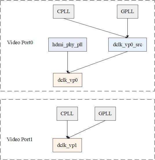
For the dclk on Video Port0, either hdmi_phy_pll or dclk_vp0_src can be specified as its parent clock. For dclk_vp0_src, either CPLL or GPLL can be specified as its parent clock.
For the dclk on Video Port1, either CPLL or GPLL can be specified as its parent clock.
The characteristics of hdmi_phy_pll are as follows:
Supports arbitrary frequency division
CPLL and GPLL have the following characteristics:
Share the PLL with other IP modules
Do not support arbitrary frequency division, and the output frequency is an integer multiple of the PLL frequency
By default, HDMI uses hdmi_phy_pll as the parent clock of dclk, which can meet various frequency requirements. CVBS has only a few fixed output resolutions, and only a few fixed dclk frequency points are required. Using CPLL or GPLL as the parent clock can meet the frequency requirements of these output resolutions.
4.5.3 RK3562 VOP DCLK Allocation Strategy
4.5.3.1 RK3562 DCLK Overview
RK3562 has only 1 Video Port. The dclk tree of the Video Port is shown in the following figure:
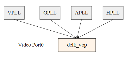
The dclk can specify one of VPLL, GPLL, and APLL as its parent clock. HPLL is currently allocated to audio for exclusive use and cannot be used by VOP.
VPLL has the following characteristics:
Can be allocated to VOP for exclusive use
Supports output of any frequency
VPLL is the default parent clock of VP0
GPLL and APLL have the following characteristics:
Share the PLL with other IP modules
Do not support arbitrary frequency division, and the output frequency is an integer multiple of the PLL frequency
By default, using VPLL as the parent clock of VP0 can meet various frequency requirements.
4.5.4 RK3568 VOP DCLK Allocation Strategy
4.5.4.1 RK3568 DCLK Overview
RK3568 has 3 Video Ports. The dclk tree of each Video Port is shown in the following figure:
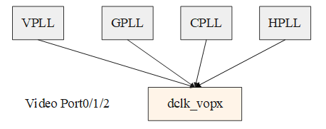
For the dclk on all Video Ports, any one of VPLL, GPLL, CPLL, and HPLL can be specified as its parent clock.
VPLL and HPLL have the following characteristics:
Can be allocated to VOP for exclusive use
Support output of any frequency
HPLL is allocated to VP0 by default in the DTS, and VPLL is allocated to VP1 by default in the DTS:
assigned-clocks = <&cru DCLK_VOP0>, <&cru DCLK_VOP1>, <&cru DCLK_VOP2>;
assigned-clock-parents = <&pmucru PLL_HPLL>, <&cru PLL_VPLL>, <&cru PLL_GPLL>;
GPLL and CPLL have the following characteristics:
Share the PLL with other IP modules
Do not support arbitrary frequency division, and the output frequency is an integer multiple of the PLL frequency
4.5.5 RK3576 VOP DCLK Allocation Strategy
4.5.5.1 RK3576 DCLK Overview
RK3576 has 3 Video Ports. The dclk tree of each Video Port is shown in the following figure:
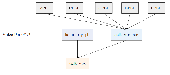
For the dclk on all Video Ports, either hdmi_phy_pll or dclk_vpx_src0/1/2 can be specified as its parent clock. For dclk_vpx_src0/1/2, one of VPLL, CPLL, GPLL, BPLL, and LPLL can be specified as its parent clock.
Among them, VPLL, CPLL, GPLL, BPLL, and LPLL are the PLLs on the system CRU, and hdmi_phy_pll is the PLL on the HDMI PHY.
VPLL has the following characteristics:
This PLL can be allocated to VOP for exclusive use.
Supports output of any frequency.
It is allocated to VP2 by default in the DTS:
&vp2 {
  assigned-clocks = <&cru DCLK_VP2_SRC>;
  assigned-clock-parents = <&cru PLL_VPLL>;
};
CPLL, GPLL, BPLL, and LPLL have the following characteristics:
Share the PLL with other IP modules
Do not support arbitrary frequency division, and the output frequency is an integer multiple of the PLL frequency
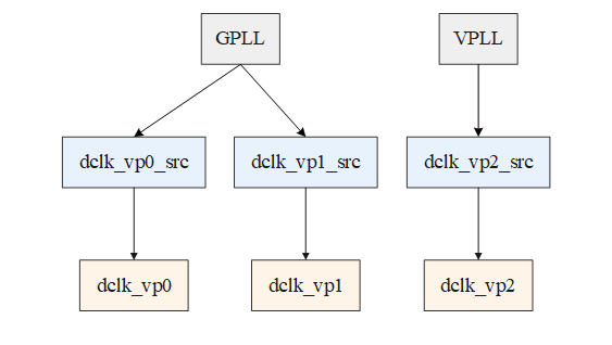
dclk_vp0/1/ is bound to GPLL by default
Among them, BPLL and LPLL are less used. BPLL is used by the CPU by default. If VOP needs to use it, the CPU’s PLL needs to be switched to PVTPLL. In addition, the frequency division of BPLL can only be a multiple of 2, 3, 4, 6, or 8.
The binding relationships of the default parent clocks of each Video Port are as follows:
The characteristics of hdmi_phy_pll are as follows:
-
Supports arbitrary frequency division
-
When HDMI is not working, VOP exclusively use the PLL. When HDMI is working, it shares the PLL with the HDMI PHY.
-
HDMI and EDP share the PHY. When EDP is working, the PLL on the PHY cannot be used by VOP.
The second and third characteristics of hdmi_phy_pll lead to some limitations in use. For example:
1. When HDMI is working and Video Port0 is bound to HDMI, the scenarios in which each Video Port can use hdmi_phy_pll (similar when bound to Video Port1/2)
| HDMI PHY PLL | VP0_DCLK | VP1_DCLK | VP2_DCLK |
|---|---|---|---|
| hdmi_phy_pll | DCLK <= 600MHz, available; DCLK > 600MHz, unavailable | unavailable | unavailable |
2. When EDP is working and Video Port0 is bound to EDP, the scenarios in which each Video Port can use hdmi_phy_pll (similar when bound to Video Port1/2)
| HDMI PHY PLL | VP0_DCLK | VP1_DCLK | VP2_DCLK |
|---|---|---|---|
| hdmi_phy_pll | unavailable | unavailable | unavailable |
Since CPLL, GPLL, BPLL, and LPLL cannot achieve arbitrary frequency division when used as the Video Port dclk source. When accurate frequency division is required and the usage restrictions are met, the hdmi_phy_pll can be used as the parent clock of the Video Port dclk. Currently, there are three usage strategies for the hdmi_phy_pll:
-
Static allocation strategy. That is, hdmi_phy_pll is bound to the Video Port, and the Video Port fixedly uses hdmi_phy_pll as the dclk source.
-
Dynamic allocation strategy bound to the HDMI interface. That is, hdmi_phy_pll is bound to the HDMI interface. hdmi_phy_pll can only be allocated to the Video Port that uses the HDMI interface, and this Video Port can dynamically select whether to use CRU PLL or hdmi_phy_pll as the dclk source.
-
Dynamic allocation strategy. hdmi_phy_pll is opened to all available VPs and interfaces. This dynamic allocation strategy is the most complex, and the application needs to consider whether the enabling of interfaces and Video Ports will lead to conflicts in the use of hdmi_phy_pll. Currently, it is only provided for NVR products.
For the allocation scheme of the dclk source used in general products, the first two can meet the requirements.
4.5.5.2 RK3576 VOP DCLK Static Allocation Strategy
The static allocation strategy has the following limitations:
1. In normal case, one hdmi_phy_pll can only be assigned to one Video Port (including VP0, VP1, VP2).
2. When the HDMI interface is working, the corresponding hdmi_phy_pll can only be assigned to the Video Port corresponding
to this HDMI interface, or not be used as the dclk source.
3. When the HDMI interface is working and the corresponding hdmi_phy_pll is assigned to the Video Port corresponding to this HDMI interface, the pixel clock of the output resolution can not exceed 600MHz.
4. When the EDP interface (sharing the phy with the HDMI interface) is working, the corresponding hdmi_phy_pll cannot be used as the dclk source for the Video Port.
Static allocation means binding the Video Port dclk parent in the dtsi. After the binding relationship is configured in the dtsi, it will not change.
&hdptxphy_hdmi {
  status = "okay";
};

&vp0 {
  assigned-clocks = <&cru DCLK_VP0>;
  assigned-clock-parents = <&hdptxphy_hdmi>;
};
As above, the parent clock of dclk_vp0 is bound to hdmi_phy_pll.
The effectiveness of the configuration can be confirmed through the clock tree, as follows:
rk3588_s:/ # cat /sys/kernel/debug/clk/clk_summary | grep "hdmiphy" -A 4
    clk_hdmiphy_pixel0 1   2    0     132000000 0   0  50000  ?
 27da0000.hdmi      link_clk

 display-subsystem  hdmi0_phy_pll

 hdmi@27da0000      no_connection_id
 deviceless         no_connection_id
      dclk_vp0        1    3    0     132000000 0   0  50000  Y
   27d00000.vop       dclk_vp0
As above, the parent clock binding takes effect, and the current clock rate set for dclk_vp0 is 132MHz. The clock rate here is the same as the clock rate obtained from the log print.
In the following log, the last line set dclk_vp0 to 132000000, get 132000000 means setting 132MHz, and the actual output is also 132MHz, which is the same as that obtained from the clk tree.
[  5.598827][ T331] rockchip-vop2 27d00000.vop: [drm:vop2_crtc_atomic_enable] Update mode to 1080x1920p60, type: 16(if:MIPI0, flag:0x0) for vp0 dclk: 132000000
[  5.599012][ T331] rockchip-hdptx-phy-hdmi 2b000000.hdmiphy: hdptx_ropll_cmn_config bus_width:0 rate:742500
[  5.599185][ T331] rockchip-hdptx-phy-hdmi 2b000000.hdmiphy: hdptx phy pll locked!
[  5.599237][ T331] rockchip-hdptx-phy-hdmi 2b000000.hdmiphy: hdptx_ropll_cmn_config bus_width:0 rate:1320000
[  5.599415][ T331] rockchip-hdptx-phy-hdmi 2b000000.hdmiphy: hdptx phy pll locked!
[  5.599423][ T331] rockchip-vop2 27d00000.vop: [drm:vop2_crtc_atomic_enable] set dclk_vp0 to 132000000, get 132000000
4.5.5.3 RK3576 VOP DCLK Dynamic Allocation Strategy Bound to HDMI Interface
The hdmi_phy_pll can only be allocated to the Video Port that uses the HDMI interface. This Video Port can dynamically switch the dclk source between the CRU PLL and the hdmi_phy_pll according to the working mode of the HDMI interface. The corresponding configuration is as follows:
&hdptxphy_hdmi {
  status = "okay";
};

&display_subsystem {
  clocks = <&hdptxphy_hdmi>;
  clock-names = "hdmi0_phy_pll";
};
For the above mentioned configuration, if HDMI0 is bound to VP0, the corresponding dclk source will be switched according to the pixel clock of the resolution, as shown in the following table:
| pixel clock > 600MHz | pixel clock < 600MHz | |
|---|---|---|
| VP0–>HDMI0 | CRU PLL | hdmi0 phy pll |
4.5.5.4 RK3576 VOP DCLK Dynamic Allocation Strategy
To use the dynamic binding strategy, the following configuration is required in the dtsi:
&hdptxphy_hdmi {
  status = "okay";
};

&display_subsystem {
  clocks = <&hdptxphy_hdmi>;
  clock-names = "hdmi0_phy_pll";
};
&vop {
  rockchip,extend-phy-pll-shared-mode;
};
It can be seen from the dts configuration that compared with the second strategy, the dynamic allocation test only has an additional rockchip,extend-phy-pll-shared-mode property configured under the vop node.
Since the PLL sources that can perform arbitrary frequency division are limited, and the use of the PLL on the HDMI PHY has certain restrictions, the dynamic allocation strategy is relatively complex. At the same time, the dynamic allocation strategy has certain restrictions on the business scenarios.
Each time a Video Port is enabled, the dynamic binding of the Video Port dclk will be carried out according to the following strategy:
1. HDMI (possibly including DP or MIPI hanging under the same Video Port) is connected to one Video Port(0/1/2), hereinafter referred to as VP_A, and the dclk is below 600MHz:
When hdmi_phy_pll is configured and not used by other Video Ports, VP_A uses hdmi_phy0_pll;
When hdmi_phy_pll is configured and used by other Video Ports, an error is reported;
2. When only DP is connected to one Video Port(0/1/2):
When the Video Port is Video Port2, use the default configured dclk parent clock, that is, VPLL;
When hdmi_phy_pll is not used by other Video Ports, give priority to using hdmi_phy_pll, otherwise use the default configured dclk parent clock;
If the required dclk is greater than 4k@60Hz, use the default pll.
According to the dynamic configuration strategy, in order to make the most of hdmi_phy0_pll, the following suggestions are given for actual use:
The VP corresponding to HDMI should try not to set the parent clock as VPLL.
For some application scenarios of RK3576, the following configuration suggestions for Video Ports and display interfaces are given:
When there is 1 HDMI interface and 1 DP interface output:
| Video Port | Interface Configuration 1 | Interface Configuration 2 |
|---|---|---|
| Video Port0 | HDMI | Other display interface |
| Video Port1 | Other display interface | HDMI |
| Video Port2 | DP | DP |
In this configuration, DP uses VPLL on VP2, and HDMI uses hdmi_phy_pll on VP0, so both interfaces can obtain accurate frequencies.
If the parent clock of DP is not VPLL, it will try to obtain hdmi_phy_pll. If hdmi_phy_pll has been occupied by HDMI at this time, the following prompt will appear:
[ 71.673928][ T397] rockchip-vop2 27d00000.vop: [drm:vop2_crtc_atomic_enable] Update mode to 2560x1440p60, type: 1lag:0x0) for vp1 dclk: 241500000
[ 71.674040][ T397] [drm] No free hdmi phy pll for DP, use default parent
[ 71.674088][ T397] rockchip-vop2 27d00000.vop: [drm:vop2_crtc_atomic_enable] set dclk_vp1 to 241500000, get 23760
In this case, DP will use the current default clock parent and may not be able to obtain an accurate clock frequency.
4.5.5.5 Selection of RK3576 VOP DCLK Allocation Strategies
The above three strategies are mainly designed to meet the requirements of arbitrary frequency division for HDMI and DP interfaces. In most application scenarios, the dynamic allocation strategy of the HDMI interface can meet the requirements. The following lists the DCLK allocation strategies for some scenarios.
(1) Three Port outputs, with DP and HDMI required to meet arbitrary frequency division
| Video Port | Interface |
|---|---|
| VP0 | HDMI |
| VP1 | DP |
| VP2 | DSI |
Use the dynamic switching strategy bound to the HDMI interface. When the pixel clock of the HDMI interface does not exceed 600MHz, the dclk source of the corresponding VP0 selects the hdmi phy pll to meet arbitrary frequency division. When the pixel clock is greater than or equal to 600MHz, use the CRU PLL for integer division and filter out some unsupported resolutions. The dclk source of VP1 corresponding to the DP interface uses VPLL to meet the requirement of arbitrary frequency division.
The DTS configuration is as follows:
&hdptxphy_hdmi {
  status = "okay";
};

&display_subsystem {
  clocks = <&hdptxphy_hdmi>;
  clock-names = "hdmi0_phy_pll";
};
&vp1 {
  assigned-clocks = <&cru DCLK_VP1_SRC>;
  assigned-clock-parents = <&cru PLL_VPLL>;
};
(2) Dual 4K configuration scenario, with the DP interface as the main screen. This scenario supports VP0 output to DP + HDMI, or VP0 output to DP and VP1 output to HDMI. And the pixel clocks of both VP0 and VP1 outputs are below 600MHz. These two scenarios can be switched, and both need to support arbitrary frequency division, that is:
| Video Port | Interface |
|---|---|
| VP0 | DP + HDMI |
or
| Video Port | Interface |
|---|---|
| VP0 | DP |
| VP1 | HDMI |
In this scenario, since the HDMI interface may switch VP, use the static allocation strategy. The dclk source of VP0 is fixed to use VPLL, and the dclk source of VP1 is fixed to use the hdm phy pll. The DTS configuration is as follows:
&hdptxphy_hdmi {
  status = "okay";
};

&vp0 {
  assigned-clocks = <&cru DCLK_VP0_SRC>;
  assigned-clock-parents = <&cru PLL_VPLL>;
};
&vp1 {
  assigned-clocks = <&cru DCLK_VP1>;
  assigned-clock-parents = <&hdptxphy_hdmi>;
};
(3) Scenarios where interfaces can switch VP arbitrarily and meet the arbitrary frequency division requirements of different interfaces. That is, different interfaces may switch between different VPs for use. This is a relatively complex usage scenario (currently only used in the NVR scenario). For example, HDMI/DP/DSI can all switch to use VP0/1/2 in this scenario:
| Video Port | Interface |
|---|---|
| VP0, VP1, VP2 | HDMI |
| VP0, VP1, VP2 | DP |
| VP0, VP1, VP2 | DSI |
Use the following dynamic allocation strategy in this scenario. The DTS configuration is as follows:
&hdptxphy_hdmi {
  status = "okay";
};

&display_subsystem {
  clocks = <&hdptxphy_hdmi>;
  clock-names = "hdmi0_phy_pll";
};
&vop {
  rockchip,extend-phy-pll-shared-mode;
};

&vp2 {
  assigned-clocks = <&cru DCLK_VP2_SRC>;
  assigned-clock-parents = <&cru PLL_VPLL>;
};
In the above configuration, assume that initially, only DP uses VP2 and HDMI uses VP0. The dclk source binding relationship is as follows:
| route | dclk source |
|---|---|
| VP0->HDMI | hdmi phy pll |
| VP2->DP | VPLL |
After that, if the HDMI is unplugged, the DP is connected to VP1, and the DSI is connected to VP2, then the DP uses the hdmi phy pll, and the DSI uses VPLL:
| route | dclk source |
|---|---|
| VP1->DP | hdmi phy pll |
| VP2->DSI | VPLL |
In the dynamic allocation strategy of this scenario, when the HDMI interface uses VP, it selects the corresponding hdmi phy pll, and it is necessary to ensure that the hdmi phy pll is not used by other interfaces. When non-HDMI interfaces use VP, if the corresponding VP source is not VPLL and the hdmi phy pll is not occupied by other interfaces, the hdmi phy pll can be used as the dclk source. When using the dynamic allocation strategy, the application needs to ensure that the corresponding hdmi phy pll is not occupied by other interfaces before enabling the HDMI interface.
4.5.6 RK3588 VOP DCLK Allocation Strategy
4.5.6.1 RK3588 DCLK Overview
RK3588 has 4 Video Ports. The dclk tree of each Video Port is shown in the following figure:
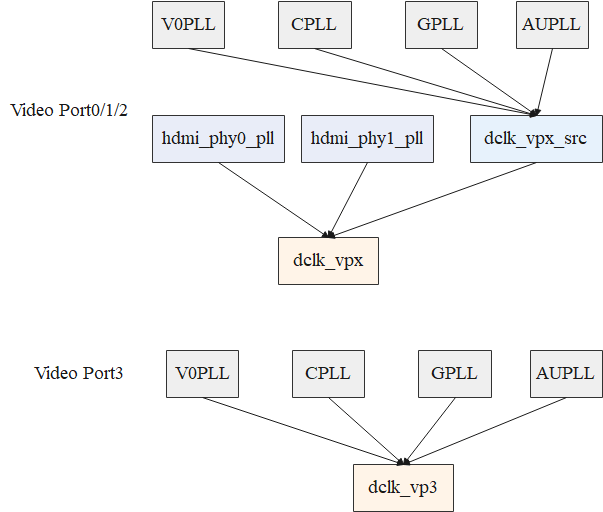
For dclk_vp0/1/2, one of hdmi_phy0_pll, hdmi_phy1_pll, dclk_vpx_src0/1/2 can be specified as its parent clock. For dclk_vpx_src0/1/2, V0PLL, CPLL, GPLL, AUPLL can be specified as its parent clock.
For dclk_vp3, V0PLL, CPLL, GPLL, AUPLL can be specified as its parent clock.
V0PLL, CPLL, GPLL, AUPLL are the PLLs on the system CRU, and hdmi_phy0_pll and hdmi_phy1_pll are the PLLs on the HDMI PHY.
The characteristics of V0PLL are as follows:
-
This PLL is generally allocated to VOP for exclusive use.
-
Supports any frequency.
-
It is bound to dclk_vp2 by default in the dts, and the code is as follows:
vp2: port@2 {
  assigned-clocks = <&cru DCLK_VOP2_SRC>;
  assigned-clock-parents = <&cru PLL_V0PLL>;
}
The characteristics of CPLL, GPLL, AUPLL are as follows:
-
Share the PLL with other IP modules.
-
Do not support arbitrary frequency division, and the output frequency is an integer multiple of the PLL frequency.
-
dclk_vp0/1/3 is bound to GPLL by default.
The binding relationships of the default parent clocks of each Video Port are as follows:
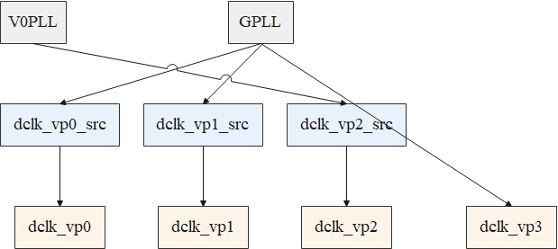
The characteristics of hdmi_phy0_pll and hdmi_phy1_pll are as follows:
-
Support arbitrary frequency division.
-
When HDMI is not working, VOP exclusively occupies the PLL. When HDMI is working, VOP shares the PLL with the HDMI PHY.
-
HDMI and EDP share the PHY. When EDP is working, the PLL on the PHY cannot be used by VOP.
The second and third characteristics of hdmi_phy0_pll and hdmi_phy1_pll lead to some limitations in use. For example:
1. When HDMI0 is working and Video Port0 is bound to HDMI0, the scenarios in which each Video Port can use hdmi_phy0_pll and hdmi_phy1_pll (similar when bound to Video Port1/2)
| HDMI PHY PLL | VP0_DCLK | VP1_DCLK | VP2_DCLK |
|---|---|---|---|
| hdmi_phy0_pll | DCLK <= 600MHz, available; DCLK > 600MHz, unavailable | unavailable | unavailable |
| hdmi_phy1_pll | available | available | available |
2. When HDMI1 is working and Video Port0 is bound to HDMI1, the scenarios in which each Video Port can use hdmi_phy0_pll and hdmi_phy1_pll (similar when bound to Video Port1/2)
| HDMI PHY PLL | VP0 DCLK | VP1_DCLK | VP2_DCLK |
|---|---|---|---|
| hdmi_phy0_pll | available | available | available |
| hdmi_phy1_pll | DCLK <= 600MHz, available DCLK > 600MHz, unavailable | unavailable | unavailable |
3. When HDMI0 and HDMI1 are working simultaneously and both are bound to Video Port0, the scenarios in which the Video Port can use hdmi_phy0_pll and hdmi_phy1_pll (similar when bound to Video Port1/2)
| HDMI PHY PLL | VP0_DCLK | VP1_DCLK | VP2_DCLK |
|---|---|---|---|
| hdmi_phy0_pll | DCLK <= 600MHz, available; DCLK > 600MHz, unavailable | unavailable | unavailable |
| hdmi_phy1_pll | DCLK <= 600MHz, available; DCLK > 600MHz, unavailable | unavailable | unavailable |
4. When EDP0 is working and Video Port0 is bound to EDP0, the scenarios in which each Video Port can use hdmi_phy0_pll and hdmi_phy1_pll (similar when bound to Video Port1/2)
| HDMI PHY PLL | VP0_DCLK | VP1_DCLK | VP2_DCLK |
|---|---|---|---|
| hdmi_phy0_pll | unavailable | unavailable | unavailable |
| hdmi_phy1_pll | available | available | available |
5. When EDP1 is working and Video Port0 is bound to EDP1, the scenarios in which each Video Port can use hdmi_phy0_pll and hdmi_phy1_pll (similar when bound to Video Port1/2)
| HDMI PHY PLL | VP0 DCLK | VP1_DCLK | VP2_DCLK |
|---|---|---|---|
| hdmi_phy0_pll | available | available | available |
| hdmi_phy1_pll | unavailable | unavailable | unavailable |
6. When EDP0 and EDP1 are working simultaneously and both are bound to Video Port0, the scenarios in which the Video Port can use hdmi_phy0_pll and hdmi_phy1_pll (similar when bound to Video Port1/2)
| HDMI PHY PLL | VP0_DCLK | VP1_DCLK | VP2_DCLK |
|---|---|---|---|
| hdmi_phy0_pll | unavailable | unavailable | unavailable |
| hdmi_phy1_pll | unavailable | unavailable | unavailable |
Since CPLL, GPLL, AUPLL cannot achieve arbitrary frequency division when used as the dclk source of the Video Port. When accurate frequency division is required and the usage restrictions are met, hdmi_phy0_pll or hdmi_phy1_pll can be used as the parent clock of the Video Port dclk. Currently, there are three usage strategies for hdmi_phy_pll:
-
Static allocation strategy. That is, hdmi_phy_pll is bound to the Video Port, and the Video Port fixedly uses hdmi_phy_pll as the dclk source.
-
Dynamic allocation strategy bound to the HDMI interface. That is, hdmi_phy_pll is bound to the HDMI interface. The hdmi_phy_pll can only be allocated to the Video Port that uses the HDMI interface, and this Video Port can dynamically select whether to use CRU PLL or hdmi_phy_pll as the dclk source.
-
Dynamic allocation strategy. The hdmi_phy_pll is opened to all available VPs and interfaces. This dynamic allocation strategy is the most complex, and the application needs to consider whether the enabling of interfaces and Video Ports will lead to conflicts in the use of hdmi_phy_pll. Currently, it is only provided for NVR products.
For the allocation scheme of the dclk source used in general products, the first two can meet the requirements.
4.5.6.2 RK3588 VOP DCLK Static Allocation Strategy
The static allocation strategy has the following limitations:
-
In normal case, one hdmi_phy_pll can only be assigned to one Video Port (including VP0, VP1, VP2).
-
When the HDMI interface is working, the corresponding hdmi_phy_pll can only be assigned to the Video Port corresponding to this HDMI interface, or not be used as the dclk source.
-
When the HDMI interface is working and the corresponding hdmi_phy_pll is assigned to the Video Port corresponding to this HDMI interface, the pixel clock of the output resolution can not exceed 600MHz.
-
When the EDP interface (sharing the phy with the HDMI interface) is working, the corresponding hdmi_phy_pll cannot be used as the dclk source for the Video Port.
Static allocation means binding the Video Port dclk parent in the dtsi. After the binding relationship is configured in the dtsi, it will not change.
The reference configuration for kernel 5.10 is as follows:
&hdptxphy_hdmi0 {
  status = "okay";
};

&hdptxphy_hdmi1 {
  status = "okay";
};
&hdptxphy_hdmi_clk0 {
  status = "okay";
};

&hdptxphy_hdmi_clk1 {
  status = "okay";
};

&vp0 {
  assigned-clocks = <&cru DCLK_VOP0>;
  assigned-clock-parents = <&hdptxphy_hdmi_clk0>;
};
&vp1 {
  assigned-clocks = <&cru DCLK_VOP1>;
  assigned-clock-parents = <&hdptxphy_hdmi_clk1>;
};
The reference configuration for kernel version 6.1 and above is as follows:
&hdptxphy_hdmi0 {
  status = "okay";
};

&hdptxphy_hdmi1 {
  status = "okay";
};
&vp0 {
  assigned-clocks = <&cru DCLK_VOP0>;
  assigned-clock-parents = <&hdptxphy_hdmi0>;
};

&vp1 {
  assigned-clocks = <&cru DCLK_VOP1>;
  assigned-clock-parents = <&hdptxphy_hdmi1>;
};
As above, the parent clock of dclk_vp0 is bound to hdmi_phy0_pll, and the parent clock of dclk_vp1 is bound to hdmi_phy1_pll.
The effectiveness of the configuration can be confirmed through the clock tree, as follows:
rk3588_s:/ # cat /sys/kernel/debug/clk/clk_summary | grep "hdmiphy" -A 1
    clk_hdmiphy_pixel1 0    1     0      0     0   0 50000
      dclk_vop1        0    3     0      0     0   0 50000
    clk_hdmiphy_pixel0 1    1     0 148500000  0   0 50000
      dclk_vop0        2    5     0 148500000  0   0 50000
As above, the parent clock binding takes effect, and the current clock rate set for dclk_vp0 is 148.5MHz. The clock rate here is the same as the clock rate obtained from the log print.
In the following log, the last line set dclk_vop0 to 148500000, get 148500000 means setting 148.5MHz, and the actual output is also 148.5MHz, which is the same as that obtained from the clk tree.
[ 270.974623][ T381] rockchip-vop2 fdd90000.vop: [drm:vop2_crtc_atomic_enable] Update mode to 1920x1080p60, type: 11(if:800) for vp0 dclk: 148500000
[ 270.974837][ T381] rockchip-vop2 fdd90000.vop: [drm:vop2_crtc_atomic_enable] dclk_out0 div: 0 dclk_core0 div: 2
[ 270.974891][ T381] rockchip-hdptx-phy-hdmi fed60000.hdmiphy: hdptx_ropll_cmn_config bus_width:16a8c8 rate:1485000
[ 270.975264][ T381] rockchip-hdptx-phy-hdmi fed60000.hdmiphy: hdptx phy pll locked!
[ 270.975304][ T381] rockchip-vop2 fdd90000.vop: [drm:vop2_crtc_atomic_enable] set dclk_vop0 to 148500000, get 148500000
4.5.6.3 Dynamic Allocation Strategy for Binding RK3588 VOP DCLK and HDMI Interface
The hdmi_phy_pll can only be allocated to the Video Port that uses the HDMI interface. This Video Port can dynamically switch the dclk source between the CRU PLL and the hdmi phy pll according to the working mode of the HDMI interface. The corresponding kernel 5.10 configuration is as follows:
&hdptxphy_hdmi0 {
  status = "okay";
};

&hdptxphy_hdmi1 {
  status = "okay";
};
&hdptxphy_hdmi_clk0 {
  status = "okay";
};

&hdptxphy_hdmi_clk1 {
  status = "okay";
};

&display_subsystem {
  clocks = <&hdptxphy_hdmi_clk0>, <&hdptxphy_hdmi_clk1>;
  clock-names = "hdmi0_phy_pll", "hdmi1_phy_pll";
};
The reference configuration for kernel version 6.1 and above is as follows:
&hdptxphy_hdmi0 {
  status = "okay";
};

&hdptxphy_hdmi1 {
  status = "okay";
};
&display_subsystem {
  clocks = <&hdptxphy_hdmi0>, <&hdptxphy_hdmi1>;
  clock-names = "hdmi0_phy_pll", "hdmi1_phy_pll";
};
For the above configuration, if HDMI0 is bound to VP0 and HDMI1 is bound to VP1, the corresponding dclk source will switch according to the pixel clock of the resolution, as shown in the following table:
| pixel clock > 600MHz | pixel clock < 600MHz | |
|---|---|---|
| VP0–>HDMI0 | CRU PLL | hdmi0 phy pll |
| VP1–>HDMI1 | CRU PLL | hdmi1 phy pll |
4.5.6.4 RK3588 VOP DCLK Dynamic Allocation Strategy
The corresponding kernel 5.10 configuration for dynamic allocation is as follows:
&hdptxphy_hdmi0 {
  status = "okay";
};

&hdptxphy_hdmi1 {
  status = "okay";
};
&hdptxphy_hdmi_clk0 {
  status = "okay";
};

&hdptxphy_hdmi_clk1 {
  status = "okay";
};

&display_subsystem {
  clocks = <&hdptxphy_hdmi_clk0>, <&hdptxphy_hdmi_clk1>;
  clock-names = "hdmi0_phy_pll", "hdmi1_phy_pll";
};
&vop {
  rockchip,extend-phy-pll-shared-mode;
};
The reference configuration for kernel version 6.1 and above is as follows:
&hdptxphy_hdmi0 {
  status = "okay";
};

&hdptxphy_hdmi1 {
  status = "okay";
};
&display_subsystem {
  clocks = <&hdptxphy_hdmi0>, <&hdptxphy_hdmi1>;
  clock-names = "hdmi0_phy_pll", "hdmi1_phy_pll";
};

&vop {
  rockchip,extend-phy-pll-shared-mode;
};
It can be seen from the dts configuration that compared with the second strategy, the dynamic allocation test only has an additional rockchip,extend-phy-pll-shared-mode property configured under the vop node.
Since the PLL sources that can perform arbitrary frequency division are limited, and the use of the PLL on the HDMI PHY has certain restrictions, the dynamic allocation strategy is relatively complex. At the same time, the dynamic allocation strategy has certain restrictions on the business scenarios.
Each time a Video Port is enabled, the dynamic binding of the Video Port dclk will be carried out according to the following strategy:
1. HDMI0 and HDMI1 (possibly including DP or MIPI hanging under the same Video Port) are connected to the same Video Port(0/1/2) and the dclk is below 600MHz:
1.1 When both hdmi_phy0_pll and hdmi_phy1_pll are not used by other Video Ports, use hdmi_phy0_pll as the parent clock of the current Video Port dclk, and hdmi_phy0_pll and hdmi_phy1_pll cannot be used by other Video Ports;
1.2 When either hdmi_phy0_pll or hdmi_phy1_pll is used by other Video Ports, an error is reported;
2. HDMI0 (possibly including DP or MIPI hanging under the same Video Port) is connected to one Video Port(0/1/2), hereinafter referred to as VP_A, and the dclk is below 600MHz:
2.1 When both hdmi_phy0_pll and hdmi_phy1_pll exist and hdmi_phy0_pll is not used by other Video Ports, VP_A uses hdmi_phy0_pll, and hdmi_phy0_pll cannot be used by other Video Ports;
2.2 When both hdmi_phy0_pll and hdmi_phy1_pll exist and hdmi_phy0_pll is being used by another Video Port(VP_B), and hdmi_phy1_pll is idle, VP_B should give up hdmi_phy0_pll and use hdmi_phy1_pll, and VP_A uses hdmi_phy0_pll;
2.3 When both hdmi_phy0_pll and hdmi_phy1_pll exist and are used by other Video Ports, an error is reported;
2.4 When only hdmi_phy0_pll is configured and not used by other Video Ports, VP_A uses hdmi_phy0_pll;
2.5 When only hdmi_phy0_pll is configured and used by other Video Ports, an error is reported;
3. HDMI1 (possibly including DP or MIPI hanging under the same Video Port) is connected to one Video Port(0/1/2) and the dclk is below 600MHz, the strategy is similar to 2 and will not be described in detail;
4. When only DP is connected to one Video Port(0/1/2):
4.1 When the Video Port is Video Port2, use the default configured dclk parent clock;
4.2 When either hdmi_phy0_pll or hdmi_phy1_pll is not used by other Video Ports, give priority to using hdmi_phy0_pll or hdmi phy1_pll, otherwise use the default configured dclk parent clock;
If the required dclk is greater than 4k@60Hz, use the default pll.
According to the dynamic configuration strategy, in order to make the most of hdmi_phy0_pll and hdmi_phy1_pll, the following suggestions are given for actual use:
-
HDMI0 and HDMI1 should try not to be hung on Video Port2.
-
HDMI0 and HDMI1 should try not to be hung on the same Video Port.
For some application scenarios, the following configuration suggestions for Video Ports and display interfaces are given:
When there are 2 HDMI interfaces and 1 DP interface output:
| Video Port | Interface Configuration 1 | Interface Configuration 2 |
|---|---|---|
| Video Port0 | HDMI0 | HDMI1 |
| Video Port1 | HDMI1 | HDMI0 |
| Video Port2 | DP0/DP1 | DP0/DP1 |
When there are 2 DP interfaces and 1 HDMI interface output:
| Video Port |
Interface Configuration 1 |
Interface Configuration 2 |
Interface Configuration 3 |
Interface Configuration 4 |
|---|---|---|---|---|
| Video Port0 |
HDMI0/1 | HDMI0/1 | DP0 | DP1 |
| Video Port1 |
DP0 | DP1 | HDMI0/1 | HDMI0/1 |
| Video Port2 |
DP1 | DP0 | DP1 | DP0 |
For more application scenarios, reasonable configurations need to be made by referring to the dynamic allocation strategy.
The dynamic allocation strategy may result in the situation where both HDMI PHY PLLs are occupied. At this time, the occupation information of the HDMI PHY PLL will be printed in the log:
[ 220.692900][ T383] rockchip-vop2 fdd90000.vop: [drm:vop2_crtc_atomic_enable] Update mode to 1920x1080p60, type: 11(if:1000) for vp1 dclk: 148500000
[ 220.693048][ T383] rockchip-vop2 fdd90000.vop: [drm:vop2_crtc_atomic_enable] dclk_out1 div: 0 dclk_core1 div: 2
[ 220.693094][ T383] [drm:vop2_clk_set_parent_extend.isra.61] *ERROR* hdmi1 phy pll is used by vp0:vp2
As above, it means that hdmi_phy0_pll has been occupied by Video Port0, and hdmi_phy1_pll has been occupied by Video Port2.
When only one HDMI PHY PLL is configured, for example:
&display_subsystem {
     clocks = <&hdptxphy_hdmi_clk0>;
     clock-names = "hdmi0_phy_pll";
};
When the following log appears, it indicates that hdmi_phy0_pll has been occupied by Video Port2.
[ 35.059306][ T386] rockchip-vop2 fdd90000.vop: [drm:vop2_crtc_atomic_enable] Update mode to 1920x1080p60, type: 11(if:800) for vp0 dclk: 148500000
[ 35.059416][ T386] rockchip-vop2 fdd90000.vop: [drm:vop2_crtc_atomic_enable] dclk_out0 div: 0 dclk_core0 div: 2
[ 35.059447][ T386] [drm:vop2_clk_set_parent_extend.isra.61] *ERROR* hdmi0: phy pll is used by vp2
4.5.6.5 Selection of RK3588 VOP DCLK Allocation Strategy
The above three strategies are mainly designed to meet the requirement that the HDMI and DP interfaces can be divided at any frequency. The dynamic allocation strategy of the HDMI interface can meet the requirements in most application scenarios. The following lists the DCLK allocation strategies for some scenarios.
(1) Four Video Ports are output, and both DP and HDMI are required to support any frequency division.
| Video Port | Interface |
|---|---|
| VP0 | HDMI0 |
| VP1 | HDMI1 |
| VP2 | DP0 |
| VP3 | DSI0 |
Use the dynamic switching strategy of the HDMI interface. When the pixel clock of the HDMI interface is less than or equal to 600MHz, select the hdmi phy pll as the dclk source, which can support any frequency division. When the pixel clock is greater than or equal to 600MHz, use the CRU PLL for integer frequency division to filter out some unsupported resolutions. For the VP2 corresponding to the DP0 interface, use VPLL to meet the requirement of any frequency division.
The DTS configuration for kernel version 6.1 and above is as follows:
&hdptxphy_hdmi0 {
  status = "okay";
};

&hdptxphy_hdmi1 {
  status = "okay";
};
&display_subsystem {
  clocks = <&hdptxphy_hdmi0>, <&hdptxphy_hdmi1>;
  clock-names = "hdmi0_phy_pll", "hdmi1_phy_pll";
};
&vp2 {
  assigned-clocks = <&cru DCLK_VP2_SRC>;
  assigned-clock-parents = <&cru PLL_V0PLL>;
};
(2) Four Video Ports are output, and both DP and HDMI are required to support any frequency division.
| Video Port | Interface |
|---|---|
| VP0 | HDMI0 |
| VP1 | DP0 |
| VP2 | DP1 |
| VP3 | DSI0 |
Use the dynamic switching strategy of the HDMI interface. When the pixel clock of the HDMI0 interface does not exceed 600MHz, select the hdmi phy pll as the dclk source for VP0, which can support any frequency division. When the pixel clock is greater than or equal to 600MHz, use the CRU PLL for integer frequency division to filter out some unsupported resolutions. For the DP0 interface, use the hdmi phy1 pll as the dclk source for VP1, and for the DP1 interface, use V0PLL as the dclk source for VP2, which can meet the requirement of any frequency division.
The DTS configuration for kernel version 6.1 and above is as follows:
&hdptxphy_hdmi0 {
  status = "okay";
};

&hdptxphy_hdmi1 {
  status = "okay";
};
&display_subsystem {
  clocks = <&hdptxphy_hdmi0>;
  clock-names = "hdmi0_phy_pll";
};

&vp1 {
  assigned-clocks = <&cru DCLK_VP1>;
  assigned-clock-parents = <&hdptxphy_hdmi1>;
};
&vp2 {
  assigned-clocks = <&cru DCLK_VP2_SRC>;
  assigned-clock-parents = <&cru PLL_V0PLL>;
};
(3) Scenarios where interfaces can switch VPs arbitrarily and meet the requirement of any frequency division for different interfaces. That is, different interfaces may switch and use different VPs. This is a relatively complex scenario (currently only used in the NVR scenario). For example, HDMI/DP/DSI can all switch and use VP0/1/2 in this scenario:
| Video Port | Interface |
|---|---|
| VP0, VP1, VP2 | HDMI0 |
| VP0, VP1, VP2 | HDMI1 |
| VP0, VP1, VP2 | DP0 |
| VP0, VP1, VP2 | DP1 |
For this scenario, use the following dynamic allocation strategy. The DTS configuration for kernel version 6.1 and above is as follows:
&hdptxphy_hdmi0 {
  status = "okay";
};

&hdptxphy_hdmi1 {
  status = "okay";
};
&display_subsystem {
  clocks = <&hdptxphy_hdmi0>, <&hdptxphy_hdmi1>;
  clock-names = "hdmi0_phy_pll", "hdmi1_phy_pll";
};

&vop {
  rockchip,extend-phy-pll-shared-mode;
};

&vp2 {
  assigned-clocks = <&cru DCLK_VP2_SRC>;
  assigned-clock-parents = <&cru PLL_V0PLL>;
};
For the above configuration, assume initially that HDMI0 uses VP0, HDMI1 uses VP1, and DP0 uses VP1, as follows:
| route | dclk source |
|---|---|
| VP0->HDMI0 | hdmi phy0 pll |
| VP1->HDMI1 | hdmi phy1 pll |
| VP2->DP0 | V0PLL |
After that, if both HDMI0 and HDMI1 are unplugged, HDMI1 is re - connected to VP0 first, and then DP1 is connected to VP1. The dclk source allocation is as follows:
| route | dclk source |
|---|---|
| VP0->HDMI1 | hdmi phy1 pll |
| VP1->DP1 | hdmi phy0 pll |
| VP2->DP0 | V0PLL |
In this scenario of the above dynamic allocation strategy, when the HDMI interface uses a VP, select the corresponding hdmi phy pll, and ensure that the hdmi phy pll is not used by other interfaces. When a non - HDMI interface uses a VP, if the corresponding VP source is not V0PLL and the hdmi phy pll is not occupied by other interfaces, the hdmi phy pll can be used as the dclk source. When using the dynamic allocation strategy, the application needs to ensure that the corresponding hdmi phy pll is not occupied by other interfaces before enabling the HDMI interface.
5. Multi-screen Display under VOP 2.0 Architecture
As introduced before, for chips adopting the VOP 1.0 architecture, if multi-screen different-display is to be achieved, multiple VOPs are generally required. Therefore, for VOP 1.0 architecture platforms, only chips with dual VOPs such as RK3288, RK3399, and PX30 support dual-screen different-display.
For chips with the VOP 2.0 architecture, due to the adoption of a unified display architecture, IP resources can be used more efficiently. Under the most basic conditions, the number of independent display outputs that can be achieved is equal to the number of Video Ports inside the VOP. According to the content of the VOP2 Platform Display Paths chapter, the RK3568 platform has three independent Video Ports, and the RK3588 platform has four independent Video Ports. Therefore, under the most basic conditions, RK3568 and RK3588 can achieve 3-way and 4-way independent display outputs respectively.
5.1 Connector-mirror
The Connector-mirror technology of VOP2 enables one Video Port to drive multiple display interfaces simultaneously, output the same display timing, and display the same content.
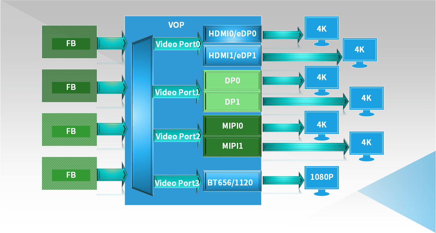
As shown in the figure, on RK3588, through the Connector-mirror technology, two HDMI/eDPs are connected to VP0, two DPs are connected to VP1, and two MIPI DSIs are connected to VP2. VP3 can output 7 channels simultaneously through BT656 and BT1120, with four groups of independent display outputs. The display timings of each group (two display interfaces on the same Video Port) are the same, and the displayed content is also the same.
In this application mode, the maximum resolution of each group of display paths is limited by the maximum resolution of the corresponding Video Port and display interface.
This display feature can be enabled through dts configuration. In the dts, just connect two display interfaces to the same VP:
&hdmi0 {
     status = "okay";
};

&hdmi1 {
     status = "okay";
};

&hdmi0_in_vp0 {
     status = "okay";
};
&hdmi1_in_vp0 {
     status = "okay";
};

&hdmi0_in_vp1 {
     status = "disabled";
};
&hdmi0_in_vp2 {
     status = "disabled";
};

&hdmi1_in_vp1 {
     status = "disabled";
};

&hdmi1_in_vp2 {
     status = "disabled";
};
This configuration connects HDMI0 and HDMI1 to VP0 and enables the connector-mirror function.
Currently, the NVR SDK supports this function, and Android needs to update to an hwc version later than 1.4.15 to support this feature.
5.2 Connector-split
The Connector-split function provided by VOP2 is a technology similar to the mipi dual-channel mode. It allows the output of one Video Port to be divided horizontally into two paths, simultaneously driving two display interfaces to display the same display timing but independent content.
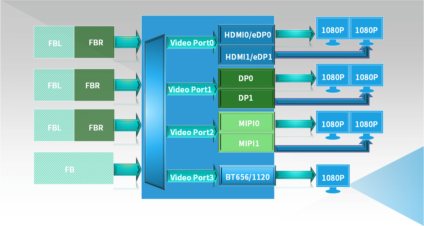
As shown in the above figure, if the split mode is enabled on VP0, the output of VP0 can simultaneously drive two display interfaces (HDMI0/1, eDP0/1, or other display interfaces that can be connected to VP0). The content displayed on the two display interfaces is the content of VP0’s output horizontally divided into left and right parts. For example, if VP0 outputs at a resolution of 3840x1080, each of the two display interfaces displays 1920x1080.
Through this technology, 7-way independent display outputs can be expanded on RK3588.
It should be noted that for the two display interfaces participating in the split output on each VP, the output timings and frame rates must be the same.
Through the Connector-split technology, more multi-screen different-display functions can be expanded. Currently, only RK3588/RK3576 support this function. Connector-split is divided into the following two modes according to the interface type:
1. Split mode for the same display interface: rockchip,split-mode
(1) One VP is connected to 2 interfaces/screens with exactly the same timing; (2) The two screens display the left-and right-half-screen images respectively; (3) The DTS configuration/EDID reads the timing of a single screen, and the driver passes the horizontal timing multiplied by 2 to the VOP by calling the interface: drm_mode_convert_to_split_mode() ; (4) The software registers 1 connector, and the application layer sees 1 display device;
In this mode, in the dts configuration file, the two display interfaces participating in the split are connected to the same VP, and the rockchip,split-mode attribute of the left-hand display interface is turned on.
For example, to turn on the split function of hdmi0 and hdmi1 on VP0 according to the following configuration:
&hdmi0 {
     status = "okay";
};

&hdmi1 {
     status = "okay";
     rockchip,split-mode;
};
&hdmi0_in_vp0 {
     status = "okay";
};

&hdmi1_in_vp0 {
     status = "okay";
};
&hdmi0_in_vp1 {
     status = "disabled";
};

&hdmi0_in_vp2 {
     status = "disabled";
};
&hdmi1_in_vp1 {
     status = "disabled";
};

&hdmi1_in_vp2 {
     status = "disabled";
};
In the driver implementation, in order to facilitate the adaptation of upper-layer applications and be as close as possible to the MIPI dual-channel technology, while shielding the underlying implementation differences, only one encoder and connector are registered to the drm system for the two display interfaces on each Video Port that perform split. Therefore, in user space, only one connector device is seen for each CRTC (Video Port). This information can be confirmed through the output of modetest.
For Android applications that expect each screen to correspond to an independent display device, the Android hwc on the Rockchip platform has been optimized accordingly. For specific details, please refer to the document 《DrmHwc2 Multi-screen Stitching and Different-display Function Description》.
2. Split mode for different display interfaces: rockchip,dual-connector-split
(1) One VP is connected to 2 interfaces with different interfaces but exactly the same timing; (2) The two screens display the left-and right-half-screen images respectively; (3) The DTS configuration/EDID reads the timing of a single screen, and the driver passes the horizontal timing multiplied by 2 to the VOP by calling the interface: drm_mode_convert_to_split_mode() ; (4) The software registers 2 connectors, and the application layer sees 2 display devices;
The main difference from rockchip,split-mode is the use of 2 different display interfaces. Since the DRM framework needs to manage the drivers of the 2 display interfaces separately, 2 connectors are registered, and the application layer sees 2 display devices. In this mode, the function can be turned on by configuring the attribute: rockchip,dual-connector-split under the corresponding interface node, and at the same time, the attribute: rockchip,left-display can be used to mark the left-hand screen.
For example, to turn on the split function of HDMI0 and DP0 on VP0 according to the following configuration, and HDMI0 displays the left-half-screen image:
&hdmi0 {
     status = "okay";
     rockchip,dual-connector-split;
     rockchip,left-display;
};

&dp0 {
     status = "okay";
     rockchip,dual-connector-split;
};
&hdmi0_in_vp0 {
     status = "okay";
};

&dp0_in_vp0 {
     status = "okay";
};
&hdmi0_in_vp1 {
     status = "disabled";
};

&hdmi0_in_vp2 {
     status = "disabled";
};

&dp0_in_vp1 {
     status = "disabled";
};
&dp0_in_vp2 {
     status = "disabled";
};
6. Hardware-related
6.1 Hardware Connection of RGB Output/TTL Mode
6.1.1 Hardware Connection Method of VOP 1.0 RGB Interface
1. To determine whether it is a VOP 1.0 or VOP 2.0 design, you can query from the VOP version in Chapter 3.1;
2. For the hardware connection method of SOC supporting 24-bit RGB output
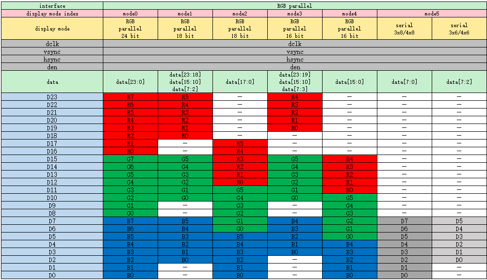
3. For the hardware connection method of SOC supporting 18-bit RGB output
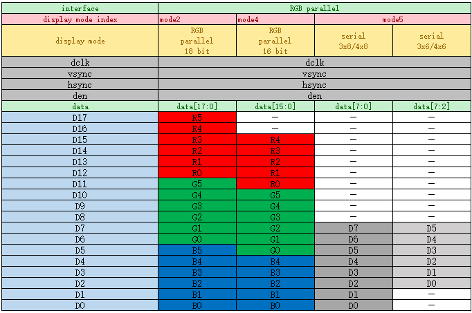
4. For the MCU interface in VOP 1.0, the connection method of the DATA line is the same as that of the RGB parallel connection. It should be noted that the 4 clock signals in the RGB parallel connection are multiplexed into the control signals of the MCU interface. The following is the specific correspondence:

6.1.2 Hardware Connection Method of RGB Interface in VOP 2.0 and Later Versions
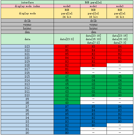
6.1.3 Software Configuration Corresponding to Different display mode index
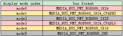
6.1.4 Hardware Connection Method of BT.656 and BT.1120

According to the different processing orders of Y/U/V at the receiving end, if the display color is incorrect, different bus_formats can be adjusted in the DTS for adaptation. BT.656 and BT.1120 have the following four configurations respectively:
BT.656:
#define MEDIA_BUS_FMT_UYVY8_2X8 0x2006
#define MEDIA_BUS_FMT_VYUY8_2X8 0x2007
#define MEDIA_BUS_FMT_YUYV8_2X8 0x2008
#define MEDIA_BUS_FMT_YVYU8_2X8 0x2009
BT.1120:
#define MEDIA_BUS_FMT_UYVY8_1X16 0x200f
#define MEDIA_BUS_FMT_VYUY8_1X16 0x2010
#define MEDIA_BUS_FMT_YUYV8_1X16 0x2011
#define MEDIA_BUS_FMT_YVYU8_1X16 0x2012
The definition of MEDIA_BUS_FMT can be referred to:
./include/uapi/linux/media-bus-format.h
6.2 LVDS Data Mapping
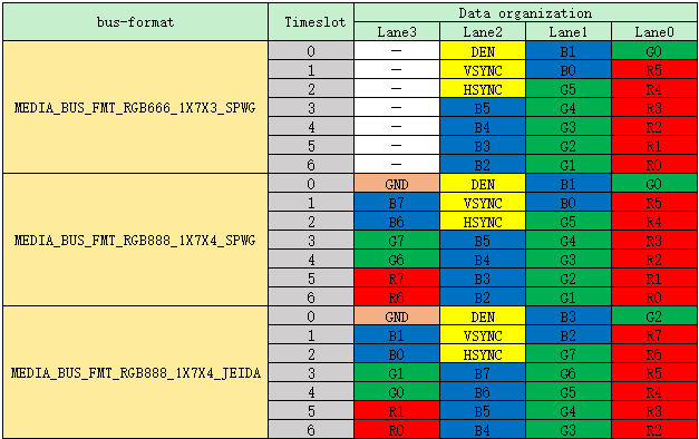
7. Scan Timing Instructions
7.1 Common Scan Timing Diagram
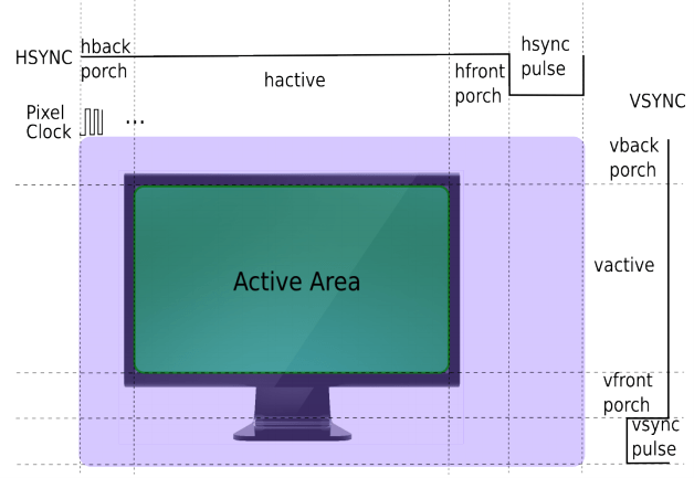
7.2 DRM’s Definition of Scan Timing
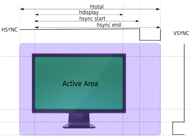
7.3 Corresponding Relationship and Conversion of Software Configuration
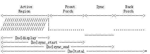
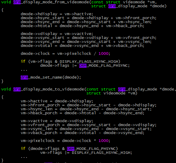
7.4 Viewing the Currently Configured Timing
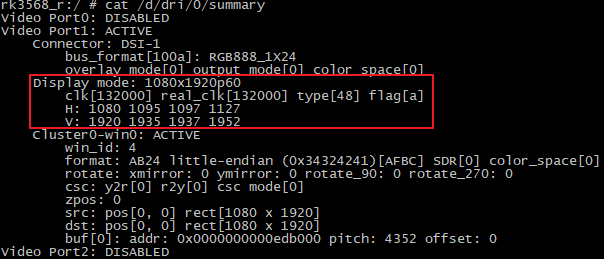
8. Bandwidth Calculation Method
8.1 Bandwidth of the Image
Taking 1080P ARGB-format image data as an example:
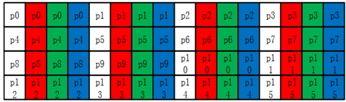
The memory size occupied by one pixel in ARGB format: 4 Byte
The memory occupied by 1080P ARGB-format data: 1920 x 1080 x 4Byte/pixel = 8,100 Kbyte
If refreshed at 60fps, the occupied bandwidth is: 8,100 x 60fps = 474.6 Mbyte/s
If the data format is changed to YUV420SP(NV12):
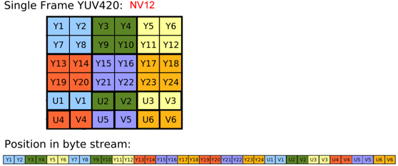
The memory size occupied by one pixel in NV12 format: 1.5 Byte
The memory occupied by 1080P NV12-format data: 1920 x 1080 x 1.5Byte/pixel = 3,037.5 Kbyte
If refreshed at 60fps, the occupied bandwidth is: 3,037.5 x 60fps = 178 Mbyte/s
8.2 Bandwidth of the Display Interface
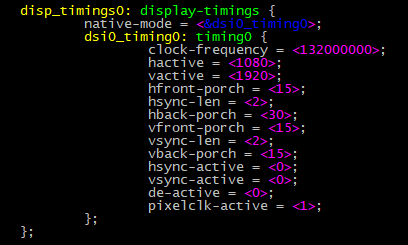
Taking the timing configured in the above figure as an example, the dclk required for 60-frame refresh under the current timing is: 131994240 hz, and the dts is actually configured as 132000000 hz after rounding:
htotal = hfp + hsync + hbp + hactive = 15 + 2 + 30 + 1080 = 1,127
vtotal = vfp + vsync + vbp + vactive = 15 + 2 + 15 + 1920 = 1,952
dclk = htotal x vtotal x fps = 1127 x 1952 x 60fps = 131,994,240
The frequency transmitted on the MIPI interface is:
132M x 3(RGB) x 8(bpc) / 4(lane) / 0.9 = 880 Mbps
Among them:
x3(RGB) : means each pixel has 3 components of RGB;
x8(bpc) : means the bit-depth of each component is 8bit;
/4(lane) : is to calculate the data volume per lane as the total data volume is transmitted on 4 lanes;
/0.9 : is to consider the transmission efficiency of the mipi timing.
9. Common Debugging Methods
9.1 Dump the Current Display State
9.1.1 Using the Command
cat /sys/kernel/debug/dri/0/summary
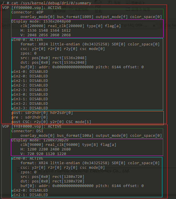
It should be noted that this command depends on the kernel’s debugfs function. If the kernel does not enable the debugfs function or the system does not mount the debugfs node, it is necessary to ensure that the kernel enables the CONFIG_DEBUG_FS option and manually mount it through the following command:
mount -t debugfs none /sys/kernel/debug
9.1.2 Parameter Explanation
1. The two red boxes indicate that the vops used by the two display devices are ff900000.vop and ff8f0000.vop respectively;
2. The green part represents the connector information. The two display devices are an eDP screen and a MIPI screen respectively;
3. The pink part is the display mode, from which the specific timing, DCLK, and frame rate can be known. In the above figure, the two devices are an eDP screen with a resolution of 1536x2048p60 and a MIPI screen with a resolution of 1280x720p29 respectively;
4. The blue part is the VOP layer information. The first display device turns on the win0 layer, with a size of 1536x2048 and a format of XRGB. The second display device turns on the win0 layer, with a size of 1280x720 and a format of XRGB. src and dst represent the size and position of the source data and the display. If the sizes of src and dst are inconsistent, the VOP will perform scaling processing, as shown in the following figure:
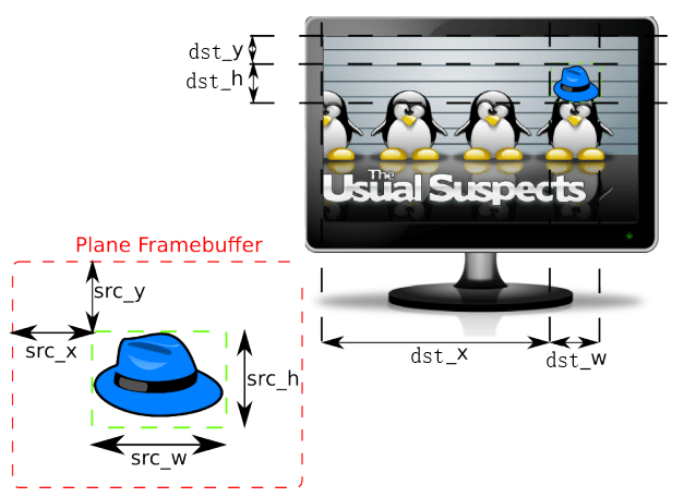
5. The orange part is some status information of VOP HDR and CSC. SDR indicates that the data sent by the application is in SDR format. If it is HDR-format data, the keyword HDR will be seen.
6. The summary information of the VOP2 platform is basically the same as that of the previous platforms, except that the previous VOP is changed to Video Port, and the layer names are changed from the original winx to Cluster-winx or Esmart-winx :
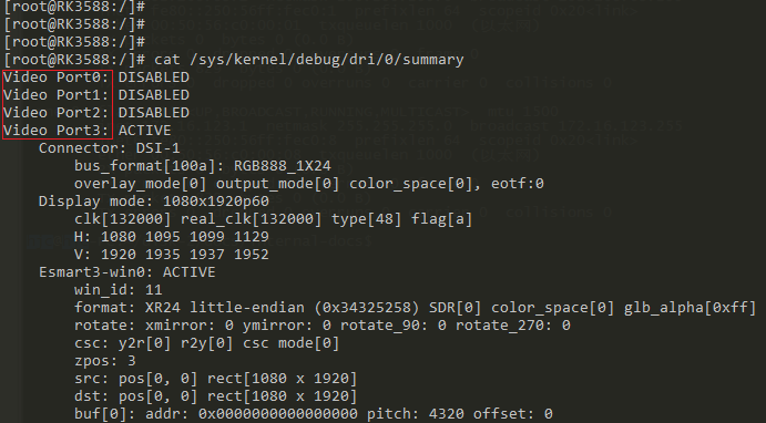
7. Each layer has a format attribute below it. It may be a standard fourcc value such as AB24 , XR24 , NV12 , etc., indicating the format of the data in the framebuffer displayed by this layer. The specific meaning can be referred to drm fourcc.
9.1.3 Dump VOP’s Current Configuration Information
Due to the complex architecture of VOP2 and the large number of register-related configurations, we provide the following two methods to dump the current configuration information of VOP:
1. Obtain the configuration information by catting the DRM device node. For example:
(1) Obtain the register configuration of the working modules in VOP
cat /sys/kernel/debug/dri/0/active_regs
(2) Obtain the register configuration of all sub-modules of VOP
cat /sys/kernel/debug/dri/0/regs
The above two commands can dump the relevant register configurations of VOP. Coupled with cat /sys/kernel/debug/dri/0/summary in the previous chapter, the current display status information of VOP can be basically dumped.
It should be noted that this function is supported by default in the Linux-6.1 and later kernels. In the Linux-5.10 and Linux-
4.19 kernels, it needs to be updated to a relatively new version to be supported. If you are using these two versions of the kernel and it is not convenient to update, you can use method 2 below.
2. Use the vop2_dump.sh script
This script can more conveniently dump the display status information related to vop. Most SDKs come with this script by default. If not, it can be obtained through the following address: vop2_dump.
It should be noted that this script also depends on debugfs and requires the kernel to enable the CONFIG_DEVMEM option to facilitate the script to read the register configuration using the io command.
9.2 Dump the Currently Displayed Buffer
Sometimes, we find that the content displayed on the screen is abnormal. This abnormality may be due to problems in the link from VOP-> display interface-> screen/monitor, or it may be that the display data drawn by the application above is abnormal. At this time, we can dump the data of the buffer displayed by the VOP layer and then use software such as 7yuv to check whether these data are normal. If these data are abnormal themselves, it means that the data sent from the userspace are problematic. Otherwise, the display path from VOP to the screen needs to be checked.
9.2.1 Usage Instructions
First, it is necessary to ensure that the Linux kernel make menuconfig enables the CONFIG_ROCKCHIP_DRM_DEBUG option.
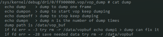
1. Dump one frame of the currently displayed buffer
echo dump > /sys/kernel/debug/dri/0/**ff900000.vop**/vop_dump/dump
2. Continuously dump n frames of the displayed buffer
echo dumpn > /sys/kernel/debug/dri/0/**ff900000.vop**/vop_dump/dump
3. The dumped files are saved in /data/vop_buf/ , and can be viewed using 7yuv software.
4. The bold part [ff900000.vop] in the above path is different on different platforms. The specific path can correspond to the VOP/Video Port of the cat /sys/kernel/debug/dri/0/summary node. For example, for RK3588, the path will become: /sys/kernel/debug/dri/0/video_port0/dump
9.3 Use the VP Self-test Mode to Display Color Bars
On platforms using the VOP2 architecture, each VP supports displaying color bars in the self-test mode. Taking VP0 as an example, the commands are as follows:
Enable horizontal color bar:
  echo 1 > /sys/kernel/debug/dri/0/video_port0/color_bar
Enable vertical color bar:
  echo 2 > /sys/kernel/debug/dri/0/video_port0/color_bar
Disable color bar:
  echo 0 > /sys/kernel/debug/dri/0/video_port0/color_bar
1. Display effect when color_bar is set to 1
2. Display effect when color_bar is set to 2

For scenarios where the screen cannot be displayed or the display is abnormal in products, the VP self-test mode can be used for debugging according to the following process:
-
If the VP self-test mode can display color bars normally, it can be excluded that there are abnormalities in the display interface and the screen-end. The focus should be on whether there are abnormalities in VOP and the userspace;
-
If the VP self-test mode cannot display color bars normally, the focus should be on the possible abnormalities in VOP and the modules after VOP.
9.4 Adjust the DRM Print Log Level to Capture Logs
DRM sets the following print levels according to different interfaces. The print of which interface to turn on or off can be determined through the DRM debug node. For example, if you want to view the print of ATOMIC, you can enter the command:
echo 0x10 > /sys/module/drm/parameters/debug
If you want to see all the debugging information, you can enter the command:
echo 0xff > /sys/module/drm/parameters/debug
Among them, bit 5 of 0x20 corresponds to vsync-related information. The printed content is very large. If this information is not concerned during debugging, this bit is generally not set.
For more print levels, you can view the following definition:
Enable debug output, where each bit enables a debug category.
Bit 0 (0x01) will enable CORE messages (drm core code)
Bit 1 (0x02) will enable DRIVER messages (drm controller code)
Bit 2 (0x04) will enable KMS messages (modesetting code)
Bit 3 (0x08) will enable PRIME messages (prime code)
Bit 4 (0x10) will enable ATOMIC messages (atomic code)
Bit 5 (0x20) will enable VBL messages (vblank code)
Bit 7 (0x80) will enable LEASE messages (leasing code)
Bit 8 (0x100) will enable DP messages (displayport code)
There is a lot of printing here, and by default, it is not printed to the serial port. Therefore, after turning on the corresponding debugging switch, only part of the debugging information will be seen in the serial port terminal by default. To obtain the complete log information, the dmesg command needs to be used for viewing.
9.5 View the Current Display Clock
The clock is one of the key factors affecting the display module. Therefore, we often need to obtain the current system-provided clock. It can be obtained through the following commands:
1. Obtain the entire clock tree
cat /sys/kernel/debug/clk/clk_summary
2. If only focusing on the VOP clock
cat /sys/kernel/debug/clk/clk_summary | grep vop
For display interfaces such as HDMI/DP/VGA/CVBS, the DCLK corresponding to each resolution has strict standard requirements. If the DCLK clock is incorrect, there may be problems such as inability to display or display compatibility issues. For display interfaces such as eDP/LVDS/MIPI/RGB, there is generally a certain margin.
When the VOP2 driver enables the corresponding display interface, there will be the following print, showing the clock frequency required by the display interface and the clock frequency obtained from the system. Special attention should be paid when the two do not match.
rockchip-vop2: [vop2_crtc_atomic_enable] Update mode to 3840x2160p60, type: 10(if:200) for vp2 dclk: 533280000
fdd90000.vop: [drm:vop2_crtc_atomic_enable] dclk_out2 div: 2 dclk_core2 div: 2
fdd90000.vop: [drm:vop2_crtc_atomic_enable] set dclk_vop2 to 533280000, get 533279987
This log shows that a DP interface (judged by type) is being enabled on VP2, displaying a 4K resolution. The required dclk is 533280000 HZ, but the system-allocated value is 533279987 HZ. Since DP has very high requirements for the accuracy of dclk, in this case, the screen is most likely not to light up.
9.6 Force-turn on/off the Display Device
Taking LVDS as an example:
Turn off LVDS: echo off > /sys/class/drm/card0-LVDS-1/status
Turn on LVDS: echo on > /sys/class/drm/card0-LVDS-1/status
9.7 View the Usage of DRM Buffer
The usage of the buffer applied through DRM GEM can be known through the following command:
cat /sys/kernel/debug/dri/0/mm_dump

9.8 View the GPIO State
During the initial bring-up and screen-lighting stage of the project, it is often necessary to control the power of the screen or backlight by controlling the state of the GPIO. We can confirm whether the GPIO state configured by the software is correct through the following command:
cat /sys/kernel/debug/gpio
9.9 Usage of modetest
modetest is a command-line tool integrated in libdrm for testing the drm system. It can provide the following functions:
1. Dump the basic state of the drm system
[root@RK356X:/]# modetest -M rockchip
Encoders:
id   crtc type possible crtcs possible clones
151  0   Virtual 0x00000007 0x00000000
153  0   TMDS 0x00000002 0x00000000
155  71  TMDS 0x00000001 0x00000000
166  0   DPI  0x00000004 0x00000000
Connectors:
id   encoder status name     size (mm) modes encoders
154  0    disconnected eDP-1 0x0       0    153
 props:
     1 EDID:
          flags: immutable blob
          blobs:
          value:
     2 DPMS:
          flags: enum
          enums: On=0 Standby=1 Suspend=2 Off=3
          value: 0
156  155  connected HDMI-A-1 530x300   31   155
 modes:
     name refresh (Hz) hdisp hss hse htot vdisp vss vse vtot)
 1920x1080 60 1920 2008 2052 2200 1080 1084 1089 1125 148500 flags: phsync, pvsync; type: preferred, driver
 1920x1080 60 1920 2008 2052 2200 1080 1084 1089 1125 148352 flags: phsync, pvsync; type: driver
 1920x1080 50 1920 2448 2492 2640 1080 1084 1089 1125 148500 flags: phsync, pvsync; type: driver
 1280x720 60 1280 1390 1430 1650 720 725 730 750 74250 flags: phsync, pvsync; type: driver
 720x576 50 720 732 796 864 576 581 586 625 27000 flags: nhsync, nvsync; type: driver
 720x480 60 720 736 798 858 480 489 495 525 27027 flags: nhsync, nvsync; type: driver
 props:
167  0    disconnected HDMI-A-2 0x0    0    166
 props:
CRTCs:
id   fb   pos  size
71   0    (0,0) (1920x1080)
  60 1920 2008 2052 2200 1080 1084 1089 1125 148500 flags: phsync, pvsync; type: userdef
 props:
     72 PLANE_MASK:
          flags: immutable bitmask
          values: Cluster0=0x1 Cluster1=0x2 Esmart0=0x4 Esmart1=0x8 Smart0=0x10 Smart1=0x20 Cluster2=0x40 Cluster3=0x80 Esmart2=0x100 Esmart3=0x200
          value: 21
     26 GAMMA_LUT:
          flags: blob
          blobs:
          value:
     27 GAMMA_LUT_SIZE:
          flags: immutable range
          values: 0 4294967295
          value: 1024
87   0    (0,0) (0x0)
  0 0 0 0 0 0 0 0 0 0 flags: ; type:
 props:
     88 PLANE_MASK:
          flags: immutable bitmask
          values: Cluster0=0x1 Cluster1=0x2 Esmart0=0x4 Esmart1=0x8 Smart0=0x10 Smart1=0x20 Cluster2=0x40 Cluster3=0x80 Esmart2=0x100 Esmart3=0x200
          value: 34
     26 GAMMA_LUT:
          flags: blob
          blobs:
          value:
     27 GAMMA_LUT_SIZE:
          flags: immutable range
          values: 0 4294967295
          value: 1024
103  0    (0,0) (0x0)
  0 0 0 0 0 0 0 0 0 0 flags: ; type:
 props:
     104 PLANE_MASK:
          flags: immutable bitmask
          values: Cluster0=0x1 Cluster1=0x2 Esmart0=0x4 Esmart1=0x8 Smart0=0x10 Smart1=0x20 Cluster2=0x40 Cluster3=0x80 Esmart2=0x100 Esmart3=0x200
          value: 8
     26 GAMMA_LUT:
          flags: blob
          blobs:
          value:
     27 GAMMA_LUT_SIZE:
          flags: immutable range
          values: 0 4294967295
          value: 1024
Planes:
id   crtc fb   CRTC x,y x,y  gamma size possible crtcs
57   0    0    0,0      0,0  0         0x00000007
 formats: XR24 AR24 XB24 AB24 RG24 BG24 RG16 BG16
 props:
     8 type:
          flags: immutable enum
          enums: Overlay=0 Primary=1 Cursor=2
          value: 1
     60 alpha:
          flags: range
          values: 0 65535
          value: 65535
     61 pixel blend mode:
          flags: enum
          enums: None=2 Pre-multiplied=0 Coverage=1
          value: 0
     62 zpos:
          flags: range
          values: 0 7
          value: 0
     63 NAME:
          flags: immutable bitmask
          values: Smart0-win0=0x1
          value: 1
     70 colorkey:
          flags: range
          values: 0 2164260863
          value: 0
73   0    0    0,0      0,0  0         0x00000007
 formats: XR24 AR24 XB24 AB24 RG24 BG24 RG16 BG16
 props:
     8 type:
          flags: immutable enum
          enums: Overlay=0 Primary=1 Cursor=2
          value: 1
     76 alpha:
          flags: range
          values: 0 65535
          value: 65535
     77 pixel blend mode:
          flags: enum
          enums: None=2 Pre-multiplied=0 Coverage=1
          value: 0
     78 zpos:
          flags: range
          values: 0 7
          value: 1
     79 NAME:
          flags: immutable bitmask
          values: Smart1-win0=0x2
         value: 2
     86 colorkey:
         flags: range
         values: 0 2164260863
         value: 0
89   0   0    0,0       0,0  0        0x00000007
 formats: XR24 AR24 XB24 AB24 RG24 BG24 RG16 BG16 NV12 NV16 NV24 NA12 NA16 NA24 YVYU VYUY
 props:
     8 type:
         flags: immutable enum
         enums: Overlay=0 Primary=1 Cursor=2
         value: 1
     92 alpha:
         flags: range
         values: 0 65535
         value: 65535
     93 pixel blend mode:
         flags: enum
         enums: None=2 Pre-multiplied=0 Coverage=1
         value: 0
     94 zpos:
         flags: range
         values: 0 7
         value: 2
     95 NAME:
         flags: immutable bitmask
         values: Esmart1-win0=0x4
         value: 4
105  0   0    0,0       0,0  0        0x00000007
 formats: XR24 AR24 XB24 AB24 RG24 BG24 RG16 BG16 NV12 NV16 NV24 NA12 NA16 NA24 YVYU VYUY
 props:
     8 type:
         flags: immutable enum
         enums: Overlay=0 Primary=1 Cursor=2
         value: 0
     108 alpha:
         flags: range
         values: 0 65535
         value: 65535
     109 pixel blend mode:
         flags: enum
         enums: None=2 Pre-multiplied=0 Coverage=1
         value: 0
     110 zpos:
         flags: range
         values: 0 7
         value: 3
     111 NAME:
         flags: immutable bitmask
         values: Esmart0-win0=0x8
         value: 8
The first part of the Encoders output corresponds to the second part of the Connectors. From the Dump output, we can see that: The Connectore eDP-1 has an id of 154, its corresponding Encoder id is 153, and it is in the disconnected state, indicating that the underlying driver has not detected the connection of this eDP device. The possible crtcs value of Encoder 153 is 2, i.e., BIT(1), which is a bit-wise AND mask, indicating that this eDP can only be connected to VP1.
The Connector HDMI-A-1 has an id of 156, its corresponding Encoder id is 155, and it is in the connected state, indicating that the underlying driver has detected that a display device is connected to this HDMI interface. The modes are the resolutions supported by the corresponding display device reported by the driver. CRTC corresponds to the Video Port in VOP 2.0 or vop in VOP 1.0. Planes correspond to the layers. The listed information includes which VPs the layer can switch between (possible crtcs) and the supported formats (formats). 2. Output color bars of various colors on the corresponding display interface. This function can be used to simply verify the Drm driver.
modetest -M rockchip -s 156@71:1920x1080
Through the above command, smpte color bars similar to the following can be displayed on HDMI-A-1, where 156 is the id of HDMI-A-1 and 71 is the id of VP0.
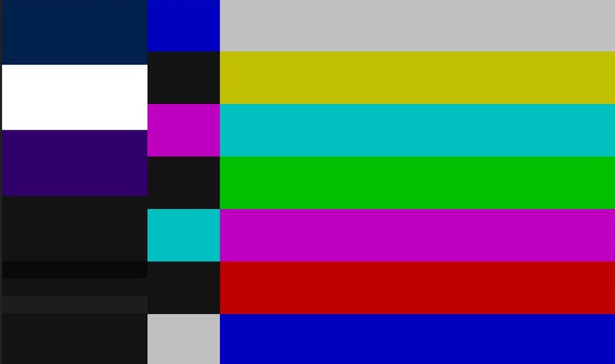
3. Temporarily modify the values of some drm attributes manually
For more usage methods, you can refer to the following usage instructions:
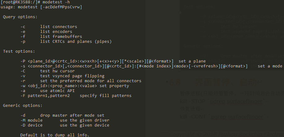
It should be noted that modetest specifies Drm resources such as plane, crtc, and connector by id. These ids can be queried through modetest or through the following command:
cat /sys/kernel/debug/dri/0/state
9.10 Usage of xrandr
xrandr is a display configuration tool on the graphics system using Xserver. It can be used to dump the system’s display information and also to configure the system’s display output.
root@linaro-alip:/# xrandr
Screen 0: minimum 320 x 200, current 1920 x 2048, maximum 8192 x 8192
eDP-1 connected primary 1536x2048+0+0 (normal left inverted right x axis y axis) 0mm x 0mm
  1536x2048 59.99*+
HDMI-1 connected 1920x1080+0+0 (normal left inverted right x axis y axis) 708mm x 398mm
  1920x1080 60.00*+ 50.00 59.94 30.00 24.00 29.97 23.98
  1920x1080i 60.00 50.00 59.94
  1280x1024 60.02
  1440x900 59.90
  1360x768 60.02
  1280x720 60.00 50.00 59.94
  1024x768 60.00
  800x600 60.32
  720x576 50.00
  720x576i 50.00
  720x480 60.00 59.94
  720x480i 60.00 59.94
  640x480 60.00 59.94
DP-1 disconnected (normal left inverted right x axis y axis)
This tool is a general-purpose tool in the Xserver environment. For a detailed usage introduction, please refer to Xrandr
9.11 Pause and Start the Display Process
Sometimes, for the convenience of debugging, we hope that the application stops at a fixed scene. We can use the following commands to pause and resume the display process.
For the Android Surfaceflinger process:
1. Pause the process
kill -STOP `pgrep surfaceflinger`
2. Resume the process
kill -CONT `pgrep surfaceflinger`
For the Linux weston process:
1. Pause the process
Kill -STOP `pgrep weston`
2. Resume the process
kill -CONT `pgrep weston`
For the Linux Xserver process:
1. Pause the process
Kill -STOP `pgrep Xorg`
2. Resume the process
kill -CONT `pgrep Xorg`
In the daily development process, when we hope to temporarily modify some register configurations of the VOP through the io command to view a certain display effect, we should pay special attention to using similar commands to stop the corresponding display main process in the userspace in advance. Otherwise, the update of the display process will overwrite the local register modifications at any time.
9.12 Obtain EDID Information
Taking HDMI as an example:
cat /sys/class/drm/card0-HDMI-A-1/edid > /data/edid.bin
9.13 View HDMI Status
cat /sys/kernel/debug/dw-hdmi/status

10. FAQ
10.1 VOP POST_BUF_EMPTY
There may be a log similar to the following:
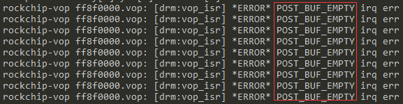
Possible reasons are as follows:
1. Insufficient bandwidth
If the system bandwidth is insufficient, the VOP cannot obtain data in a timely manner, resulting in a post buf empty error. The following attempts can be made:
(1) Try to fix the ddr to the highest frequency; (2) Lengthen the blanking period of the screen to increase the data-fetching time per line;
2. iommu error
Confirm whether there is an iommu pagefault error as shown in the following figure. If so, try updating to the latest code for testing first. If the problem still exists in the latest code, please submit a remine system and attach the relevant log;
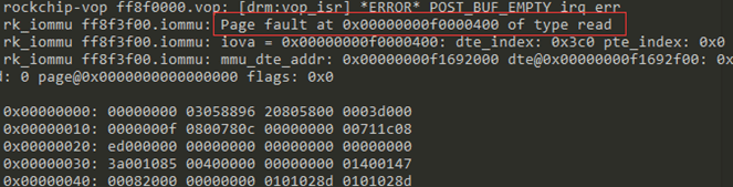
3. Logic voltage is too low
If the Logic voltage is too low, it will cause VOP abnormalities. You can try increasing it by 100mv for testing;
4. AFBDC/IFBDC alignment requirements
For platforms such as PX30/RK3326, RK3368, RK3399, RK356X, and RK3588, if the screen resolution is not 16-pixel-aligned, you can try to turn off the afbdc/ifbdc function. The modification method refers to Chapter 1.3.1 of the document 《FAQ- DRM-HWC》.
10.2 Display Effect Adjustment
The BCSH module inside the VOP supports the adjustment of brightness, contrast, saturation, and chroma. It can be adjusted by configuring the corresponding attributes under the connector through modetest. For the Android system, there is an implementation of attribute configuration based on the Android system. The default value is 50, and N is incremented by 1 each time.
Before Android 9.0, use the commands:
setprop persist.sys.brightness.main val
setprop persist.sys.contrast.main val
setprop persist.sys.saturation.main val
setprop persist.sys.hue.main val
setprop sys.display.timeline N+1
After Android 9.0, use the commands:
setprop persist.vendor.brightness.main val
setprop persist.vendor.contrast.main val
setprop persist.vendor.saturation.main val
setprop persist.vendor.hue.main val
setprop vendor.display.timeline N+1
Starting from Android 11, the SDK has integrated a complete set of display effect adjustment tools and documents. You can refer to the following document description in the Android SDK:
RKDocs/common/display/Rockchip_Introduction_Display_Adjust_APK_CN.pdf
10.3 Screen Fails to Light Up / Abnormal Display after Hibernation Wake-up / No- display Problem
Make further confirmations in the following aspects:
-
Confirm whether there is backlight;
-
Confirm whether the power supply and reset control of the screen are normal;
-
Confirm whether the power-on and power-off timings meet the screen’s spec requirements;
10.4 How to Enable Display Function for RK3308/RV1106/RV1103
Due to the lightweight design concept of RK3308/RV1106/RV1103, they support relatively small memory, so the display function is not supported by default. If the display needs to be enabled, the following configurations are required:
1. U-Boot Modification
RK3308 U-Boot RGB/MCU interface display reference configuration rk3308-display.config:
make rk3308_defconfig rk3308-display.config &&./make.sh
RV1106/RV1103 U-Boot RGB/MCU interface display reference configuration rv1106-display.config:
make rv1106_defconfig rv1106-display.config &&./make.sh
2. Kernel Modification
RK3308 VOP does not support IOMMU, so memory allocation needs to be from the reserved cma buffer. The default CMA_SIZE is 16M. If memory allocation fails, you can refer to the following method to modify CMA_SIZE:
@@ -784,7 +786,12 @@ CONFIG_ARCH_SUPPORTS_MEMORY_FAILURE=y
# CONFIG_MEMORY_FAILURE is not set
# CONFIG_TRANSPARENT_HUGEPAGE is not set
# CONFIG_CLEANCACHE is not set
-# CONFIG_CMA is not set
+CONFIG_CMA=y
+# CONFIG_CMA_INACTIVE is not set
+# CONFIG_CMA_DEBUG is not set
+# CONFIG_CMA_DEBUGFS is not set
+# CONFIG_CMA_SYSFS is not set
+CONFIG_CMA_AREAS=7
# CONFIG_ZPOOL is not set
# CONFIG_ZBUD is not set
# CONFIG_ZSMALLOC is not set
@@ -4917,6 +4925,18 @@ CONFIG_DMA_NONCOHERENT_MMAP=y
CONFIG_DMA_COHERENT_POOL=y
CONFIG_DMA_REMAP=y
CONFIG_DMA_DIRECT_REMAP=y
+CONFIG_DMA_CMA=y
+# CONFIG_DMA_PERNUMA_CMA is not set
+
+#
+# Default contiguous memory area size:
+#
+CONFIG_CMA_SIZE_MBYTES=32
+CONFIG_CMA_SIZE_SEL_MBYTES=y
+# CONFIG_CMA_SIZE_SEL_PERCENTAGE is not set
+# CONFIG_CMA_SIZE_SEL_MIN is not set
+# CONFIG_CMA_SIZE_SEL_MAX is not set
+CONFIG_CMA_ALIGNMENT=8
# CONFIG_DMA_API_DEBUG is not set
CONFIG_SGL_ALLOC=y
CONFIG_CPU_RMAP=y
RK3308 kernel RGB to MIPI display (bridge chip RK618) reference configuration rk3308bs_mipi_display.config:
make ARCH=arm64 rk3308_linux_defconfig rk3308bs_mipi_display.config
RV1106/RV1103 kernel RGB/MCU interface display reference configuration rv1106-evb.config:
make ARCH=arm rv1106_defconfig rv1106-evb.config
10.5 Method to Turn off iommu
After turning off the vop iommu, the memory applied through DRM will be allocated from the CMA memory. The system’s default CMA memory size is 16M. It needs to be adjusted to the corresponding size according to the scene requirements; otherwise, memory allocation may fail.
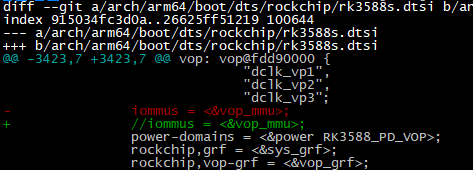
10.6 Application Reference Documents for Various Interfaces
| Module | Document |
|---|---|
| RGB/MCU | Rockchip_Developer_Guide_RGB_MCU_CN.pdf |
| BT656/BT1120 | Rockchip_Developer_Guide_BT656_TX_AND_BT1120_TX_CN.pdf |
| LVDS | Rockchip_Developer_Guide_LVDS_CN.pdf |
| MIPI DSI | Rockchip_Developer_Guide_MIPI_DSI2_CN.pdf |
| eDP | Rockchip_Developer_Guide_eDP_CN.pdf |
| DP | Rockchip_Developer_Guide_DisplayPort_CN.pdf |
| HDMI | Rockchip_Developer_Guide_HDMI_CN.pdf |
10.7 RGB/MCU Screen Frame Rate Calculation Problem
Given:
htotal = hactive + hback-porch + hfront-porch + hsync-len
vtotal = vactive + vback-porch + vfront-porch + vsync-len
N is the number of cycles required to send one pixel:
| bus_format | One Pixel need N Cycle to send |
|---|---|
| MEDIA_BUS_FMT_RGB888_1X24 MEDIA_BUS_FMT_RGB666_1X18 MEDIA_BUS_FMT_RGB565_1X16 |
1 |
| MEDIA_BUS_FMT_RGB888_3X8 | 3 |
| MEDIA_BUS_FMT_RGB888_DUMMY_4X8 | 4 |
Based on the above information, the frame rate can be calculated as follows:
| Interface Type | Frame Rate Calculation |
|---|---|
| RGB | fps = dclk / (htotal x vtotal x N) |
| MCU | fps = dclk / (htotal x vtotal x (mcu-pix-total + 1) x N) |
10.8 How to Write a Driver for a Third-party Conversion Chip
For some third-party conversion chips that require software drivers, we need to use the DRM framework bridge interface to register the connector to the framework. Taking the RGB2HDMI SII902X as an example, at this time, rockchip_rgb.c acts as the encoder, and sii902x.c acts as the connector. Specifically, you can refer to the implementation of the SII902X driver:
drivers/gpu/drm/bridge/sii902x.c
10.9 How Many Slices Does RK3588 DSC Support and What is the Maximum Supported slice width?
RK3588 has 2 DSCs. HDMI0 and DSI0 use DSC0 (DSC_8K), which can support the number of slices: 1, 2, 4, 8. The corresponding slice widths are xres / 1, xres / 2, xres / 4, xres / 8. The maximum width that DSC_8K can support is 7680, so the maximum slice_width is also 7680. HDMI1 and DSI1 use DSC1 (DSC_4K), which can support the number of slices: 1, 2. The corresponding slice widths are xres / 1, xres / 2. The maximum width that DSC_4K can support is 4096, so the maximum slice_width is also 4096.
10.10 Requirements for aclk for Resolutions Higher than 4kP60
For platforms like RK3588 that support resolutions higher than 4KP60 (such as 4KP120, 8KP30, 8KP60, etc.), the default 500M aclk cannot meet the requirements of these resolutions. Therefore, the aclk frequency needs to be set to 800M in the DTS. Otherwise, horizontal stripes may appear on the display due to insufficient VOP performance. The modification method is as follows:
&vop {
  assigned-clocks = <&cru ACLK_VOP>;
  assigned-clock-rates = <800000000>;
};
10.11 How to Enable the Display Mirror Function by Default
In some projects, due to inconsistent molds and screen orientations, it may be desired to mirror the display content by default in software.
The default Y-direction mirror display is not supported. The default X-direction mirror display is only supported by VOP V2.0 and above versions (see the 《Basic VOP Features of Each Platform》 chapter for details). The configuration method is exemplified as follows:
&vp1 {
  xmirror-enable;
};
10.12 Problem of Small-resolution Screens on RV1106/RV1103 Failing to Light Up / Abnormal Display
For the RV1106 and RV1103 platforms, the clock source of dclk_vop can be GPLL or CPLL. Their default frequencies are 1188000 KHz and 1000000 KHz respectively. The CRU module is designed such that the maximum frequency-division coefficient of dclk_vop supported is 32:
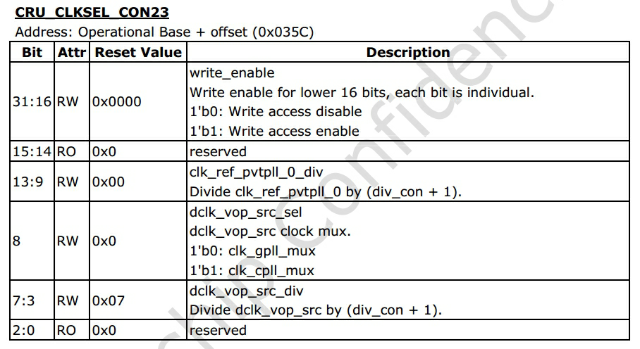
Therefore, the minimum frequencies of dclk_vop under the two PLLs are 37125 KHz and 31250 KHz by default. If the pixel clock of the resolution supported by the screen is less than the above frequencies, it may lead to problems such as failure to light up or abnormal display. If it is necessary to support a display device with a smaller resolution (for example, a resolution of 720x480p60/720x576p60 with a pixel clock of 27000 KHz), only by modifying the frequency of the clock source GPLL or CPLL can the minimum frequency supported by dclk_vop be reduced:
&vop {
  assigned-clocks = <&cru PLL_GPLL>;
  assigned-clock-rates = <594000000>;
};
It should be noted that:
RGB/MCU screens can generally support a certain range of clock frequencies (corresponding to the MIN/TYP/MAX clock rate
specified in the datasheet). If the minimum frequency of dclk_vop under the default GPLL/CPLL can meet the requirement of the MAX clock rate, it is recommended not to modify the frequency of the clock source GPLL/CPLL as much as possible. GPLL and CPLL are usually used as the clock sources for multiple modules. It is necessary to confirm whether the modification of the clock source frequency will affect other modules besides VOP according to the specific application scenario.
11. How to More Efficiently Locate Problems
In daily development, if a Bug or issue is found, scientific analysis and communication can help solve and converge the problem more quickly. For display-related problems, we recommend that developers make the following confirmations after finding the problem.
-
Check the kernel log or application-layer log to see if there are obvious abnormal prompts.
-
If an abnormal log prompt in the kernel is found, search the kernel driver according to the log, and find the relevant code to see what judgment logic is used to output these abnormal logs.
-
Confirm whether the problem is probabilistic or reproducible.
-
For devices such as HDMI and DP that support multiple resolutions, confirm whether the abnormality occurs only at a specific resolution or at all resolutions, and confirm whether the problem occurs only on a specific display or on all displays.
-
If it is an HDMI or DP compatibility-related problem, under the premise of controlling variables, find a third-party device for comparison to see how the third-party device behaves under the same conditions.
-
If the abnormality occurs in the video-playing scenario, confirm whether the problem occurs only with specific videos or apps, or with any video or app.
-
If no direction can be found, confirm whether this abnormality has always existed or only occurred after updating specific code or version. If it is the latter, use the binary search method and the control-variable method to find out which version or module was updated before the abnormality occurred.
12. Reference Documents
-
Rockchip_drm_integration_helper-zh.pdf
-
Rockchip_DRM_Panel_Porting_Guide.pdf
-
Rockchip_Developer_Guide_HDMI_CN.pdf
-
RK3588_MIPI_DSI2_Developer_Guide_CN.pdf
-
Rockchip_BT656_TX_AND_BT1120_TX_Developer_Guide_CN.pdf
-
Rockchip RK3568 Datasheet.pdf
-
Rockchip rk fb development guide.pdf
-
Wikipedia for Direct_Rendering_Manager
-
Linux DRM Developer’s Guide