
This is a complete adaptation of Rockchip BT.656 TX and BT.1120 TX Developer Guide V2.2.0 (RK-YH-YF-178). Only a Chinese PDF was supplied; English and Russian are full translations. All six source figures come from that PDF: existing English labels in a figure do not imply an English source PDF. Tables are editable, and tables embedded in images retain the original figure alongside copyable data.
This is a Rockchip BSP platform reference, not a promise of support on every ArmSoM board. The source product-version table follows. RK3576 appears in the capability and wiring sections but is absent from this kernel-version table; no kernel version is invented for it. Use this reference with ArmSoM Sige5 (RK3576) or Sige7 (RK3588) only after checking routed pins, carrier hardware, power, receiver, SDK/BSP and kernel driver. No ArmSoM hardware validation has been performed. Examples below are source examples.
| Chip | Kernel version |
|---|---|
| RV1109/RV1126 | Linux kernel 4.19 and later |
| RV1103/RV1106 | Linux kernel 5.10 and later |
| RK356X | Linux kernel 4.19 and later |
| RK3588 | Linux kernel 5.10 and later |
| RK3562 | Linux kernel 5.10 and later |
| RK3506 | Linux kernel 6.1 and later |
| RV1126B | Linux kernel 6.1 and later |
1. Basic concepts
BT.656 and BT.1120 define SDTV and HDTV interfaces respectively. EAV and SAV timing-reference codes carry embedded synchronization during blanking; data uses YCbCr 4:2:2. Some manuals call these video or YUV signals. On the RK platforms described by the source, both image data and timing-reference codes have 8-bit depth. Consult Rec. ITU-R BT.1120 and Rec. ITU-R BT.656 for protocol details.
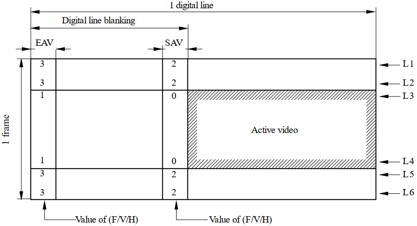
1.1 Progressive (P) scan timing
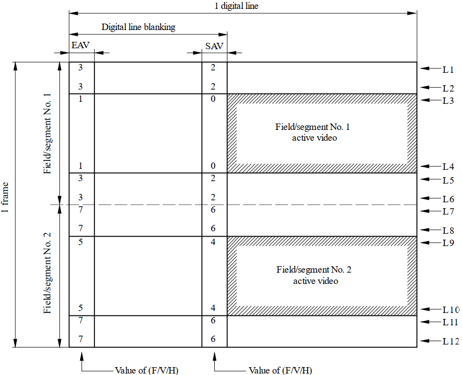
1.2 Interlaced (I) scan timing
1.3 Timing-reference codes
The first three words are fixed at 0xFF, 0x00, 0x00; the fourth depends on scan position. Bit9 is fixed at 1. In Bit8(F), the source describes F=0 as the even field and F=1 as the odd field. Bit7(V) is 0 for a line containing active video and 1 otherwise. Bit6(H) is 0 for SAV and 1 for EAV. Bit[5,2] (P3,P2,P1,P0) is calculated from F/V/H. Bit[1,0] is fixed at 0; for 8-bit RK operation, these two low bits can be regarded as absent.
Bit5 = V XOR H
Bit4 = F XOR H
Bit3 = F XOR V
Bit2 = F XOR V XOR H
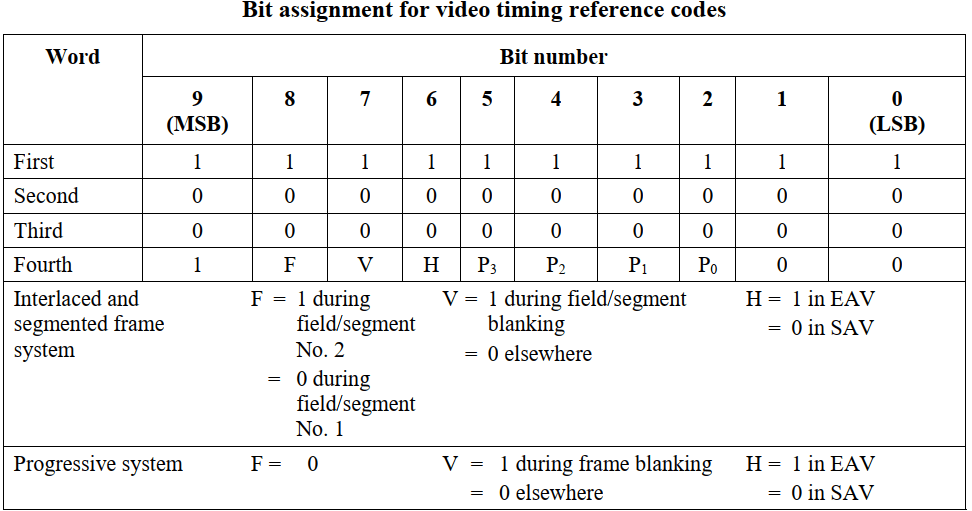
| Word | 9 (MSB) | 8 | 7 | 6 | 5 | 4 | 3 | 2 | 1 | 0 (LSB) |
|---|---|---|---|---|---|---|---|---|---|---|
| 1 | 1 | 1 | 1 | 1 | 1 | 1 | 1 | 1 | 1 | 1 |
| 2 | 0 | 0 | 0 | 0 | 0 | 0 | 0 | 0 | 0 | 0 |
| 3 | 0 | 0 | 0 | 0 | 0 | 0 | 0 | 0 | 0 | 0 |
| 4 | 1 | F | V | H | P3 | P2 | P1 | P0 | 0 | 0 |
The source figure additionally defines F=1 in field/segment 2 and F=0 in field/segment 1 for interlaced/segmented-frame systems. V=1 during field/segment blanking and 0 elsewhere. In progressive systems F=0; V=1 during frame blanking and 0 elsewhere. In both cases H=1 for EAV and H=0 for SAV. Protection bits for each (F,V,H) combination follow.
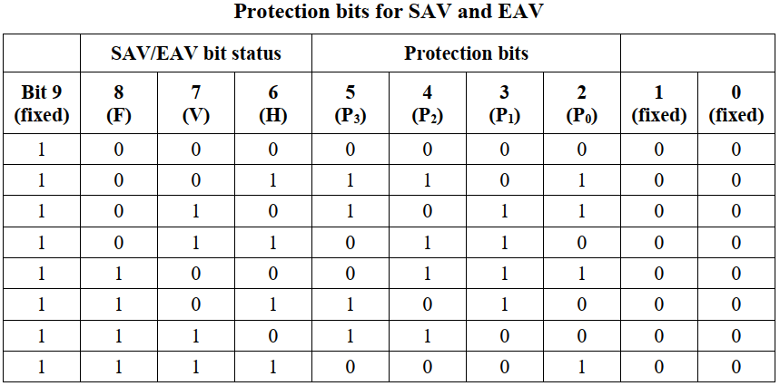
| Bit9 | F | V | H | P3 | P2 | P1 | P0 | Bit1 | Bit0 |
|---|---|---|---|---|---|---|---|---|---|
| 1 | 0 | 0 | 0 | 0 | 0 | 0 | 0 | 0 | 0 |
| 1 | 0 | 0 | 1 | 1 | 1 | 0 | 1 | 0 | 0 |
| 1 | 0 | 1 | 0 | 1 | 0 | 1 | 1 | 0 | 0 |
| 1 | 0 | 1 | 1 | 0 | 1 | 1 | 0 | 0 | 0 |
| 1 | 1 | 0 | 0 | 0 | 1 | 1 | 1 | 0 | 0 |
| 1 | 1 | 0 | 1 | 1 | 0 | 1 | 0 | 0 | 0 |
| 1 | 1 | 1 | 0 | 1 | 1 | 0 | 0 | 0 | 0 |
| 1 | 1 | 1 | 1 | 0 | 0 | 0 | 1 | 0 | 0 |
Combining these definitions gives the following timing-reference codes for blanking intervals:
| EAV | CODE | SAV | CODE |
|---|---|---|---|
| 1 | 0XFF 0X00 0X00 0X9D | 0 | 0XFF 0X00 0X00 0X80 |
| 3 | 0XFF 0X00 0X00 0XB6 | 2 | 0XFF 0X00 0X00 0XAB |
| 5 | 0XFF 0X00 0X00 0XDA | 4 | 0XFF 0X00 0X00 0XC7 |
| 7 | 0XFF 0X00 0X00 0XF1 | 6 | 0XFF 0X00 0X00 0XEC |
2. RK platform support
| SoC platform | BT.656 support | BT.1120 support | Scan modes |
|---|---|---|---|
| RV1109/RV1126 | N | Y | Progressive only |
| RV1103 | Y | N | Progressive and interlaced |
| RV1106 | Y | Y | Progressive and interlaced |
| RK3566/RK3568 | Y | Y | Progressive and interlaced |
| RK3588 | Y | Y | Progressive and interlaced |
| RK3562 | Y | Y | Progressive and interlaced |
| RK3576 | Y | Y | Progressive and interlaced |
| RK3506 | Y | Y | Progressive and interlaced |
| RV1126B | Y | Y | Progressive and interlaced |
3. Hardware connections
3.1 RV1109/RV1126/RV1103/RV1106/RK3566/RK3568/RK3588
Three wiring arrangements are supported below. Set the matching bus_format in DTS or the converter driver according to the actual wiring.

| Interface | Clock | D15 | D14 | D13 | D12 | D11 | D10 | D9 | D8 | D7 | D6 | D5 | D4 | D3 | D2 | D1 | D0 | bus_format |
|---|---|---|---|---|---|---|---|---|---|---|---|---|---|---|---|---|---|---|
| BT.656 | Clock | - | - | - | - | - | - | - | - | D7 | D6 | D5 | D4 | D3 | D2 | D1 | D0 | MEDIA_BUS_FMT_UYVY8_2X8 |
| BT.1120 (1) | Clock | Y7 | Y6 | Y5 | Y4 | Y3 | Y2 | Y1 | Y0 | C7 | C6 | C5 | C4 | C3 | C2 | C1 | C0 | MEDIA_BUS_FMT_YUYV8_1X16 |
| BT.1120 (2) | Clock | C7 | C6 | C5 | C4 | C3 | C2 | C1 | C0 | Y7 | Y6 | Y5 | Y4 | Y3 | Y2 | Y1 | Y0 | MEDIA_BUS_FMT_UYVY8_1X16 |
3.2 RK3562/RK3576/RK3506/RV1126B
BT.656 sends image data to both m0 and m1 pin groups simultaneously, allowing a single display or mirrored dual displays as required.
| Component Name | Pin Name | BT1120 | BT656 |
|---|---|---|---|
| Bus Format | × | MEDIA_BUS_FMT_YUYV8_1X16/ MEDIA_BUS_FMT_UYVY8_1x16 | MEDIA_BUS_FMT_UYVY8_2X8 |
| DCLK | VO_LCDC_CLK | DCLK(RS) | DCLK(RS) |
| R7_D23 | VO_LCDC_D23 | √ | √ (D7_m1) |
| R6_D22 | VO_LCDC_D22 | √ | √ (D6_m1) |
| R5_D21 | VO_LCDC_D21 | √ | √ (D5_m1) |
| R4_D20 | VO_LCDC_D20 | √ | √ (D4_m1) |
| R3_D19 | VO_LCDC_D19 | √ | √ (D3_m1) |
| R2_D18 | VO_LCDC_D18 | × | × |
| R1_D17 | VO_LCDC_D17 | × | × |
| R0_D16 | VO_LCDC_D16 | × | × |
| G7_D15 | VO_LCDC_D15 | √ | √ (D2_m1) |
| G6_D14 | VO_LCDC_D14 | √ | √ (D1_m1) |
| G5_D13 | VO_LCDC_D13 | √ | √ (D0_m1) |
| G4_D12 | VO_LCDC_D12 | √ | √ (D7_m0) |
| G3_D11 | VO_LCDC_D11 | √ | √ (D6_m0) |
| G2_D10 | VO_LCDC_D10 | √ | √ (D5_m0) |
| G1_D9 | VO_LCDC_D9 | × | × |
| G0_D8 | VO_LCDC_D8 | × | × |
| B7_D7 | VO_LCDC_D7 | √ | √ (D4_m0) |
| B6_D6 | VO_LCDC_D6 | √ | √ (D3_m0) |
| B5_D5 | VO_LCDC_D5 | √ | √ (D2_m0) |
| B4_D4 | VO_LCDC_D4 | √ | √ (D1_m0) |
| B3_D3 | VO_LCDC_D3 | √ | √ (D0_m0) |
| B2_D2 | VO_LCDC_D2 | × | × |
| B1_D1 | VO_LCDC_D1 | × | × |
| B0_D0 | VO_LCDC_D0 | × | × |
3.3 RV1126B-P
RV1126B-P introduces data maps to retain compatibility with earlier RV1126 wiring. A data map selects the pins carrying the data. Definitions in include/dt-bindings/display/rockchip_vop.h are:
 /* { 8'd0, BT1120[15:0] } */
 #define ROCKCHIP_BT1120_DATA_MAP_DATA_PADLO 0
 /* { BT1120[15:0], 8'd0 }*/

 #define ROCKCHIP_BT1120_DATA_MAP_DATA_PADHI 1
 /*
  * { BT1120[15:11], 3'd0, BT1120[10:5], 2'd0, BT1120[4:0], 3'b0 }
  * That is:
  *   LCDC_D23 -> BT1120_D15
  *   LCDC_D22 -> BT1120_D14
  *   LCDC_D21 -> BT1120_D13
  *   LCDC_D20 -> BT1120_D12
  *   LCDC_D19 -> BT1120_D11
  *   LCDC_D18 -> N/A
  *   LCDC_D17 -> N/A
  *   LCDC_D16 -> N/A

  *   LCDC_D15 -> BT1120_D10
  *   LCDC_D14 -> BT1120_D9
  *   LCDC_D13 -> BT1120_D8
  *   LCDC_D12 -> BT1120_D7
  *   LCDC_D11 -> BT1120_D6
  *   LCDC_D10 -> BT1120_D5
  *   LCDC_D9 -> N/A
  *   LCDC_D8 -> N/A
  *   LCDC_D7 -> BT1120_D4
  *   LCDC_D6 -> BT1120_D3
  *   LCDC_D5 -> BT1120_D2
  *   LCDC_D4 -> BT1120_D1
  *   LCDC_D3 -> BT1120_D0

  *   LCDC_D2 -> N/A
  *   LCDC_D1 -> N/A
  *   LCDC_D0 -> N/A
  */
 #define ROCKCHIP_BT1120_DATA_MAP_DATA_WITH_DUMMY_0 3
 /* { 16'd0, BT656[7:0] }*/
 #define ROCKCHIP_BT656_DATA_MAP_PADLO 0
 /* { 8'd0, BT656[7:0], 8'd0 }*/
 #define ROCKCHIP_BT656_DATA_MAP_DUMMY_HI_LO 1
 /* { BT656[7:0], 16'd0 }*/
 #define ROCKCHIP_BT656_DATA_MAP_PADHI 2
 /*

  * { BT656[7:3], 3'd0, BT656[2:0], BT656[7:5], 2'd0, BT656[4:0], 3'd0 }
  * That is:
  *   LCDC_D23 -> BT656_D7_M1
  *   LCDC_D22 -> BT656_D6_M1
  *   LCDC_D21 -> BT656_D5_M1
  *   LCDC_D20 -> BT656_D4_M1
  *   LCDC_D19 -> BT656_D3_M1
  *   LCDC_D18 -> N/A
  *   LCDC_D17 -> N/A
  *   LCDC_D16 -> N/A
  *   LCDC_D15 -> BT656_D2_M1
  *   LCDC_D14 -> BT656_D1_M1
  *   LCDC_D13 -> BT656_D0_M1
  *   LCDC_D12 -> BT656_D7_M0
  *   LCDC_D11 -> BT656_D6_M0
  *   LCDC_D10 -> BT656_D5_M0

  *   LCDC_D9 -> N/A
  *   LCDC_D8 -> N/A
  *   LCDC_D7 -> BT656_D4_M0
  *   LCDC_D6 -> BT656_D3_M0
  *   LCDC_D5 -> BT656_D2_M0
  *   LCDC_D4 -> BT656_D1_M0
  *   LCDC_D3 -> BT656_D0_M0
  *   LCDC_D2 -> N/A
  *   LCDC_D1 -> N/A
  *   LCDC_D0 -> N/A
  */
 #define ROCKCHIP_BT656_DATA_MAP_DATA_WITH_DUMMY_0 3
RV1126B default wiring corresponds to ROCKCHIP_BT1120_DATA_MAP_DATA_WITH_DUMMY_0 and ROCKCHIP_BT656_DATA_MAP_DATA_WITH_DUMMY_0, respectively, as shown below.
| Component Name | Pin Name | BT1120 | BT656 |
|---|---|---|---|
| Bus Format | × | MEDIA_BUS_FMT_YUYV8_1X16/ MEDIA_BUS_FMT_UYVY8_1x16 | MEDIA_BUS_FMT_UYVY8_2X8 |
| DCLK | VO_LCDC_CLK | DCLK(RS) | DCLK(RS) |
| R7_D23 | VO_LCDC_D23 | √ | √ (D7_m1) |
| R6_D22 | VO_LCDC_D22 | √ | √ (D6_m1) |
| R5_D21 | VO_LCDC_D21 | √ | √ (D5_m1) |
| R4_D20 | VO_LCDC_D20 | √ | √ (D4_m1) |
| R3_D19 | VO_LCDC_D19 | √ | √ (D3_m1) |
| R2_D18 | VO_LCDC_D18 | × | × |
| R1_D17 | VO_LCDC_D17 | × | × |
| R0_D16 | VO_LCDC_D16 | × | × |
| G7_D15 | VO_LCDC_D15 | √ | √ (D2_m1) |
| G6_D14 | VO_LCDC_D14 | √ | √ (D1_m1) |
| G5_D13 | VO_LCDC_D13 | √ | √ (D0_m1) |
| G4_D12 | VO_LCDC_D12 | √ | √ (D7_m0) |
| G3_D11 | VO_LCDC_D11 | √ | √ (D6_m0) |
| G2_D10 | VO_LCDC_D10 | √ | √ (D5_m0) |
| G1_D9 | VO_LCDC_D9 | × | × |
| G0_D8 | VO_LCDC_D8 | × | × |
| B7_D7 | VO_LCDC_D7 | √ | √ (D4_m0) |
| B6_D6 | VO_LCDC_D6 | √ | √ (D3_m0) |
| B5_D5 | VO_LCDC_D5 | √ | √ (D2_m0) |
| B4_D4 | VO_LCDC_D4 | √ | √ (D1_m0) |
| B3_D3 | VO_LCDC_D3 | √ | √ (D0_m0) |
| B2_D2 | VO_LCDC_D2 | × | × |
| B1_D1 | VO_LCDC_D1 | × | × |
| B0_D0 | VO_LCDC_D0 | × | × |
To match earlier RV1126 wiring, RV1126B-P defaults to ROCKCHIP_BT1120_DATA_MAP_DATA_PADLO for BT.1120 and ROCKCHIP_BT656_DATA_MAP_PADLO for BT.656. Connections follow.

| Interface | Clock | D15 | D14 | D13 | D12 | D11 | D10 | D9 | D8 | D7 | D6 | D5 | D4 | D3 | D2 | D1 | D0 | bus_format |
|---|---|---|---|---|---|---|---|---|---|---|---|---|---|---|---|---|---|---|
| BT.656 | Clock | - | - | - | - | - | - | - | - | D7 | D6 | D5 | D4 | D3 | D2 | D1 | D0 | MEDIA_BUS_FMT_UYVY8_2X8 |
| BT.1120 (1) | Clock | Y7 | Y6 | Y5 | Y4 | Y3 | Y2 | Y1 | Y0 | C7 | C6 | C5 | C4 | C3 | C2 | C1 | C0 | MEDIA_BUS_FMT_YUYV8_1X16 |
| BT.1120 (2) | Clock | C7 | C6 | C5 | C4 | C3 | C2 | C1 | C0 | Y7 | Y6 | Y5 | Y4 | Y3 | Y2 | Y1 | Y0 | MEDIA_BUS_FMT_UYVY8_1X16 |
Both platforms normally have predefined wiring and need no extra setting. If a change is necessary, use DTS. This example makes RV1126B use earlier RV1126 wiring; it is already the default on RV1126B-P.
 &rgb {
    /*
    * RV1126 compatible pin output mode 0.

    *
    * BT1120: ROCKCHIP_BT1120_DATA_MAP_DATA_PADLO
    * BT656: ROCKCHIP_BT656_DATA_MAP_PADLO
    */
    rockchip,data-map-mode = <0>;
 };
4. Software configuration
4.1 Enabling BT.656/BT.1120
(1) If the receiving device needs no transmitter-side software driver (no DRM connector registration), configure the DTS panel node:
 panel {
    ……

    bus-format = MEDIA_BUS_FMT_YUYV8_1X16; //or
 MEDIA_BUS_FMT_YUYV8_1X16/MEDIA_BUS_FMT_UYVY8_1X16
    ……
 }
(2) If a transmitter-side driver and DRM connector registration are required, use the DTS method above or set the format in the connector driver’s drm_connector_helper_funcs -> get_modes. See drivers/gpu/drm/bridge/sii902x.c:
 static int sii902x_get_modes(struct drm_connector *connector)
 {
    u32 bus_format = MEDIA_BUS_FMT_YUYV8_1X16;//depend on hardware

    ……
    drm_display_info_set_bus_formats(&connector->display_info, &bus_format, 1);
    ……
 }
With bus_format configured by either method, the VOP driver enables BT.656/BT.1120 and sets the corresponding pin mapping.
4.2 Timing configuration
There are three timing-configuration methods. First, for a product with a fixed resolution, configure timing in the DTS panel node. Progressive example:
 timing_1080p: timing-1080p {
    clock-frequency = <148500000>;

    hactive = <1920>;
    vactive = <1080>;
    hback-porch = <100>;
    hfront-porch = <200>;
    vback-porch = <10>;
    vfront-porch = <10>;
    hsync-len = <20>;
    vsync-len = <20>;
    hsync-active = <0>;
    vsync-active = <0>;
    de-active = <0>;
    pixelclk-active = <0>;
 };
Interlaced example:
 timing_ntsc: timing-ntsc {
    clock-frequency = <13500000>;
    hactive = <720>;

    vactive = <480>;
    hback-porch = <43>;
    hfront-porch = <33>;
    vback-porch = <36>;
    vfront-porch = <3>;
    hsync-len = <62>;
    vsync-len = <6>;
    hsync-active = <0>;
    vsync-active = <0>;
    de-active = <0>;
    pixelclk-active = <0>;
    interlaced;

    doubleclk; //only NTSC(480i60) mode and PAL(576i50) mode need this property
 };
Second, read EDID. If the display supports several resolutions and supplies EDID, follow the sii902x driver and read EDID over DDC/I2C to obtain supported modes.
 //dts
 &i2c3 {
    clock-frequency = <400000>;
    status = "okay";

    sii9022: sii9022@39 {
       compatible = "sil,sii9022";
       reg = <0x39>;
       pinctrl-names = "default";
       ……
       ports {
          #address-cells = <1>;
          #size-cells = <0>;
          port@0 {
            reg = <0>;
            sii9022_in_rgb: endpoint {
               remote-endpoint = <&rgb_out_sii9022>;

            };
          };
       };
    };
 };

 &rgb {
    status = "okay";
    ……
    ports {
       port@1 {
          reg = <1>;
          #address-cells = <1>;

          #size-cells = <0>;

          rgb_out_sii9022: endpoint@0 {
            reg = <0>;
            remote-endpoint = <&sii9022_in_rgb>;
          };
       };
    };
 };

 //drivers/gpu/drm/bridge/sii902x.c
 static int sii902x_probe(struct i2c_client *client, const struct i2c_device_id *id)

 {
    ……
    i2c_set_clientdata(client, sii902x);
    sii902x->i2cmux =
    i2c_mux_alloc(client->adapter, dev, 1, 0, I2C_MUX_GATE, sii902x_i2c_bypass_select,
 sii902x_i2c_bypass_deselect);
    if (!sii902x->i2cmux)
       return -ENOMEM;
    sii902x->i2cmux->priv = sii902x;
    return i2c_mux_add_adapter(sii902x->i2cmux, 0, 0, 0);
    ……
 }
 static int sii902x_get_modes(struct drm_connector *connector)
 {
    struct sii902x *sii902x = connector_to_sii902x(connector);


    edid = drm_get_edid(connector, sii902x->i2cmux->adapter[0]);
    drm_connector_update_edid_property(connector, edid);
    if (edid) {
       if (drm_detect_hdmi_monitor(edid))
          output_mode = SII902X_SYS_CTRL_OUTPUT_HDMI;
       num = drm_add_edid_modes(connector, edid);
       kfree(edid);
    }
 }
Third, define modes in the connector driver. This is useful during debugging or when multiple resolutions are needed without an I2C/DDC channel. Example from sii902x.c:
 static int sii902x_get_modes(struct drm_connector *connector)
 {

    struct sii902x *sii902x = connector_to_sii902x(connector);

    ……
    for (i = 0; i < ARRAY_SIZE(sii902x_default_modes); i++) {
       const struct drm_display_mode *ptr = &sii902x_default_modes[i];

       mode = drm_mode_duplicate(connector->dev, ptr);
       if (mode) {
          if (!i)
            mode->type = DRM_MODE_TYPE_PREFERRED;
          drm_mode_probed_add(connector, mode);
          ret++;
       }

    }
    ……
 }
5. Frequently asked questions
5.1 Full range or limited range?
Output uses limited range: active image data is [16, 235]; only timing-reference codes may contain 0xFF, 0x00.
5.2 How can the configured output be checked?
Run cat /sys/kernel/debug/dri/0/summary, inspect bus_format under VOP/VP and compare it with the tables in section 3. Source output example:
 cat /sys/kernel/debug/dri/0/summary
    Video Port0: ACTIVE

    ……
    bus_format[2025]: YUV8_1X24
    ……
5.3 Are the signals standards-based?
The source answers yes: the design is based on Rec. ITU-R BT.656 and Rec. ITU-R BT.1120. This is not an independent compliance test performed for this article; also note the blanking-data differences in §5.12.
5.4 Single-edge or dual-edge triggering?
Single-edge triggering is used. By default the rising clock edge is centered in the data. If the receiver requires the falling edge there, set DTS pixelclk-active to 1.
5.5 DTS reference files
BT.656: arch/arm64/boot/dts/rockchip/rk3568-evb6-ddr3-v10-rk630-bt656-to-cvbs.dts
BT.1120: arch/arm64/boot/dts/rockchip/rk3568-evb2-lp4x-v10-bt1120-to-hdmi.dts
5.6 How are third-party converters driven?
If the converter works after power-on without register programming, configure GPIOs and supplies in the DTS panel node and ensure correct power. No additional driver is needed; rockchip_rgb.c registers the DRM encoder and connector.
If register programming is required, configure DTS GPIOs and supplies and implement a converter driver. rockchip_rgb.c registers the encoder; the converter driver registers the connector, linked through a DRM bridge. See drivers/gpu/drm/bridge/sii902x.c.
5.7 How is RK628 BT.1120 used?
The source refers to Rockchip_DRM_RK628_Porting_Guide_CN.
5.8 Relationship to camera BT.656/BT.1120
This guide covers parallel outputs BT.656 TX/BT.1120 TX. Camera interfaces are parallel inputs BT.656 RX/BT.1120 RX. They use the same protocols; RX development documents must be obtained through vendor technical support or the ISP team and are outside this TX guide.
5.9 Relationship to VOP
BT.656/BT.1120 are parallel outputs with embedded synchronization. VOP composites multiple layers (buffers), then sends the result through these interfaces.
5.10 Relationship to RGB
BT.656/BT.1120 use embedded synchronization; RGB has separate HSYNC/VSYNC/DEN signals. They are independent display interfaces without a direct display-pipeline relationship, although their IO pins may be multiplexed.
5.11 Are HSYNC/VSYNC/DEN routed to external IO?
- RV1126/RV1109/RK3562/RK3576: all are exposed; Data lags the synchronization signals by 1 clock cycle.
- RV1126B: all are exposed. BT.1120 Data is synchronous; BT.656 Data lags by 2 clock cycles.
- RK3566/RK3568/RK3588: none is exposed.
- RV1103/RV1106/RK3506: all are exposed and Data is synchronous.
5.12 Blanking data
For RV1126/RK3566/RK3568/RK3588, BT.656 blanking data is 0x80 0x10 0x80 0x10; both Y and UV channels of BT.1120 also use 0x80 0x10 0x80 0x10. The source explicitly notes that this BT.1120 blanking data differs from the protocol and may cause display problems on sensitive receivers.
On other platforms, BT.656 blanking data is 0x80 0x10 0x80 0x10; BT.1120 uses 0x80 on Y and 0x10 on UV. These source values are retained without swapping Y/UV.
Editorial notes
The source’s lowercase x in MEDIA_BUS_FMT_UYVY8_1x16, repeated macro in the DTS panel example, and §5.2 YUV8_1X24 output are retained. Check them against actual kernel bindings and drivers. The Y/UV values in §5.12 and field-number descriptions in §1.3 must not be silently changed. Full editorial record.