
This is a platform reference from Rockchip DDR V2.7.2, not an ArmSoM test report or a guarantee that every board supports every feature. The source spans several SoC generations, Linux 3.0/3.10/4.4 and later kernels, Android, U-Boot, loader, Trust/ATF and HAL. Verify the exact board, DRAM device and routing, SoC, SDK/BSP branch, DDR bin, Trust and kernel combination. ArmSoM board-specific adaptation has not been validated on hardware.
The Chinese article follows the 110-page Chinese PDF; the English article follows the 115-page English PDF, and Russian translates the complete English text. Both are V2.7.2. English additionally includes §6.2.1 for configuring the English tool interface, shifting subsequent section numbers in chapter 6. Capacity calculations, eye markers, version statements and paths also have source discrepancies; these are retained explicitly inline and in the editorial notes, not silently combined.
Operational risk: firmware programming, voltage/frequency/capacity changes, removing RZQ, ECC error injection and memory stress tests may damage hardware or data or cause resets. Source commands and debug values such as 1.6V are examples, not recommendations for arbitrary ArmSoM boards. Check DRAM specifications, schematics, electrical limits and the matching SDK; back up data and use controlled test hardware. No hardware commands were executed. All reported observations and measurements are source examples. Referenced tool/resource paths do not imply that these binaries are distributed with this website.
Official resources: ArmSoM documentation, Rockchip Linux, rkbin.
The source preface introduces DDR SDRAM development for all Rockchip chips. Its product-version table states “All chipset / All kernel version”. This describes the scope claimed by the source, not verified compatibility for every combination.
| Chipset | Kernel Version |
|---|---|
| All chipset | All kernel version |
1. Chapter-1 DDR Developer Guide-FAQ
1.1 What the Meaning of DDR log
The DDR log includes the log in the loader and the log in the kernel. The log in the loader is parsed as follows :
DDR Version 1.05 20170712//Version information of the DDR initialization code used to check
the version. From this line, you have entered the DDR initialization code.
In
SRX //If it prints SRX, means hot restart; without SRX, it means that it is cold boot. While
some chipset does not have this feature, there will not show SRX.
Channel a: DDR3 400MHz //The following log are the details of the DDR capacity. For more
explanation,please see the chapter"How to Check the Capacity of DDR".
Bus Width=32 Col=10 Bank=8 Row=15 CS=1 Die Bus-Width=16 Size=1024MB
Channel b: DDR3 400MHz
Bus Width=32 Col=10 Bank=8 Row=15 CS=1 Die Bus-Width=16 Size=1024MB
Memory OK //This is the result of DDR self-test, the first "Memroy OK" is the self-test
result of Channel a.
Memory OK //It is the self-test result of Channel b.If Channel a or b shows an error,
turning out that something wrong with the welding; no error, indicating that the current
self-test is good.But whether the entire DDR can work stably or not,also depends on the
subsequent stages of operation results.
OUT //After this line, the DDR initialization code is exited.
Below is the DDR log of kernel 3.0 and kernel 3.10:
[ 0.528564] DDR DEBUG: version 1.00 20150126 //Version information
[ 0.528690] DDR DEBUG: Channel a: //The details of the DDR capacity
[ 0.528701] DDR DEBUG: DDR3 Device
[ 0.528716] DDR DEBUG: Bus Width=32 Col=10 Bank=8 Row=15 CS=1 Total Capability=1024MB
[ 0.528727] DDR DEBUG: Channel b:
[ 0.528736] DDR DEBUG: DDR3 Device
[ 0.528750] DDR DEBUG: Bus Width=32 Col=10 Bank=8 Row=15 CS=1 Total Capability=1024MB
//The following information about DDR specialize for DDR engineer debug, please ignore it.
//After "DDR DEBUG" print end, which means DDR initialization finishes in kernel.
The kernel 3.10 will also have the following log, which is the output information of the DDR frequency scaling module.
[ 1.473637] ddrfreq: verion 1.2 20140526 //DDR frequency scaling module version
[ 1.473653] ddrfreq: normal 396MHz video_1080p 240MHz video_4k 396MHz dualview 396MHz
idle 0MHz suspend 200MHz reboot 396MHz //The frequencies which read from dts table are
corresponding to the different scenarios.
[ 1.473661] ddrfreq: auto-freq=1 //This line reflects load scaling functon is enable or
not,"1" means on,"0" means off.
[ 1.473667] ddrfreq: auto-freq-table[0] 240MHz //the table of the load scaling
[ 1.473673] ddrfreq: auto-freq-table[1] 324MHz
[ 1.473678] ddrfreq: auto-freq-table[2] 396MHz
[ 1.473683] ddrfreq: auto-freq-table[3] 528MHz
//If crash or block in this print porcedure,it is most likely DDR frequency scaling bug.
In versions after kernel 3.10, DDR capacity information is no longer printed in the kernel.
1.2 How to Integrate Rockchip DDR Bin into A Completed and Usable Loader
1. Put the DDR bin in the corresponding directory of the rk\rkbin\bin\ of the U-Boot project.
2. Delete the original DDR bin file.
3. Rename the new DDR bin to the name which have been deleted.
4. Compile U-Boot (see “Rockchip-Developer-Guide-UBoot-nextdev.pdf”), it will generate the corresponding loader file.
5. Confirm that the loader already updated correctly according to the log of loader.
Summarize all platforms DDR bin corresponding directory as below:
| Chip Type | Path | Note |
|---|---|---|
| PX30 | rk\rkbin\bin\rk33\px30_ddr_333MHz_vX.XX.bin | |
| PX3SE | rk\rkbin\bin\rk31\px3se_ddr_300MHz_vX.XX_uartX.bin | |
| RK1808 | rk\rkbin\bin\rk1x\rk1808_ddr_XXXMHz_vX.XX.bin | |
| RK3036 | rk\rkbin\bin\rk30\rk3036_ddr_XXXMHz_vX.XX.bin | 1 |
| RK3126 RK3126B RK3126C |
rk\rkbin\bin\rk31\rk3126_ddr3_300MHz_vX.XX.bin | |
| RK3128 | rk\rkbin\bin\rk31\rk3128_ddr_300MHz_vX.XX.bin | |
| RK3288 | rk\rkbin\bin\rk32\rk3288_ddr_400MHz_vX.XX.bin | |
| RK322x | rk\rkbin\bin\rk32\rk322x_ddr_XXXMHz_vX.XX.bin | |
| RK322xh | rk\rkbin\bin\rk33\rk322xh_ddr_333MHz_vX.XX.bin | |
| RK3308 | rk\rkbin\bin\rk33\rk3308_ddr_XXXMHz_uartX_mX_vX.XX.bin | |
| RK3326 | rk\rkbin\bin\rk33\rk3326_ddr_333MHz_vX.XX.bin | |
| RK3328 | rk\rkbin\bin\rk33\rk3328_ddr_XXXMHz_vX.XX.bin | |
| RK3368 | rk\rkbin\bin\rk33\rk3368_ddr_600MHz_vX.XX.bin | |
| RK3399 | rk\rkbin\bin\rk33\rk3399_ddr_XXXMHz_vX.XX.bin | 2 |
| RK3399PRO | rk\rkbin\bin\rk33\rk3399pro_ddr_XXXMHz_vX.XX.bin | |
| RK3528 | rk\rkbin\bin\rk35\rk3528_ddr_XXXMHz_vX.XX.bin | 3 |
| RK3562 | rk\rkbin\bin\rk35\rk3562_ddr_XXXMHz_vX.XX.bin | |
| RK3566 | rk\rkbin\bin\rk35\rk3566_ddr_XXXMHz_vX.XX.bin | |
| RK3568 | rk\rkbin\bin\rk35\rk3568_ddr_XXXMHz_vX.XX.bin | |
| RK3576 | rk\rkbin\bin\rk35\rk3576_ddr_lp4_XXXXMHz_lp5_XXXXMHz_vX.XX.bin | |
| RK3588 | rk\rkbin\bin\rk35\rk3588_ddr_lp4_XXXXMHz_lp5_XXXXMHz_vX.XX.bin | |
| RV1106 | rk\rkbin\bin\rv11\rv1106_ddr_XXXMHz_vX.XX.bin | |
| RV1108 | rk\rkbin\bin\rv11\rv1108_ddr_vX.XX.bin | |
| RV1126 | rk\rkbin\bin\rv11\rv1126_ddr_XXXMHz_vX.XX.bin | |
| Future New Platform |
They are all placed in the rk\rkbin\bin directory according to a similar naming convention, and can be searched for on their own |
Note 1: To use which frequency is specified in rk\rkbin\RKBOOT\RK3036_ECHOMINIALL.ini or RK3036MINIALL.ini . And RK3036_ECHOMINIALL.ini is special for ECHO products, the other RK3036 products use RK3036MINIALL.ini. As for how to check ECHO machine, please consult Rockchip system product department.
Note 2: To use which frequency is specified in rk\rkbin\RKBOOT\RK3399MINIALL.ini file.
Note 3: RK3528 hardware design for PCB non-2-layer, DDR non-4BIT. For 2-layer PCB or 4BIT DDR, please refer to the “Special instructions for DDR bin” below.
Note 4: New platforms are placed in the rk\rkbin\bin\ directory according to similar naming rules and can be searched by yourself.
1.3 Platform with 4 frequency points DDR bin
The DDR bin files of the following platforms all contain 4 DDR frequencies. The highest frequency point is reflected in the DDR bin name, such as rv1126_ddr_924MHz_v1.05.bin , and the last frequency point is 924M.
Only these 4 frequencies can be used in the kernel. If you want to modify 4 frequencies, see the “Modify the DDR bin file” chapter.
Generally, the default 4 frequencies are as follows:
| Platform | File | Contains frequency(MHz) |
|---|---|---|
| RK3528 | rk3528_ddr_XXXMHz_vX.XX.bin | 324,528,780,and the frequency in the file name |
| RK3562 | rk3562_ddr_XXXMHz_vX.XX.bin | 324,528,780,and the frequency in the file name |
| RK3566 | rk3566_ddr_XXXMHz_vX.XX.bin | 324,528,780,and the frequency in the file name |
| RK3568 | rk3568_ddr_XXXMHz_vX.XX.bin | 324,528,780,and the frequency in the file name |
| RK3576 | rk3576_ddr_lp4_XXXXMHz_lp5_XXXXMHz_vX.XX.bin | LP4/LP4X:528,1068,1560,and the frequency in the file name LP5/LP5X:534,1320,1968,and the frequency in the file name |
| RK3588 | rk3588_ddr_lp4_XXXXMHz_lp5_XXXXMHz_vX.XX.bin | LP4/LP4X:528,1068,1560,and the frequency in the file name LP5/LP5X:534,1320,1968,and the frequency in the file name |
| RV1126 | rv1126_ddr_XXXMHz_vX.XX.bin | 328,528,784,and the frequency in the file name |
These 4 frequency points can be viewed from the loader’s serial port log, as follows,
DDR ... v1.14
LPDDR4X, 2112MHz
channel[0] BW=16 Col=10 Bk=8 CS0 Row=16/0 CS1 Row=16/0 CS=2 Die BW=16 Size=2048MB
channel[1] BW=16 Col=10 Bk=8 CS0 Row=16/0 CS1 Row=16/0 CS=2 Die BW=16 Size=2048MB
channel[2] BW=16 Col=10 Bk=8 CS0 Row=16/0 CS1 Row=16/0 CS=2 Die BW=16 Size=2048MB
channel[3] BW=16 Col=10 Bk=8 CS0 Row=16/0 CS1 Row=16/0 CS=2 Die BW=16 Size=2048MB
...
change to F1: 528MHz /* 4 DDR frequencies */
change to F2: 1068MHz
change to F3: 1560MHz
change to F0: 2112MHz
out
You can also use the rkbin/tools/ddrbin_tool to read the current four frequencies, such as
./ddrbin_tool px30 -g gen_param.txt px30_ddr_333MHz_v1.15.bin
For more about ddrbin_tool, refer to detailed instructions.
1.4 Special instructions for DDR bin
For the DDR bin files under rk\rkbin\bin, there are some special that need to be explained.
RK3399
Because different DDR types of RK3399 support different frequencies, and the DDR bin name does not specify the frequency by type, it causes confusion for some customers.The following is a explanation.
| File | DDR3/LP3: frequency exiting loader (MHz) | DDR3/LP3: kernel frequencies (MHz) | LP4: frequency exiting loader (MHz) | LP4: kernel frequencies (MHz) |
|---|---|---|---|---|
| rk33\rk3399_ddr_666MHz_v1.30.bin | 666 | <=666 | 416 | 328, 416, 666, 856 |
| rk33\rk3399_ddr_800MHz_v1.30.bin | 800 | <=800 | 856 | 328,416, 666, 856 |
| rk33\rk3399_ddr_933MHz_v1.30.bin | 933 | <=933 | 856 | 328, 416, 666, 856, 933 |
bin with “eyescan” suffix
The DDR bin suffixed with eyescan is used to synthesize a Loader that can obtain the 2D eye diagram of the DDR signal, such as
rk\rkbin\bin\rk35\rk3566_ddr_1056MHz_eyescan_v1.16.bin
rk\rkbin\bin\rk35\rk3588_ddr_lp4_2112MHz_lp5_2736MHz_eyescan_v1.11.bin
rk\rkbin\bin\rk35\rk3562_ddr_1332MHz_eyescan_v1.04.bin
rk\rkbin\bin\rk35\rk3568_ddr_1560MHz_eyescan_v1.16.bin
bin with “ultra” suffix
ultra low power for e-books, used with e-book hardware, such as
rk\rkbin\bin\rk35\rk3566_ddr_XXXMHz_ultra_v1.10.bin
rk\rkbin\bin\rk35\rk3562_ddr_XXXMHz_ultra_v1.05.bin
bin with “tb” suffix
It is used for quick boot. When using it, you must select the bin corresponding to the DDR type, such as
rk\rkbin\bin\rv11\rv1126_tpl_XXXMHz_ddr4_tb_v1.08.bin
rk\rkbin\bin\rv11\rv1126_tpl_XXXMHz_ddr3_tb_v1.08.bin
rk\rkbin\bin\rv11\rv1126_tpl_XXXMHz_lp3_tb_v1.08.bin
rk\rkbin\bin\rv11\rv1126_tpl_XXXMHz_lp4_tb_v1.08.bin
Used for RV1106 quick boot, used for DDR3
rk\rkbin\bin\rv11\rv1106_ddr_924MHz_tb_v1.13.bin
3528 with “PCB”
For 4BIT DDR design
rk\rkbin\bin\rk35\rk3528_ddr_1056MHz_4BIT_PCB_v1.07.bin
For 2-layer PCB design
rk\rkbin\bin\rk35\rk3528_ddr_1056MHz_2L_PCB_v1.07.bin
1.5 Modify the DDR bin file
The DDR bin file mentioned in the above chapter is used to initialize DDR when booting. Through the tools provided by Rockchip, you can modify the DDR bin file to modify DDR initialization parameters, DDR frequency, close the serial port, change serial port baud rate, etc.
rk_ddrBin_tool_windows
It is recommended to use rk_ddrBin_tool_windows, which is a tool with a user interface and is easy to use.
Tools are available at:
https://redmine.rock-chips.com/documents/49 -> rk_ddrBin_tool_windows_Vx.xx.7z
Generally, there are several compressed packages,and you need to download them all and then decompress them.
Under the Help of the tool, there is a usage guide.
rkbin/tools/ddrbin_tool
This tool is in command line mode. Under the rkbin project, rkbin/tools/ddrbin_tool
The documentation is rkbin/tools/ddrbin_tool_user_guide.txt
Frequently seen modifications:
Change DDR frequency
For SOCs that only support 4 DDR frequencies, see the chapter “Platform with 4 frequency points DDR bin”.
You can modify the corresponding 4 frequencies according to the DDR type. For example, below shows the four frequencies of LPDDR4
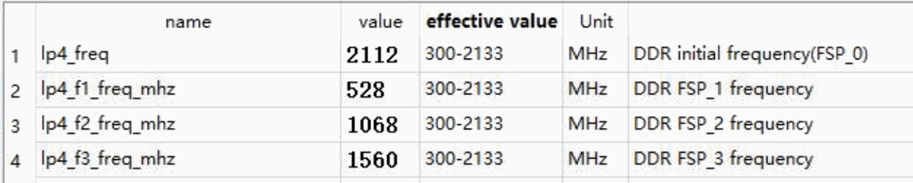
Editable screenshot transcription (original fields and values):
| Parameter | Value | Valid range | Unit | Description |
|---|---|---|---|---|
| lp4_freq | 2112 | 300-2133 | MHz | DDR initial frequency (FSP_0) |
| lp4_f1_freq_mhz | 528 | 300-2133 | MHz | DDR FSP_1 frequency for scaling |
| lp4_f2_freq_mhz | 1068 | 300-2133 | MHz | DDR FSP_2 frequency for scaling |
| lp4_f3_freq_mhz | 1560 | 300-2133 | MHz | DDR FSP_3 frequency for scaling |
Change serial port

Editable screenshot transcription (original fields and values):
| Parameter | Value | Valid range | Unit | Description |
|---|---|---|---|---|
| uart id | 0 | — | UART ID; 0xf disables UART output |
Change serial port baud rate

Editable screenshot transcription (original fields and values):
| Parameter | Value | Valid range | Unit | Description |
|---|---|---|---|---|
| uart id | 0 | — | UART ID; 0xf disables UART output | |
| uart iomux | 0 | — | UART IOMUX | |
| uart baudrate | 1500000 | bps | Supports 115200 or 1500000 |
1.6 How to Change DDR Frequency in U-Boot
RK322x
The following modification method is only supported by RK322x. The method is to modify arch/arm/boot/dts/rk322x.dtsi in kernel-3.10 code.
dram: dram {
    compatible = "rockchip,rk322x-dram";
    status = "okay";
    dram_freq = <786000000>;
    rockchip,dram_timing = <&dram_timing>;
};
You just need to modify “dram_freq” in the above code block and unit here is Hz. The frequency can be selected freely.
U-Boot will parse this DTS automatically, then read and scale it to the corresponding frequency.
RK3576/RK3588
The following modification method is only supported by RK3576 and RK3588. When the loader initializes DDR, these platforms will initialize 4 DDR frequencies together for subsequent kernel use, and will exit the loader at the highest frequency by default and continue with the following procedures.
The following F1, F2, F3, and F0 are these four frequencies. The default is to exit with F0.
DDR ... v1.14
LPDDR4X, 2112MHz
channel[0] BW=16 Col=10 Bk=8 CS0 Row=16/0 CS1 Row=16/0 CS=2 Die BW=16 Size=2048MB
channel[1] BW=16 Col=10 Bk=8 CS0 Row=16/0 CS1 Row=16/0 CS=2 Die BW=16 Size=2048MB
channel[2] BW=16 Col=10 Bk=8 CS0 Row=16/0 CS1 Row=16/0 CS=2 Die BW=16 Size=2048MB
channel[3] BW=16 Col=10 Bk=8 CS0 Row=16/0 CS1 Row=16/0 CS=2 Die BW=16 Size=2048MB
...
change to F1: 528MHz /* 4 DDR frequencies */
change to F2: 1068MHz
change to F3: 1560MHz
change to F0: 2112MHz
out
When you need to modify the DDR frequency under U-Boot, you only need to modify the frequency of exiting the loader.
Through the tool described in “Modify the DDR bin file”, find the boot_fsp parameter, and you can choose which frequency of F0/F1/F2/F3 is used as the frequency to exit the loader. In this way, the DDR frequency in U-Boot can be modified.

Editable screenshot transcription (original fields and values):
| Parameter | Value | Valid range | Unit | Description |
|---|---|---|---|---|
| boot_fsp | 0 | — | DDR frequency entering the system after initialization: 0=fsp0, 1=fsp1, 2=fsp2, 3=fsp3 |
1.7 How to Enable/Disable the DDR Frequency Scaling Function in the Kernel
Firstly, confirm that the chip do support DDR frequency scaling in the kernel. After that, you can enable or disable frequency scaling feature as follow method:
For kernel 4.4 and later versions, you need to find the final dmc node in dts. Change the status to “disabled” to disable the DDR scaling function in the kernel. Conversely, changing to “okay” will enable DDR frequency scaling.
Note 1: For RK3576 and RK3588, after enabling DDR scaling function through the dts dmc node, check whether the “center-supply” and “mem-supply”attribute under the dmc node is correctly configured based on the power connect used by the actual product hardware. The configuration values of these attributes represent the name of the regulator nodes that provide power to the DDR module on the
SOC-side as well as to the LOGIC.
The default for RK3576 is center-supply = <&vdd_ddr_s0> , mem-supply = <&vdd_logic_s0> .
The default for RK3588 is center-supply = <&vdd_ddr_s0> , mem-supply = <&vdd_log_s0> .
If the dmc node lacks this attribute, the dmc driver will fail to load. The kernel log is as follows.
rockchip-dmc dmc: Cannot get the regulator "center"
Note 2: For other platforms, after enabling DDR scaling function through the dts dmc node, check whether the “center-supply” attribute under the dmc node is correctly configured based on the power connect used by the actual product hardware. The configuration value of this attribute represent the name of the regulator node that provide power to the DDR module on the SOC-side.
The default for RK3399 is center-supply = <&vdd_center> ;
and the default for other platforms such as PX30/RK3568/RV1126 is center-supply=<&vdd_logic> .
If the dmc node lacks this attribute, the dmc driver will fail to load. The kernel log is as follows.
rockchip-dmc dmc: Cannot get the regulator "center"
Note 3: It is better keep dfi node status consistent with dmc node because dmc node restricted by dfi node in the lagacy code, dfi node “disabled “ would make the dmc node invalid.
For example, RK3399 EVB, the final dmc node is in arch/arm64/boot/dts/rockchip/rk3399-evb.dtsi .
&dfi {
    status = "okay";
};
&dmc {
    center-supply = <&vdd_center>; /* This requires the customer to configure it according
to the actual hardware circuit*/
    status = "okay"; /* enable kernel DDR scaling function */
    ...
};
&dfi {
    status = "disabled";
};
&dmc {
    status = "disabled"; /* disable kernel DDR scaling function */
    ...
};
For kernel 3.10, you need to find the final clk_ddr_dvfs_table node in dts. Modify the status to “disabled” to disable the DDR scaling function in the kernel. Conversely, modify to “okay “will enable the DDR scaling function.
For example, the final clk_ddr_dvfs_table of the RK3288 SDK board is in arch/arm/boot/dts/rk3288-tb_8846.dts.
&clk_ddr_dvfs_table {
    ...
    status="okay"; /* enable kernel DDR scaling function */
};
&clk_ddr_dvfs_table {
    ...
    status="disabled"; /* disable kernel DDR scaling function */
};
For kernel 3.0, you need to modify dvfs_ddr_table in the board-level borad-**.c file, leaving only one DDR_FREQ_NORMAL frequency in the table, so that DDR cannot change frequency.
For example, the board file of the RK3066 SDK board is in arch/arm/mach-rk30/board-rk30-sdk.c as below:
/* This table enable DDR scaling function */
static struct cpufreq_frequency_table dvfs_ddr_table[] = {
    {.frequency = 200 * 1000 + DDR_FREQ_SUSPEND, .index = 1050 * 1000},
    {.frequency = 300 * 1000 + DDR_FREQ_VIDEO, .index = 1050 * 1000},
    {.frequency = 400 * 1000 + DDR_FREQ_NORMAL, .index = 1125 * 1000},
    {.frequency = CPUFREQ_TABLE_END},
};
/* This table disable DDR scaling function */
static struct cpufreq_frequency_table dvfs_ddr_table[] = {
    //{.frequency = 200 * 1000 + DDR_FREQ_SUSPEND, .index = 1050 * 1000},
    //{.frequency = 300 * 1000 + DDR_FREQ_VIDEO, .index = 1050 * 1000},
    {.frequency = 400 * 1000 + DDR_FREQ_NORMAL, .index = 1125 * 1000},
    {.frequency = CPUFREQ_TABLE_END},
};
1.8 How to Prohibit DDR Scaling include in initialization state
The previous topic just talk about how to enable or disable DDR scaling function ,keeping you machine running without scaling.But there is a exception in initialization,DDR will scale frequency once in ddr_init when you power on, to update DDR timing for higher performance.So if you need disable DDR scaling function include in ddr_init , you need modify code referred to Chapter “How to Enable/Disable the DDR Frequency Scaling Function in the Kernel” and the code below:
For kernel 4.4 and later versions
Only following the Chapter “How to Enable/Disable the DDR Frequency Scaling Function in the Kernel”,DDR frequency scaling will stop working, included in ddr_init .
For kernel 3.10
Chip Type : RK322X
Code Location: NO code in kernel
Method: Modify dram node to “disabled” only
dram: dram {
    compatible = "rockchip,rk322x-dram";
    status = "disabled"; /* Please,modify here! */
    dram_freq = <786000000>;
    rockchip,dram_timing = <&dram_timing>;
};
Chip type : RK3188
Code Location: ddr_init() function in the file arch/arm/mach-rockchip/ddr_rk30.c
Chip type : RK3288
Code Location: ddr_init() function in the file arch/arm/mach-rockchip/ddr_rk32.c
Chip type : RK3126B, RK3126C which firmware without trust.img
Code Location: ddr_init() function in the file arch/arm/mach-rockchip/ddr_rk3126b.c
Chip type : RK3126/RK3128
Code Location: ddr_init() function in the file ./arch/arm/mach-rockchip/ddr_rk3126.c
Method: comment out the following lines in ddr_init() function code :
if(freq != 0)
    value = clk_set_rate(clk, 1000*1000*freq);
else
    value = clk_set_rate(clk, clk_get_rate(clk));
Chip type : RV1108
Code Location: ddr_init() function in the file arch/arm/mach-rockchip/ddr_rv1108.c
Method: comment out the following lines in ddr_init() function code :
if (freq == 0)
_ddr_change_freq(ddr_freq_current);
else
_ddr_change_freq(freq);
The other chip, included RK3126B and RK3126C which firmware with trust.img, only need to do following the Chapter “How to Enable/Disable the DDR Frequency Scaling Function in the Kernel”, DDR frequency scaling will stop working, included in ddr_init . For kernel 3.0
Code Path
| Chip Type | Code Path |
|---|---|
| RK3066 | arch/arm/mach-rk30/ddr.c, ddr_init() function |
| RK3026, RK3028A | arch/arm/mach-rk2928/ddr.c, ddr_init() function |
arch/arm/mach-rk2928/ddr.c, ddr_init() function
Method: comment out the following lines in ddr_init() function code
if(freq != 0)
    value=ddr_change_freq(freq);
else
    value=ddr_change_freq(clk_get_rate(clk_get(NULL, "ddr"))/1000000);
1.9 How to Check the DDR Capacity
If you look for a DDR capacity roughly, using the following command to check the MemTotal capacity. This capacity looks a little smaller than real, please estimate it to an integer value.
root@rk3399:/ # cat /proc/meminfo
MemTotal: 3969804 kB
If you need for more detail about DDR capacity, follow this:
DDR capacity printing in 2 places,which is in DDR initialization stage in loader and kernel. There is no printing of DDR capacity information in kernel 4.4 and later versions;Some chip have DDR capacity information in kernel 3.10(see the table below). The DDR capacity details in the loader are available on all chips. The DDR capacity printing in the loader must be captured by the serial port, if using ADB, you will miss this part.
| Chip Type | loader | kernel 3.0/3.10/ kernel 4.4 and later versions |
|---|---|---|
| RK3026 | √ | √ |
| RK3028A | √ | √ |
| RK3036 | √ | × |
| RK3066 | √ | √ |
| RK3126 | √ | √ |
| RK3126B, RK3126C with trust.img | √ | × |
| RK3126B, RK3126C without trust.img | √ | √ |
| RK3128 | √ | √ |
| RK3188 | √ | √ |
| RK322x | √ | × |
| RK322xh | √ | × |
| RK3288 | √ | √ |
| RK3328 | √ | × |
| RK3368 | √ | × |
| RK3399 | √ | × |
| RV1108 | √ | × |
| Other SOC | √ | × |
√ means have capacity printing
× means no capacity printing
The DDR detail contains: DDR type/DDR frequency/Channel (channel a/ channel b)/bus width(BW)/row/column(col)/bank(BK)/CS/die bus width(die BW)/size (total capability)
The whole capacity equals to “Size” or “Total capacity” when SOC chip only has 1 DDR channel or the sum of two channel’s “Size” or “Total capacity”.
The detail of DDR capacity in the loader as below:
DDR Version 1.05 20170712
In
Channel a: DDR3 400MHz
Bus Width=32 Col=10 Bank=8 Row=15 CS=1 Die Bus-Width=16 Size=1024MB
Channel b: DDR3 400MHz
Bus Width=32 Col=10 Bank=8 Row=15 CS=1 Die Bus-Width=16 Size=1024MB
Memory OK
Memory OK
OUT
The detail of DDR capacity in the kernel as below:
[ 0.528564] DDR DEBUG: version 1.00 20150126
[ 0.528690] DDR DEBUG: Channel a:
[ 0.528701] DDR DEBUG: DDR3 Device
[ 0.528716] DDR DEBUG: Bus Width=32 Col=10 Bank=8 Row=15 CS=1 Total Capability=1024MB
[ 0.528727] DDR DEBUG: Channel b:
[ 0.528736] DDR DEBUG: DDR3 Device
[ 0.528750] DDR DEBUG: Bus Width=32 Col=10 Bank=8 Row=15 CS=1 Total Capability=1024MB
[ 0.528762] DDR DEBUG: addr=0xd40000
1.10 Modify DDR capacity
At present, the DDR capacity of all Rockchip platforms is automatically recognized and does not require customers to configure DDR capacity. Methods for modifying DDR capacity are provided here, mainly for customers to evaluate performance or evaluate the impact of reducing DDR capacity.
In “Rockchip_Developer_Guide_UBoot_Nextdev_CN” -> “CH08 Debugging Methods” -> “Modify DDR Capacity”, another modification method is provided.
When booting, the DDR initialization code will pass the DDR capacity to U-Boot, and U-Boot will remove some secure memory and then pass it to the kernel. Users can modify the DDR capacity passed to the kernel during the U-Boot stage.
Code location:
./arch/arm/mach-rockchip/param.c
Modification steps:
1. Add print to view current DDR capacity information
struct memblock *param_parse_ddr_mem(int *out_count)
{
    ...
    for (i = 0, n = 0; i < count; i++, n++) {
        base = t->u.ddr_mem.bank[i];
        size = t->u.ddr_mem.bank[i + count];
        printf("base:0x%llx, size:0x%llx\n", base, size); //Add this line to print
        /* 0~4GB */
        if (base < SZ_4GB) {
            mem[n].base = base;
            mem[n].size = ddr_mem_get_usable_size(base, size);
    ...
}
After making the above modifications, recompile U-Boot and download it. In the new U-Boot startup log, there is the following output.
U-Boot 2017.09-g0236dc3682-220712-dirty #hcy (Aug 04 2022 - 10:46:07 +0800)
Model: Rockchip RK3568 Evaluation Board
PreSerial: 2, raw, 0xfe660000
DRAM: base:0x0, size:0x40000000 //This line is the output we added
in
base:0x0, size:0x40000000
As shown in the figure below, there is 1 DRAM space, the base address is 0x0, and the size is 0x40000000
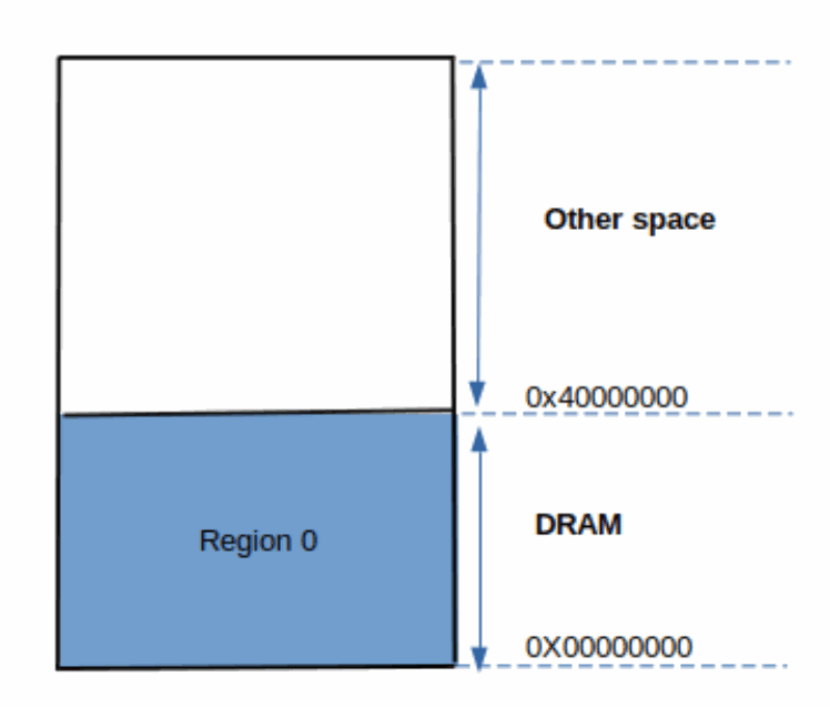
Before U-Boot boots the kernel, U-Boot removes some secure memory and passes the DDR capacity information to the kernel as follows.
Adding bank: 0x00200000 - 0x08400000 (size: 0x08200000) //After removing the secure memory
block
Adding bank: 0x09400000 - 0x40000000 (size: 0x36c00000) //After removing the secure memory
block
Total: 1182.666 ms
Starting kernel ...
[ 0.000000] Booting Linux on physical CPU 0x0000000000 [0x412fd050]
2. After understanding the description method of the above DDR capacity information, you can modify it.
Assume that a piece of DRAM space is added to the system, as shown in the location of Region 1 in the figure below. You can make the following modifications:
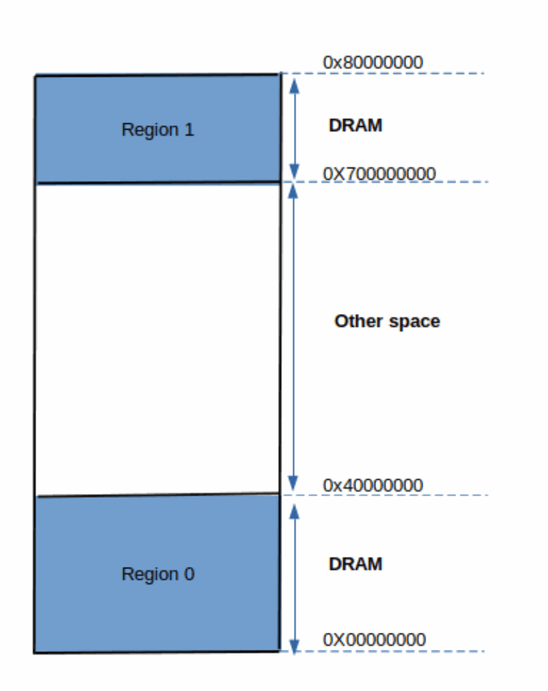
struct memblock *param_parse_ddr_mem(int *out_count)
{
    ...
    /* extend top ram size */
    if (t->u.ddr_mem.flags & DDR_MEM_FLG_EXT_TOP)
        gd->ram_top_ext_size = t->u.ddr_mem.data[0];
    //Modify DDR capacity information,starting here
    count = 2;
    t->u.ddr_mem.count = count;
    t->u.ddr_mem.bank[0] = 0x0; //Region 0 base address
    t->u.ddr_mem.bank[0 + count] = 0x40000000 - 0x0; //Region 0 size
    t->u.ddr_mem.bank[1] = 0x70000000; //Region 1 base address
    t->u.ddr_mem.bank[1 + count] = 0x80000000 - 0x70000000; //Region 1 size
    t->u.ddr_mem.hash = 0;
    ///Modify DDR capacity information, end here
    /* normal ram size */
    count = t->u.ddr_mem.count;
    mem = calloc(count + MEM_RESV_COUNT, sizeof(*mem));
    if (!mem) {
        printf("Calloc ddr memory failed\n");
        return 0;
    }
    ...
    for (i = 0, n = 0; i < count; i++, n++) {
        base = t->u.ddr_mem.bank[i];
        size = t->u.ddr_mem.bank[i + count];
        printf("base:0x%llx, size:0x%llx\n", base, size);
        /* 0~4GB */
        if (base < SZ_4GB) {
            mem[n].base = base;
            mem[n].size = ddr_mem_get_usable_size(base, size);
    ...
}
Let’s focus on analyzing the following code:
    count = 2; //Indicates that there are 2 blocks of DRAM space
    t->u.ddr_mem.count = count; //Must be written like this
    t->u.ddr_mem.bank[0] = 0x0;
    t->u.ddr_mem.bank[0 + count] = 0x40000000 - 0x0; //The array index must have "+count"
    //Region base address plus Region size is One group, how many groups there are, must be
the same as the "count" above
    t->u.ddr_mem.bank[1] = 0x70000000;
    t->u.ddr_mem.bank[1 + count] = 0x80000000 - 0x70000000; //The array index must have
"+count"
    t->u.ddr_mem.hash = 0; //Must be written like this
Recompile U-Boot and download it. In the new boot log, you can see that the modifications have taken effect.
...
U-Boot 2017.09-g0236dc3682-220712-dirty #hcy (Aug 04 2022 - 10:46:07 +0800)
Model: Rockchip RK3568 Evaluation Board
PreSerial: 2, raw, 0xfe660000
DRAM: base:0x0, size:0x40000000
base:0x70000000, size:0x10000000 //this is what we have added
...
Adding bank: 0x00200000 - 0x08400000 (size: 0x08200000)
Adding bank: 0x09400000 - 0x40000000 (size: 0x36c00000)
Adding bank: 0x70000000 - 0x80000000 (size: 0x10000000) //this is what we have added
Total: 1182.666 ms
Starting kernel ...
[ 0.000000] Booting Linux on physical CPU 0x0000000000 [0x412fd050]
If the customer still only has one DRAM, but wants to change the size to 0x80000000, he can add the following code.
count = 1; //Indicates that there is 1 block
t->u.ddr_mem.count = count; //Must be written like this
t->u.ddr_mem.bank[0] = 0x0;
t->u.ddr_mem.bank[0 + count] = 0x80000000 - 0x0; //The array index must have "+count"
t->u.ddr_mem.hash = 0; //Must be written like this
==Note: The DRAM capacity cannot be increased at will, because without real storage, the system will be abnormal. Generally, the size is changed to a smaller size for evaluation. Region1 is added to the example here for ease of understanding.==
1.11 Check DDR frequency
by devfreq
If the DDR frequency scaling function is enabled, the current DDR frequency can be obtained through the following nodes
cat /sys/class/devfreq/dmc/cur_freq
console:/ # cat /sys/class/devfreq/dmc/cur_freq
780000000
by clk_summary
cat /sys/kernel/debug/clk/clk_summary | grep scmi_clk_ddr
or
cat /sys/kernel/debug/clk/clk_summary | grep sclk_ddrc
or
cat /sys/kernel/debug/clk/clk_summary | grep sclk_ddr
Depends on the kernel version.
console:/ # cat /sys/kernel/debug/clk/clk_summary | grep scmi_clk_ddr
scmi_clk_ddr 0 0 0 2736000000 0 0 50000
/*2736000000 is the DDR frequency in Hz, that is, 2736MHz*/
1.12 How to Modify DDR Frequency
There are 2 strategies in the kernel: scenario frequency scaling and loading frequency scaling. The operation between kernel 4.4 (and later versions) and kernel 3.10 has some difference.
kernel 4.4 and later versions:
Scenario frequency scaling means: entered the specified scenario, DDR frequency will change to the corresponding frequency defined by SYS_STATUS_XXX if the load frequency scaling function disabled.In the contrary, load frequency scaling function is enable, it will increase or reduce frequency based on the actual DDR status and the defined value of upthreshold/downdifferential , but frequency will not be lower than the value from SYS_STATUS_XXX .
Load frequency scaling means: The frequency depends on the load status in all scenario, but higher than the defined value from SYS_STATUS_XXX .Only the special SYS_STATUS_NORMAL is replaced by load frequency value, and the lowest frequency was controlled by auto-min-freq instead of SYS_STATUS_NORMAL .
kernel 3.10:
Scenario frequency scaling means: Entered the specific scenario, DDR frequency change to the value of SYS_STATUS_XXX and no more change though the load frequency scaling function is enabled.
Load frequency scaling means: it is used to replace scenario SYS_STATUS_NORMAL , DDR frequency depends on the load status only in SYS_STATUS_NORMAL .
To modify the DDR frequency, it still has to be handled by kernel branch separately.
PX30S/RK3326S, see “PX30S/RK3326S DDR frequency selection” on the back
The platforms listed in Chapter “Platform with 4 frequency points DDR bin”, see “Platform with 4 frequency points DDR bin, its DDR frequency selection” on the back
For kernel 4.4, it requires get the dmc node in dts. For example, dmc node in RK3399 EVB is in arch/arm64/boot/dts/rockchip/rk3399-evb.dtsi and arch/arm64/boot/dts/rockchip/rk3399.dtsi
&dmc {
    status = "okay";
    center-supply = <&vdd_center>;
    upthreshold = <40>;
    downdifferential = <20>;
    system-status-freq = <
        /*system status freq(KHz)*/
        SYS_STATUS_NORMAL 800000
        SYS_STATUS_REBOOT 528000
        SYS_STATUS_SUSPEND 200000
        SYS_STATUS_VIDEO_1080P 200000
        SYS_STATUS_VIDEO_4K 600000
        SYS_STATUS_VIDEO_4K_10B 800000
        SYS_STATUS_PERFORMANCE 800000
        SYS_STATUS_BOOST 400000
        SYS_STATUS_DUALVIEW 600000
        SYS_STATUS_ISP 600000
    >;
    /* Each line is used as a group of data, "min_bw "and "max_bw" represent the bandwidth
requirement corresponded by vop.When the requirement value fallling between the range of
"min_bw" and "max_bw", the DDR frequency needs to increase the frequency specified by
"freq", and is valid at "auto-freq-en=1" */
    vop-bw-dmc-freq = <
    /* min_bw(MB/s) max_bw(MB/s) freq(KHz) */
        0 577 200000
        578 1701 300000
        1702 99999 400000
    >;
    auto-min-freq = <200000>;
};
dmc: dmc {
    compatible = "rockchip,rk3399-dmc";
    devfreq-events = <&dfi>;
    interrupts = <GIC_SPI 1 IRQ_TYPE_LEVEL_HIGH 0>;
    clocks = <&cru SCLK_DDRCLK>;
    clock-names = "dmc_clk";
    ddr_timing = <&ddr_timing>;
    /* DDR utilization exceeds 40%, starts to increase frequency when "auto-freq-en=1 " */
    upthreshold = <40>;
    /* DDR utilization less than 20%, start to reduce frequency when "auto-freq-en=1 " */
    downdifferential = <20>;
    system-status-freq = <
    /*system status freq(KHz)*/
    /* It is valid when "auto-freq-en=0". It indicates that this scene is in common use
except for the following scenes */
    SYS_STATUS_NORMAL 800000
    /* It means the DDR frequency before reboot. When auto-freq-en=1, this frequency will be
used as the min value and increased according to the load status */
    SYS_STATUS_REBOOT 528000
    /* It means the DDR frequency at early suspend. When auto-freq-en=1, this frequency will
be used as the min value and increased according to the load status */
    SYS_STATUS_SUSPEND 200000
    /* It means the DDR frequency at playing 1080P video.When auto-freq-en=1, this frequency
will be used as the min value and increased according to the load status */
    SYS_STATUS_VIDEO_1080P 300000
    /* It means the DDR frequency at playing 4K video When auto-freq-en=1, this frequency
will be used as the min value and increased according to the load status */
    SYS_STATUS_VIDEO_4K 600000
    /* It means the DDR frequency at playing 4K 10bit video. When auto-freq-en=1, this
frequency will be used as the min value and increased according to the load status */
    SYS_STATUS_VIDEO_4K_10B 800000
    /* It means the DDR frequency at performance mode.When auto-freq-en=1, this frequency
will be used as the min value and increased according to the load status */
    SYS_STATUS_PERFORMANCE 800000
    /* It means the DDR frequency at touching,getting higher frequency from low in order to
improve touching respond.When auto-freq-en=1, this frequency will be used as the min value
and increased according to the load status */
    SYS_STATUS_BOOST 400000
    /* It means the DDR frequency at dual display mode.When auto-freq-en=1, this frequency
will be used as the min value and increased according to the load status */
    SYS_STATUS_DUALVIEW 600000
    /* It means the DDR frequency at ISP mode.When auto-freq-en=1, this frequency will be
used as the min value and increased according to the load status */
    SYS_STATUS_ISP 600000
    >;
    /* When auto-freq-en=1, this frequency will be used as the min value of
SYS_STATUS_NORMAL scenario */
    auto-min-freq = <400000>;
    /* The value equals to 1,which indicates this function is on, to 0,which means off.If it
is on, "SYS_STATUS_NORMAL" will be taken by the load frequency completely and the lowest
frequency is" auto-min-freq" instead of "SYS_STATUS_NORMAL".That means,it takes the
frequency defined by this scene as the lowest frequency and the system will increase or
reduece DDR frequency through "upthreshold/downdifferential" according to DDR utilization */
    auto-freq-en = <1>;
    status = "disabled";
};
==Note 1==: Kernel 4.4 frequency voltage is different from kernel 3.10, it runs in this frequency only when frequency equals to opp-hz listed by dmc_opp_table .If the frequency less than opp-hz , compatible to it upwardly,otherwise, it exceeds opp-hz the upper limited,it will restricted by opp-hz .So, if you do not want to be controlled, you should concern dmc_opp_table .
dmc_opp_table: opp-table3 {
    opp-200000000 {
        /* When the DDR frequency equals to 200MHz,this voltage is effective;less than
200MHz,running at 200MHz */
        opp-hz = /bits/ 64 <200000000>;
        opp-microvolt = <825000>; //vdd_center voltage
    };
    ...
    opp-800000000 {
        opp-hz = /bits/ 64 <800000000>;
        opp-microvolt = <900000>;
    };
};
After understanding the meaning of each configuration, modify the corresponding frequency definition according to the scene you need to modify. If auto-freq-en=1 , it is not good to control the frequency. If reducing frequency is to locate problem, you can set auto-freq-en value to 0, then modify the frequency value defined by each scene to achieve your purpose.
==Note 2==: For RK3399 LPDDR4 and RV1126 platforms, the frequency supported by DDR frequency scaling has been determined in the loader stage, and these frequencies will be printed out through the serial port during the DDR initialization stage, and the kernel frequencies defined by dmc_opp_table needs to correspond to it.
Taking RV1126 as an example, the DDR frequencies printed in the loader stage are 328MHz, 528MHz, 784MHz, and 924MHz, so dmc_opp_table can only define these four frequencies.
change to: 328MHz
change to: 528MHz
change to: 784MHz
change to: 924MHz(final freq)
dmc_opp_table: dmc-opp-table {
    compatible = "operating-points-v2";
    opp-328000000 {
        opp-hz = /bits/ 64 <328000000>;
        opp-microvolt = <800000>;
    };
    opp-528000000 {
        opp-hz = /bits/ 64 <528000000>;
        opp-microvolt = <800000>;
    };
    opp-784000000 {
        opp-hz = /bits/ 64 <784000000>;
        opp-microvolt = <800000>;
    };
    opp-924000000 {
        opp-hz = /bits/ 64 <924000000>;
        opp-microvolt = <800000>;
    };
};
If the frequencies define by dmc_opp_table and the loader are inconsistent, a frequency mismatch problem will occur when the kernel dmc driver performs DDR frequency scaling. The log is as follows.
rockchip-dmc dmc: Get wrong frequency, Request 1056000000, Current 924000000
To kernel3.10, it requires to find the node clk_ddr_dvfs_table in dts. For example, RK3288 SDK’s last node clk_ddr_dvfs_table is in arch/arm/boot/dts/rk3288-tb_8846.dts .
&clk_ddr_dvfs_table {
    /* The logic voltage corresponding to the DDR frequency, if the frequency in "freq-
table" or "bd-freq-table" is larger than the maximum frequency here, the corresponding
voltage cannot be found and can not switched to the corresponding frequency. At this time,
you need to add frequency voltage table here */
    operating-points = <
        /* KHz uV */
        200000 1050000
        300000 1050000
        400000 1100000
        533000 1150000
        >;
    freq-table = <
        /*status freq(KHz)*/
        /* It is valid only when "auto-freq-en=0".And it indicates that this scene is common
use scene except for the following scenes */
        SYS_STATUS_NORMAL 400000
        /* DDR frequency at the early suspend */
        SYS_STATUS_SUSPEND 200000
        /* DDR frequency at playing 1080P video */
        SYS_STATUS_VIDEO_1080P 240000
        /* DDR frequency at playing 4K video */
        SYS_STATUS_VIDEO_4K 400000
        /* DDR frequency at playing 60FPS video */
        SYS_STATUS_VIDEO_4K_60FPS 400000
        /* DDR frequency at performance mode */
        SYS_STATUS_PERFORMANCE 528000
        /* DDR frequency at dual display */
        SYS_STATUS_DUALVIEW 400000
        /* DDR frequency at touching,getting higher frequency from low in order to improve
touching respond */
        SYS_STATUS_BOOST 324000
        /* DDR frequency at ISP */
        SYS_STATUS_ISP 400000
        >;
    bd-freq-table = <
        /* bandwidth freq */
        5000 800000
        3500 456000
        2600 396000
        2000 324000
    >;
    /* After the load frequency scaling turned on,where the "SYS_STATUS_NORMAL" scenario, it
will switch between several frequencies listed by this table according to the DDR bandwidth
utilization */
    auto-freq-table = <
        240000
        324000
        396000
        528000
        >;
    /* The value equals to "1", indicating that the load frequency conversion function is
enabled; equals to 0, means disabled. After the load frequency conversion function turning
on, the "SYS_STATUS_NORMAL" scene frequency scaling will be completely replaced by the load
scaling frequency */
    auto-freq=<1>;
    /*
     * 0: use standard flow
     * 1: vop dclk never divided
     * 2: vop dclk always divided
     */
    vop-dclk-mode = <0>;
    status="okay";
};
After understanding the meaning of each configuration, modify the corresponding frequency definition according to the scene you need to modify. If auto-freq-en=1 , it is not good to control the frequency. If reducing frequency is to locate problem, you can set auto-freq-en value to 0, then modify the frequency value defined by each scene to achieve your purpose.
==Note: you must make sure that the voltage can work at this frequency==.As for how to modify voltage, see the chapter “How to modify the voltage corresponding to a certain DDR frequency “.
To kernel3.10, it requires to find the dvfs_ddr_table in board document borad-**.c . For example, RK3066 SDK’s dvfs_ddr_table is in arch/arm/mach-rk30/board-rk30-sdk.c .
static struct cpufreq_frequency_table dvfs_ddr_table[] = {
    /* DDR frequency at the early suspend */
    {.frequency = 200 * 1000 + DDR_FREQ_SUSPEND, .index = 1050 * 1000},
    /* DDR frequency at playing video */
    {.frequency = 300 * 1000 + DDR_FREQ_VIDEO, .index = 1050 * 1000},
    /* it indicates that this scene is common use scene except for above two scenes */
    {.frequency = 400 * 1000 + DDR_FREQ_NORMAL, .index = 1125 * 1000},
    {.frequency = CPUFREQ_TABLE_END},
};
Kernel 3.0 has only 3 scenes. The DDR frequency to be modified is in “200 * 1000” of .frequency and the frequency unit here is KHz. The “+ DDR_FREQ_SUSPEND” string can be ignored.
==Note: you must make sure that the voltage can work at this frequency==.As for how to modify voltage, see the chapter “How to modify the voltage corresponding to a certain DDR frequency “.
1.12.1 RK3399 LPDDR4 supports 928MHz modification method
1. Modify the RKBOOT/RK3399MINIALL.ini file in the rkbin directory, select the 933MHz DDR bin file, and pack the loader.
diff --git a/RKBOOT/RK3399MINIALL.ini b/RKBOOT/RK3399MINIALL.ini
index d8e71dd7..3e20f255 100755
--- a/RKBOOT/RK3399MINIALL.ini
+++ b/RKBOOT/RK3399MINIALL.ini
@@ -5,7 +5,7 @@ MAJOR=1
 MINOR=26
 [CODE471_OPTION]
 NUM=1
-Path1=bin/rk33/rk3399_ddr_800MHz_v1.27.bin
+Path1=bin/rk33/rk3399_ddr_933MHz_v1.27.bin
 Sleep=1
 [CODE472_OPTION]
 NUM=1
@@ -14,7 +14,7 @@ Path1=bin/rk33/rk3399_usbplug_v1.26.bin
 NUM=2
 LOADER1=FlashData
 LOADER2=FlashBoot
-FlashData=bin/rk33/rk3399_ddr_800MHz_v1.27.bin
+FlashData=bin/rk33/rk3399_ddr_933MHz_v1.27.bin
 FlashBoot=bin/rk33/rk3399_miniloader_v1.26.bin
 [OUTPUT]
 PATH=rk3399_loader_v1.27.126.bin
After download the pack loader file into the machine, you can see from the log printed by the serial port that the loader supports five frequency scaling: 416MHz, 856MHz, 328MHz, 666MHz, and 928MHz. The current running DDR frequency is 856MHz.
DDR Version 1.27 20211018
In
...
support 416 856 328 666 928 MHz, current 856MHz
OUT
2. Modify the kernel dts dmc_opp_table node and change the status = “disabled” in the opp- 928000000 table to status =”okay” , or delete it directly.
                opp-928000000 {
                        opp-hz = /bits/ 64 <928000000>;
                        opp-microvolt = <900000>;
- status = "disabled";
                };
3. Modify the kernel dts dmc node and change all “856000” in the system-status-freq table to “928000”, or refer to this document The “How to Modify DDR Frequency” chapter describes the SYS_STATUS_XXX related Scenario frequency scaling, which can be selectively modified according to the DDR bandwidth requirements of different scenarios in the actual project.
1.12.2 PX30S/RK3326S DDR frequency selection
For the RK3326S/PX30S platform, only 4 frequency points are supported. They are configed by ddrx_params node in arch/arm64/boot/dts/rockchip/px30s-dram-default-timing.dtsi and px30s_dmc_opp_table node in arch/arm64/boot/dts/rockchip/px30.dtsi .
For the ddrx_params node, if DDR3 for example, should config the freq_0, freq_1, freq_2, freq_3 in ddr3_params. If DDR4, should config the freq_0, freq_1, freq_2, freq_3 in ddr4_params.
For the px30s_dmc_opp_table node, all types of DDR are share a single frequency table. The enabling frequency must correspond to the freq_0, freq_1, freq_2, freq_3 in ddrx_params. For example, if LPDDR4, the enabled frequency of px30s_dmc_opp_table must correspond to freq_0, freq_1, freq_2, freq_3 in lpddr4_params. The configuration is as follows:
px30s_dmc_opp_table: px30s-dmc-opp-table {
    compatible = "operating-points-v2";
    opp-328000000 {
        opp-hz = /bits/ 64 <328000000>;
        opp-microvolt = <1000000>;
    };
    opp-666000000 {
        opp-hz = /bits/ 64 <666000000>;
        opp-microvolt = <1000000>;
    };
    opp-786000000 {
        opp-hz = /bits/ 64 <786000000>;
        opp-microvolt = <1000000>;
    };
    opp-924000000 {
        opp-hz = /bits/ 64 <924000000>;
        opp-microvolt = <1000000>;
    };
    /* 1056M only for LP4 */
    opp-1056000000 {
        opp-hz = /bits/ 64 <1056000000>;
        opp-microvolt = <1000000>;
        status = "disabled";
    };
};
/ {
    ...
    lpddr4_params: lpddr4-params {
        ...
        /* freq info, freq_0 is final frequency, unit: MHz */
        freq_0 = <924>;
        freq_1 = <328>;
        freq_2 = <666>;
        freq_3 = <786>;
        ...
    };
};
If the LPDDR4 needs to run 1056 MHz, you need to change one of the frequency values of freq_0, freq_1, freq_2, freq_3 in lpddr4_params to 1056. In addition, the px30s_dmc_opp_table node should disable old frequency points and add 1056000000 frequency points.
The new configuration is as follows:
px30s_dmc_opp_table: px30s-dmc-opp-table {
    compatible = "operating-points-v2";
    opp-328000000 {
        opp-hz = /bits/ 64 <328000000>;
        opp-microvolt = <1000000>;
    };
    opp-666000000 {
        opp-hz = /bits/ 64 <666000000>;
        opp-microvolt = <1000000>;
    };
    opp-786000000 {
        opp-hz = /bits/ 64 <786000000>;
        opp-microvolt = <1000000>;
    };
    opp-924000000 {
        opp-hz = /bits/ 64 <924000000>;
        opp-microvolt = <1000000>;
        status = "disabled";
    };
    /* 1056M only for LP4 */
    opp-1056000000 {
        opp-hz = /bits/ 64 <1056000000>;
        opp-microvolt = <1000000>;
    };
};
/ {
    ...
    lpddr4_params: lpddr4-params {
        ...
        /* freq info, freq_0 is final frequency, unit: MHz */
        freq_0 = <1056>;
        freq_1 = <328>;
        freq_2 = <666>;
        freq_3 = <786>;
        ...
    };
};
1.12.3 Platform with 4 frequency points DDR bin, its DDR frequency selection
The platforms listed in Chapter “Platform with 4 frequency points DDR bin”, excluding RV1126, all other platforms are compatible with the methods describe in this section.
These platforms’ loader changes the frequency 4 times and saves the training results of the corresponding frequencies.
The following F1, F2, F3, and F0 are these four frequencies. The default is to exit with F0.
DDR ... v1.14
LPDDR4X, 2112MHz
channel[0] BW=16 Col=10 Bk=8 CS0 Row=16/0 CS1 Row=16/0 CS=2 Die BW=16 Size=2048MB
channel[1] BW=16 Col=10 Bk=8 CS0 Row=16/0 CS1 Row=16/0 CS=2 Die BW=16 Size=2048MB
channel[2] BW=16 Col=10 Bk=8 CS0 Row=16/0 CS1 Row=16/0 CS=2 Die BW=16 Size=2048MB
channel[3] BW=16 Col=10 Bk=8 CS0 Row=16/0 CS1 Row=16/0 CS=2 Die BW=16 Size=2048MB
...
change to F1: 528MHz /* 4 DDR frequencies*/
change to F2: 1068MHz
change to F3: 1560MHz
change to F0: 2112MHz
out
For these platforms, although the frequency supported by DDR frequency scaling is also determined in the loader stage, the kernel dmc driver will automatically obtain the supported DDR frequency value, so there is no dmc_opp_table frequency matching problem. The kernel dmc nodes for these platforms are as follows
dmc: dmc {
    ...
    system-status-freq = <
    /*system status freq(KHz)*/
    SYS_STATUS_NORMAL DMC_FREQ_LEVEL_MID_HIGH
    SYS_STATUS_REBOOT DMC_FREQ_LEVEL_MID_LOW
    ...
    SYS_STATUS_SUSPEND DMC_FREQ_LEVEL_LOW
    ...
    SYS_STATUS_PERFORMANCE DMC_FREQ_LEVEL_HIGH
    ...
    >;
    ...
};
The frequencies corresponding to each scene are no longer direct frequencies, but definitions such as DMC_FREQ_LEVEL_HIGH. These definitions can automatically match to the 4 frequencies of the loader. If you use the “Modify the DDR bin file” method to modify 4 frequencies, DMC_FREQ_LEVEL_HIGH and other definitions can automatically change to the modified 4 frequencies. Taking the above four frequencies of the boot loader as an example, the corresponding relationship is as follows:
| Macro definition | frequency | illustrate |
|---|---|---|
| DMC_FREQ_LEVEL_HIGH | F0 2112MHz | Highest frequency |
| DMC_FREQ_LEVEL_MID_HIGH | F3 1560MHz | sub-high frequency |
| DMC_FREQ_LEVEL_MID_LOW | F2 1068MHz | sub-low frequency |
| DMC_FREQ_LEVEL_LOW | F1 528MHz | lowest frequency |
To modify the frequency values corresponding to F0, F1, F2, and F3, please refer to “Modify the DDR bin file”.
To modify the frequency corresponding to the scenario, such as SYS_STATUS_NORMAL or SYS_STATUS_REBOOT, replace the corresponding frequency with one of DMC_FREQ_LEVEL_HIGH, DMC_FREQ_LEVEL_MID_HIGH, DMC_FREQ_LEVEL_MID_LOW, or DMC_FREQ_LEVEL_LOW.
1.13 How to Modify the Voltage Corresponding to A Certain DDR Frequency
If you want to locate bug through changing the voltage by command, use the following method: Versions after kernel 4.4: You can directly adjust the voltage of a certain regulator through the /sys/kernel/debug/regulator/ node. DDR frequency must be fixed first, otherwise, the regulate voltage here will conflict with the regulate voltage of DDR frequency scaling. DDR fixed frequency reference chapter “How to fix DDR frequency”.
Take 3588 regulate voltage as an example:
cat /sys/kernel/debug/regulator/vdd_ddr_s0/voltage
echo 700000 > /sys/kernel/debug/regulator/vdd_ddr_s0/voltage
The regulators that need to be adjusted to modify the voltage corresponding to the DDR frequency on each platform are as follows:
| Platform | Nodes that need to be adjusted |
|---|---|
| RK3308/RK3308B | “vdd_core” or “vdd_log” |
| RK3576 | “vdd_logic_s0” and “vdd_ddr_s0” |
| RK3588 | “vdd_log_s0” and “vdd_ddr_s0” |
| Other SOC | “vdd_center” or “vdd_logic” |
kernel 4.4: You need to compile the kernel, select “pm_tests” option (make ARCH=arm64 menuconfig - >Device Drivers -> SOC (System On Chip) specific Drivers -> Rockchip pm_test support )
kernel 3.10: You need to compile the kernel, open “pm_tests” option (make menuconfig ->System Type -> /sys/pm_tests/ support ).
The command to modify the DDR voltage is:
RK3399
echo set vdd_center 900000 > /sys/pm_tests/clk_volt
Other Chip
echo set vdd_logic 1200000 > /sys/pm_tests/clk_volt
If there is no “pm_tests” or the command cannot meet the requirements, you need to change the kernel firmware, as follows:
For kernel 4.4, you need to find the node dmc_opp_table in dts. For example,RK3399 EVB’s node is in arch/arm64/boot/dts/rockchip/rk3399-opp.dtsi ,RK3368’s node is in arch/arm64/boot/dts/rockchip/rk3368.dtsi
Take RK3399 as an example:
/* it runs in this frequency only when frequency equals to "opp-hz"listed by
"dmc_opp_table".If the frequency less than "opp-hz", the frequency will getting
higher,otherwise, it exceeds "opp-hz" the upper limited,it will restricted by "opp-hz".It is
different from kernel 3.10 */
dmc_opp_table: opp-table3 {
    compatible = "operating-points-v2";
    opp-200000000 {
        /* When the DDR frequency equals to 200MHz,this voltage is effective;less than
200MHz,running at 200MHz */
        opp-hz = /bits/ 64 <200000000>;
        opp-microvolt = <825000>; //vdd_center voltage
    };
    opp-300000000 {
        opp-hz = /bits/ 64 <300000000>;
        opp-microvolt = <850000>;
    };
    opp-400000000 {
        opp-hz = /bits/ 64 <400000000>;
        opp-microvolt = <850000>;
    };
    opp-528000000 {
        opp-hz = /bits/ 64 <528000000>;
        opp-microvolt = <900000>;
    };
    opp-600000000 {
        opp-hz = /bits/ 64 <600000000>;
        opp-microvolt = <900000>;
    };
    opp-800000000 {
        opp-hz = /bits/ 64 <800000000>;
        opp-microvolt = <900000>;
    };
};
Take RK3368 as an example:
/* it runs in this frequency only when frequency equals to "opp-hz"listed by
"dmc_opp_table".If the frequency less than "opp-hz", the frequency will getting
higher,otherwise, it exceeds "opp-hz" the upper limited,it will restricted by "opp-hz".It is
different from kernel 3.10 */
dmc_opp_table: opp_table2 {
    compatible = "operating-points-v2";
    opp-192000000 {
        /* When the DDR frequency equals to 200MHz,this voltage is effective;less than
200MHz,running at 200MHz */
        opp-hz = /bits/ 64 <192000000>;
        opp-microvolt = <1100000>; //vdd_logic voltage
    };
    opp-300000000 {
        opp-hz = /bits/ 64 <300000000>;
        opp-microvolt = <1100000>;
    };
    opp-396000000 {
        opp-hz = /bits/ 64 <396000000>;
        opp-microvolt = <1100000>;
    };
    opp-528000000 {
        opp-hz = /bits/ 64 <528000000>;
        opp-microvolt = <1100000>;
    };
    opp-600000000 {
        opp-hz = /bits/ 64 <600000000>;
        opp-microvolt = <1100000>;
    };
};
The voltage in accordance with the frequency can be modified. Since the frequency-voltage table using voltage less than or equal to the specified frequency, the added frequency that exceeds the limited frequency of this table cannot match the appropriated voltage, which will cause DDR fail to switch to the new frequency. At this time, it is necessary to add a frequency-voltage item corresponding to the frequency.
For kernel 3.10, you need to find the node clk_ddr_dvfs_table in dts , for example, RK3288 SDK the last clk_ddr_dvfs_table is in arch/arm/boot/dts/rk3288-tb_8846.dts .
&clk_ddr_dvfs_table {
    /* This is Frequency-voltage table */
    operating-points = <
        /* KHz uV */
        /* it is show when DDR frequency less than or equals to 200MHz,logic voltage uses
1050mV.Other lines mean the same here */
        200000 1050000
        300000 1050000
        400000 1100000
        533000 1150000
        >;
    ...
    status="okay";
};
The voltage in accordance with the frequency can be modified. Since the frequency-voltage table using voltage less than or equal to the specified frequency, the added frequency that exceeds the limited frequency of this table cannot match the appropriated voltage, which will cause DDR fail to switch to the new frequency. At this time, it is necessary to add a frequency-voltage item corresponding to the frequency.
For kernel 3.0, you need to modify dvfs_ddr_table in the file borad-**.c ,for example, RK3066 SDK’s
borad-**.c is in arch/arm/mach-rk30/board-rk30-sdk.c .
static struct cpufreq_frequency_table dvfs_ddr_table[] = {
    {.frequency = 200 * 1000 + DDR_FREQ_SUSPEND, .index = 1050 * 1000},
    {.frequency = 300 * 1000 + DDR_FREQ_VIDEO, .index = 1050 * 1000},
    {.frequency = 400 * 1000 + DDR_FREQ_NORMAL, .index = 1125 * 1000},
    {.frequency = CPUFREQ_TABLE_END},
};
The “.index” in the dvfs_ddr_table is the corresponding voltage,unit here is uV.
1.14 How to Disable the Load DDR Frequency Scaling with Leaving Only the Scene Frequency Scaling
For kernel 4.4 and later versions, you need to find auto-freq-en of the dmc node in dts.For example, RK3399 EVB’s auto-freq-en is in arch/arm64/boot/dts/rockchip/rk3399.dtsi .
dmc: dmc {
    compatible = "rockchip,rk3399-dmc";
    ...
    auto-min-freq = <400000>;
    /* Set this value to 0 to close the load DDR Frequency scaling with leaving only the
scene frequency scaling */
    auto-freq-en = <0>;
    ...
};
For kernel 3.10, you need to find the node clk_ddr_dvfs_table in dts, For example, RK3288 EVB’s clk_ddr_dvfs_table is in arch/arm/boot/dts/rk3288-tb_8846.dts
&clk_ddr_dvfs_table {
    ...
    /* Set this value to 0 to close the load DDR Frequency scaling with leaving only the
scene frequency scaling */
    auto-freq=<0>;
    ...
    status="okay";
};
Kernel 3.0 itself does not support the load frequency scaling, let alone closing it.
1.15 How to Fix DDR Frequency
If you want to locate bug through fixing DDR frequency by command, use the following method:
kernel 4.4 and later versions:
Get the available DDR frequency: cat /sys/class/devfreq/dmc/available_frequencies
Set frequency:
echo userspace > /sys/class/devfreq/dmc/governor
echo 300000000 > /sys/class/devfreq/dmc/min_freq //This line purposes to prevent the frequency to be set lower than "min_freq", cause operation failed.
echo 300000000 > /sys/class/devfreq/dmc/userspace/set_freq
kernel 3.10:
You need to compile the kernel, open “pm_tests” option (make menuconfig ->System Type -> /sys/pm_tests/ support ) , Fixing DDR frequency command is
echo set clk_ddr 300000000 > /sys/pm_tests/clk_rate
The frequency unit here is Hz and the command parameter can be changed according to the requirement.
If the method above is not feasible, you can only modify the code or dts.
For kernel 4.4 and later versions, if the method above does not work, it is generally because the target frequency, not in cat /sys/class/devfreq/dmc/available_frequencies .
The way to solve this problem is to find the board-level dts file and add your target frequency in dmc_opp_table . For example, the RK3399 EVB board is in arch/arm64/boot/dts/rockchip/rk3399- opp.dtsi .Here assuming you want to add 666MHz:
dmc_opp_table: opp-table3 {
compatible = "operating-points-v2";
opp-200000000 {
    opp-hz = /bits/ 64 <200000000>;
    opp-microvolt = <825000>;
};
...
opp-666000000 {
    /* When DDR frequency equals to 666MHz,use this voltage */
    opp-hz = /bits/ 64 <666000000>;
    opp-microvolt = <900000>; //vdd_center voltage
};
opp-800000000 {
    opp-hz = /bits/ 64 <800000000>;
    opp-microvolt = <900000>;
};
};
After that, you can just use the previous command to fix the frequency.
If you do not want to fix frequency through inputing command at power-on, but starts from at a fixed frequency, modify the dts as beblow:
Supposed your target frequency is 666MHz. For example, the dmc node of RK3399 EVB board is in arch/arm64/boot/dts/rockchip/rk3399-evb.dtsi
/* Here "dfi" status must be "okay", it is due to lagacy code, the dmc node is
restriced by the dfi node. If the "dfi" node is disabled, it will also invalidate the
dmc node. So it is best to keep the status of the "dfi" node consistent with dmc */
&dfi {
    status = "okay";
};
&dmc {
status = "okay";
...
system-status-freq = <
    /*system status freq(KHz)*/
    SYS_STATUS_NORMAL 666000
    /* Remove the rest scenario */
    /*
    SYS_STATUS_REBOOT 528000
    SYS_STATUS_SUSPEND 200000
    SYS_STATUS_VIDEO_1080P 200000
    SYS_STATUS_VIDEO_4K 600000
    SYS_STATUS_VIDEO_4K_10B 800000
    SYS_STATUS_PERFORMANCE 800000
    SYS_STATUS_BOOST 400000
    SYS_STATUS_DUALVIEW 600000
    SYS_STATUS_ISP 600000
    */
>;
...
auto-min-freq = <666000>;
/* The value of "auto-freq-en" shall be 0 to disable load DDR Frequency scaling */
auto-freq-en = <0>;
};
For kernel 3.10, you need to find the node clk_ddr_dvfs_table , for example, RK3288 SDK’s clk_ddr_dvfs_table is in arch/arm/boot/dts/rk3288-tb_8846.dts .
&clk_ddr_dvfs_table {
    operating-points = <
        /* KHz uV */
        /* step 3,if the target frequency exceeds the maximun of this table,you shall add
the voltage table corresponding to the target frequency */
        200000 1050000
        300000 1050000
        400000 1100000
        533000 1150000
        >;
    freq-table = <
        /*status freq(KHz)*/
        /* step 2, Comment out the other scenario,keep "SYS_STATUS_NORMAL" and define it to
you target frequency, for example you need 400MHz as below */
        SYS_STATUS_NORMAL 400000
        /*
        SYS_STATUS_SUSPEND 200000
        SYS_STATUS_VIDEO_1080P 240000
        SYS_STATUS_VIDEO_4K 400000
        SYS_STATUS_VIDEO_4K_60FPS 400000
        SYS_STATUS_PERFORMANCE 528000
        SYS_STATUS_DUALVIEW 400000
        SYS_STATUS_BOOST 324000
        SYS_STATUS_ISP 400000
        */
        >;
    bd-freq-table = <
        /* bandwidth freq */
        5000 800000
        3500 456000
        2600 396000
        2000 324000
    >;
    auto-freq-table = <
        240000
        324000
        396000
        528000
        >;
    /* setp 1,set 0 to disable load DDR Frequency scaling */
    auto-freq=<0>;
    /*
     * 0: use standard flow
     * 1: vop dclk never divided
     * 2: vop dclk always divided
     */
    vop-dclk-mode = <0>;
    status="okay";
};
Just 3 steps can finish fixing frequency firmware.
1. The load frequency part should be set to 0
2. Comment out the other scenario,keep “SYS_STATUS_NORMAL” and define it to your target frequency
3. If the target frequency exceeds the maximun of this table,you shall add the voltage table corresponding to the target frequency.
For kernel 3.0,you need to modify dvfs_ddr_table in borad-**.c . For example ,RK3066 SDK’s borad- **.c is in arch/arm/mach-rk30/board-rk30-sdk.c
static struct cpufreq_frequency_table dvfs_ddr_table[] = {
    /* */
    /* step 1. Comment out the other scene with leaving "DDR_FREQ_NORMAL" only */
    //{.frequency = 200 * 1000 + DDR_FREQ_SUSPEND, .index = 1050 * 1000},
    //{.frequency = 300 * 1000 + DDR_FREQ_VIDEO, .index = 1050 * 1000},
    /* step 2, Define "DDR_FREQ_NORMAL" to your target frequency,meanwhile pay attention to
whether the voltage match the frequency or not */
    {.frequency = 400 * 1000 + DDR_FREQ_NORMAL, .index = 1125 * 1000},
    {.frequency = CPUFREQ_TABLE_END},
};
Just 2 steps can finish fixing frequency firmware.
1. Comment out the other scene with leaving “DDR_FREQ_NORMAL” only
2. Define “DDR_FREQ_NORMAL” to your target frequency,meanwhile pay attention to whether the voltage match the frequency or not
1.16 How to get the DDR Bandwidth Utilization
Kernel 4.4 and later versions provides a command that can show the whole DDR bandwidth utilization,
rk3288:/sys/class/devfreq/dmc # cat load
11@396000000Hz
“11” Indicates that the current bandwidth utilization of DDR is 11%.
Rockchip also provides an executable file dedicated to observing DDR bandwidth. Please refer to the “Rockchip DDR Bandwidth Tool Instructions” chapter for details.
1.17 How to Test the Reliability of DDR
Please see the document “DDR-Verification-Process”
1.18 How to Check the Maximum Working Frequency of DDR
1. Add the frequency-voltage table to the corresponding frequency first, if you don’t know how to ,please see the chapter “How to Modify DDR Frequency” and “How to Modify the Voltage Corresponding to A Certain DDR Frequency”.
2. See the “Rockchip DDR DQ Eye Tool Guide” chapter to confirm the eye diagram for platforms that provide eye diagram tools.
3. Run google stressapptest from high frequency to low frequency, when you get an error, lower the frequency and run it again. No error, you can run it for more time. If it still works well, go to the next step.
google stressapptest in https://redmine.rock-chips.com/documents/49 -> DDR related information_VerX.XX.7z -> DDR particle verification_DDR test resource file-> static_stressapptest For details on how to use it, see the “Guide_DDR_Verification_Process” chapter.
4. The previous step has roughly figured out the highest frequency. Now run a memtester. The same, when you get an error, lower the frequency and run it again. No error, you can run for a while, If it still works well, you can confirm the highest frequency point.
memtester is at https://redmine.rock-chips.com/documents/49 -> DDR related information_VerX.XX.7z -> DDR particle verification_DDR test resource file-> static_memtester For details on how to use it, please refer to the “Guide_DDR_Verification_Process” chapter.
“Google stressapptest” is a rough process,which can quickly report error. And “ memtester” is more careful, so it reports error more slow. But “memtester” is mainly for the signal test, can cover the part that “google stressapptest” missing.
Apparently, the methods above are all based on the software test, which used to quickly get the maximum frequency. It is not sure the actual DDR SI can meet the JEDEC standard at the maximum frequency,that is necessary to measure the signal and burn-test.
1.19 How to Judge DDR in Self-Refresh Mode
It can be judged by measuring the CKE signals and it does not need an oscilloscope with a very high bandwidth.
| CKE State | Explanation |
|---|---|
| Low level (Time>7.8us) | in self-refresh state |
| High level | in normal state |
If the measured CKE is low period and high period, it is also can be regard as to the table above, that is, it enters the self-refresh mode and exit to normal state after a while.
Note: The time when CKE is low must be more than 7.8 us before self-refresh entry because power-down state also has a low CKE, but the time is less than 7.8 us. Please do not confuse it.
1.20 How to Judge DDR in Auto power-down Mode
It can be judged by measuring the CKE signals and it does not need an oscilloscope with a very high bandwidth.
| CKE State | Explanation |
|---|---|
| Low level (Time<7.8us) | in power-down state |
| High level | in normal state |
In the auto power-down mode, the measured CKE state holds low for nearly 7.8us (DDR3/DDR4) or 3.9us (LPDDR2/LPDDR3/ LPDDR4) and high for a short period of time, then enters low level for 7.8us or 3.9us for loop.
Note: The time when CKE is low must be less than 7.8 us(DDR3/DDR4), 3.9us(LPDDR2/LPDDR3/LPDDR4), which can be judged a auto power-down.
1.21 Disable self-refresh and power-down modes
All DDR chips have basic power-saving functions such as self-refresh and power-down. These functions are also enabled in the software to save power. When the DDR is idle, it will enter the self-refresh or power-down mode according to the idle time.
Some customers do not need the power-saving function; or only care about performance but not power consumption; or there are problems with the self-refresh or power-down functions of the DDR chips. You can disable these power-saving modes by the following method.
Set the value of sr_idle in the figure below to 0 to disable the function of allowing the DDR chips to enter self- refresh according to the DDR idle time.

Editable screenshot transcription (original fields and values):
| Parameter | Value | Valid range | Unit | Description |
|---|---|---|---|---|
| uart id | 2 | — | UART ID; 0xf disables UART output | |
| uart iomux | 0 | — | UART IOMUX | |
| uart baudrate | 1500000 | bps | Supports 115200 or 1500000 | |
| sr_idle | 93 | 0-1023 | 32clk | Idle DRAM clock cycles before self refresh; 0 disables |
| pd_idle | 13 | 0-127 | 32clk | Idle DRAM clock cycles before power down; 0 disables |
Set the value of pd_idle in the figure below to 0 to disable the function of allowing the DDR chips to enter
power-down according to the DDR idle time.
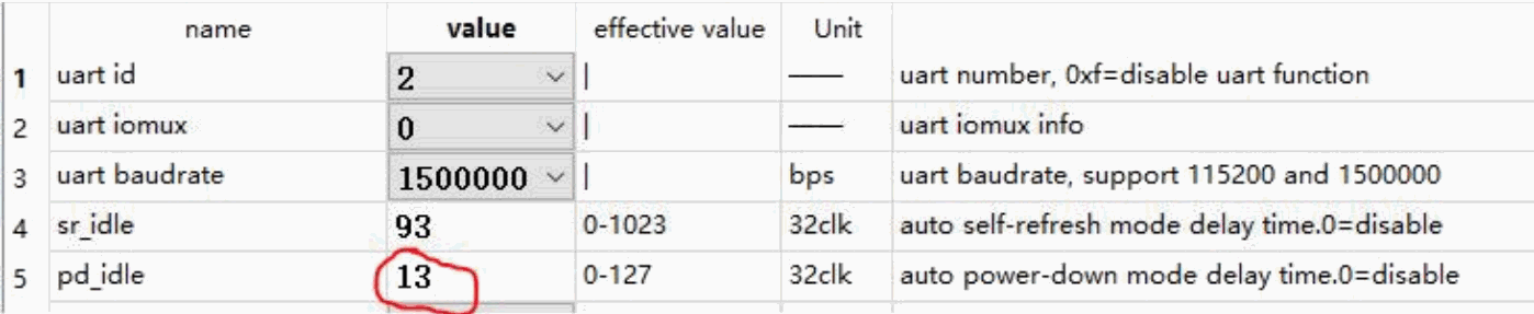
Editable screenshot transcription (original fields and values):
| Parameter | Value | Valid range | Unit | Description |
|---|---|---|---|---|
| uart id | 2 | — | UART ID; 0xf disables UART output | |
| uart iomux | 0 | — | UART IOMUX | |
| uart baudrate | 1500000 | bps | Supports 115200 or 1500000 | |
| sr_idle | 93 | 0-1023 | 32clk | Idle DRAM clock cycles before self refresh; 0 disables |
| pd_idle | 13 | 0-127 | 32clk | Idle DRAM clock cycles before power down; 0 disables |
1.22 How to Adjust the De-skew of DQ/DQS/CA/CLK
Mainly due to the unequal length of DDR routing in hardware PCB, the skew can be adjusted to achieve the effect similar to the same length of DDR routing. The skew function is the delay units in series on the signal line inside the DDR PHY. The delay of each signal line can be changed by controlling the number of delay units in series on each signal line through the skew register.
1.22.1 Adjusting the de-skew in kernel
Only RK322Xh/RK3328 support modifying the de-skew in kernel. The method is modify dts.
Chip Type: RK322xh, RK3328
Code location:
arch/arm64/boot/dts/rk322xh-dram-default-timing.dtsi
arch/arm64/boot/dts/rk322xh-dram-2layer-timing.dtsi
If customer have new file replace above file, please modify your new file.
Modify method:
According to the results of the released tool “deskew automatic scanning tool”, select the “mid” value and add it to the corresponding dts definition.
Please according to “3228H deskew automatic scanning tool instruction. pdf” to use “deskew automatic scanning tool”.
1.22.2 Adjusting the de-skew in loader
Only RK3308 support modifying the de-skew in loader.
Chip Type: RK3308
Required documents:
deskew automatic scanning tool, 3308_deskew.exe, RK3308_DDRXPXXXXXX_Template_VXX_de-skew.txt, rk3308_ddr_XXXMHz_uartX_mX_vX.XX.bin
Modify method:
According to the results of the released tool “deskew automatic scanning tool”, select the “mid” value and add it to the corresponding definition in RK3308_DDRXPXXXXXX_Template_VXX_de-skew.txt. Using 3308_deskew.exe, change the definition of de-skew on rk3308_ddrxpxxxxxx_template_vxx_de-skew.txt to rk3308_ddr_xxxmhz_uartx_mx_vx.xx.bin.
Please according to “deskew automatic scanning tool instruction. pdf” to use “deskew automatic scanning tool”.
1.23 Run DDR stress test under U-Boot
Under U-Boot, we have porting two commonly used DDR stress test programs, stressapptest and memtester.
Mainly used for:
When the kernel fails to start, perform a stress test on the DDR under U-Boot to eliminate DDR problems.
The kernel does not have the conditions to run stressapptest or memtester.
For example, if there are many incomplete modules in the kernel, it will cause system instability and make stressapptest or memtester unable to run for a long time.
Test larger DDR space
The kernel can only test the remaining DDR space due to system usage. Testing under U-Boot occupies much less space and can test a larger DDR space.
Specify physical address test
1.23.1 stressapptest
enable
make ARCH=arm64 menuconfig ->Command line interface -> DDR Tool -> Enable DDR Tool
and enable
make ARCH=arm64 menuconfig ->Command line interface -> DDR Tool -> Enable DDR Tool -> Enable stressapptest for ddr
Compile U-Boot and download uboot.img.
Restart the device. On the PC serial terminal, keep pressing the CTRL+C keys until U-Boot enters the command line mode, as follows
  pclk_top_root 100000 KHz
  aclk_low_top_root 396000 KHz
Net: No ethernet found.
Hit key to stop autoboot('CTRL+C'): 0
=> <INTERRUPT>
=> <INTERRUPT>
Enter stressapptest -h , and follow the parameter instructions to test.
1.23.2 memtester
enable
make ARCH=arm64 menuconfig ->Command line interface -> DDR Tool -> Enable DDR Tool
and enable
make ARCH=arm64 menuconfig ->Command line interface -> DDR Tool -> Enable DDR Tool -> Enable memtester for ddr
Compile U-Boot and download uboot.img.
Restart the device. On the PC serial terminal, keep pressing the CTRL+C keys until U-Boot enters the command line mode, as follows
  pclk_top_root 100000 KHz
  aclk_low_top_root 396000 KHz
Net: No ethernet found.
Hit key to stop autoboot('CTRL+C'): 0
=> <INTERRUPT>
=> <INTERRUPT>
Enter memtester -h , and follow the parameter instructions to test.
1.24 Enable RK3568 ECC
ECC refers to Error Correcting Code, and DDR ECC performs error checking and correction on DDR data.
RK3568 supports SideBand ECC, which adds a DDR die next to the DDR data channel dedicated to storing ECC data.
Its ECC has the ability to correct 1 bit and detect 2 bit errors, namely SEC/DED ECC (Single Error Correction/Double Error Detection).
1. Enable ECC: As long as DDR_ECC_DQ0-7 has DDR chip attached, ECC will be automatically enabled.
2. The function of DDR_ECC_DQ0-7: The implementation of ECC is 32-bit DQ data + 7-bit ECC data.
DDR_ECC_DQ0-7 is used to store the ECC data calculated from DQ0-DQ31. Therefore, an additional DDR chip needs to be attached in DDR_ECC_DQ0-7 to store ECC data.
3. Requirements for the additional DDR chip: the DRAM type; number of rows, columns, banks; all must be the same as the DDR chip on DQ0-31.
4. Supported DRAM types: All DRAM types support ECC.
1.25 How to obtain DDR ECC information in the kernel
DDR ECC information is in the edac architecture of the kernel. For platforms that support DDR ECC function, such as RK3568, and the hardware have DDR ECC enabled(see the “Enable RK3568 ECC” chapter for details). To obtain DDR ECC information, first enable the edac module in dtsi. If the platform dtsi does not have an edac node, it means that the platform does not support it.
edac: edac {
    ...
    status = "okay";
};
RK EDAC will be registered to the system at the following location:
sys/devices/system/edac/mc/mc0
or
sys/bus/edac/devices/mc/mc0/
Get RK EDAC name:
# cat sys/devices/system/edac/mc/mc0/mc_name
rk_edac_ecc
Get the number of single-bit correctable errors (ce) accumulated after this startup:
# cat sys/devices/system/edac/mc/mc0/ce_count
0
Get the number of multi-bit uncorrectable errors (ue) accumulated after this startup:
# cat sys/devices/system/edac/mc/mc0/ue_count
0
When the system restarts, the kernel will reinitialize the related EDAC modules and counters, that is, the number of previously recorded errors will be cleared and counting will start from zero.
1.26 How to Inject DDR ECC Errors in the Kernel
To inject DDR ECC errors in the kernel, you need to ensure that the corresponding platform Device Tree Source (DTS) file in the kernel has the “edac” node enabled and that the hardware supports DDR ECC.
edac: edac {
        ...
        status = "okay";
    };
After the system boots up, you can choose the type of DDR ECC error to inject using the following node:
echo ce > /sys/module/rockchip_edac/parameters/edac_poison_mode
echo ue > /sys/module/rockchip_edac/parameters/edac_poison_mode
The edac_poison_mode parameter supports the following two values:
1. ce: Injects single-bit correctable errors.
2. ue: Injects multi-bit uncorrectable errors.
To trigger the DDR ECC error, use the following node (the number you echo into it determines the quantity of DDR ECC errors to trigger):
echo 10 > /sys/module/rockchip_edac/parameters/rockchip_edac_trigger
Note:
1. If you encounter the following error message, make sure that EDAC is enabled in the kernel and that the hardware supports DDR ECC:
echo 1 > /sys/module/rockchip_edac/parameters/rockchip_edac_trigger
sh: echo: write error: Operation not permitted
2. The default behavior for multi-bit uncorrectable errors (ue) is to restart the system. For single-bit correctable errors (ce), the kernel’s default response is to log a warning and record the number of errors in the file /sys/devices/system/edac/mc/mc0/ce_count .
To inject DDR ECC errors in the HAL, please refer to the section “Rockchip_Developer_Guide_HAL_DDR_ECC” in the documentation.
1.27 How to get the DDR manufacturer ID
Only the LPDDR types (such as LPDDR2, LPDDR3, LPDDR4, LPDDR4X, LPDDR5, LPDDR5X) have manufacturer IDs, while the DDR types (such as DDR2, DDR3, DDR4) do not have manufacturer IDs.
1.27.1 dmcdbg node through kernel
The following platforms support obtaining DDR manufacturer ID through proc/dmcdbg/dmcinfo
RK3566
RK3568
RK3326
RK3326S
You need to first enable the dmcdbg node on the corresponding platform dtsi (if the node does not exist, this platform does not support it). For example, RK356X, in the arch/arm64/boot/dts/rockchip/rk3568.dtsi file, enable the dmcdbg node:
dmcdbg: dmcdbg {
    compatible = "rockchip,rk3568-dmcdbg";
    status = "okay";
};
After recompiling, update the kernel firmware, and booting it. You can get the DDR manufacturer ID and other DDR information through the command, cat proc/dmcdbg/dmcinfo .
console:/ # cat proc/dmcdbg/dmcinfo
DramType: LPDDR4
Dram ID: MR5=0x1,MR6=0x0,MR7=0x1 /* The MR5 is the manufacturer ID, and MR6 and MR7
are the version IDs reserved for the manufacturer definition */
DramCapacity:
CS Count: 1
Bus Width: 32 bit
Column: 10
Bank: 8
CS0_Row: 16
CS1_Row: 0
DieBusWidth: 16 bit
TotalSize: 2048 MB
devfreq/dmc: Enable
governor: dmc_ondemand
cur_freq: 780000000
NOTE:
more information about dmc can get from /sys/class/devfreq/dmc.
1.27.2 Output information through loader
RK3576/RK3588 loader output contains manufacturer ID
DDR ... v1.14
LPDDR5, 2736MHz
channel[0] BW=16 Col=10 Bk=16 CS0 Row=15 CS1 Row=15 CS=2 Die BW=16 Size=2048MB
channel[1] BW=16 Col=10 Bk=16 CS0 Row=15 CS1 Row=15 CS=2 Die BW=16 Size=2048MB
channel[2] BW=16 Col=10 Bk=16 CS0 Row=15 CS1 Row=15 CS=2 Die BW=16 Size=2048MB
channel[3] BW=16 Col=10 Bk=16 CS0 Row=15 CS1 Row=15 CS=2 Die BW=16 Size=2048MB
Manufacturer ID:0xff /* This is the manufacturer ID */
...
change to F0: 2736MHz
out
RK3399 loader output contains manufacturer ID
DDR Version ...
In
channel 0
...
MR5=0xFF /* This is the manufacturer ID */
...
change freq to 416MHz 0,1
Channel 0: LPDDR4,416MHz
Bus Width=32 Col=10 Bank=8 Row=16 CS=1 Die Bus-Width=16 Size=2048MB
Channel 1: LPDDR4,416MHz
Bus Width=32 Col=10 Bank=8 Row=16 CS=1 Die Bus-Width=16 Size=2048MB
...
OUT
1.27.3 Points to Note
The following points should be noted:
1. Only LPDDR types (such as LPDDR2, LPDDR3, LPDDR4, LPDDR4X, LPDDR5, LPDDR5X) have manufacturer ID, DDR type (such as DDR2, DDR3, DDR4) does not have a manufacturer ID.
2. The manufacturer ID shows the manufacturer of the wafer, not the packaged DDR brand information. Because many DDR vendors do not have the ability to produce wafers.
3. For all LPDDR, the model number on the packaging screen print cannot be obtained. This is different from Nand Flash or eMMC.
4. The resolution of the wafer manufacturer ID follows JEP166 of JEDEC standard.
1.27.4 Manufacturer ID table
The following is the latest Manufacturer ID table as of the completion of this document.
There will be updates in the future. You can search JEP166 at https://www.jedec.org to find the latest Manufacturer ID table.
LPDDR2, LPDDR3 Manufacturer ID table:
| MR5 value | Manufacturer name |
|---|---|
| 0x1 | Samsung |
| 0x2 | Qimonda |
| 0x3 | Elpida |
| 0x4 | Etron |
| 0x5 | Nanya |
| 0x6 | SK hynix |
| 0x7 | Mosel |
| 0x8 | Winbond |
| 0x9 | ESMT |
| 0xa | Zentel |
| 0xb | Spansion |
| 0xc | SST |
| 0xd | ZMOS |
| 0xe | Intel |
| 0x12 | Being Advanced Memory Corp |
| 0x1a | Xi’an UniIC Semiconductors Co., Ltd |
| 0x1b | ISSI |
| 0x1c | JSC |
| 0xaa | Tezzaron |
| 0xc2 | Macronix |
| 0xf8 | Fidelix |
| 0xfc | eveRAM |
| 0xfd | AP Memory |
| 0xfe | Numonyx |
| 0xff | Micron |
LPDDR4 Manufacturer ID table:
| MR5 value | Manufacturer name |
|---|---|
| 0x1 | Samsung |
| 0x5 | Nanya |
| 0x6 | SK hynix |
| 0x8 | Winbond |
| 0x9 | ESMT |
| 0x13 | CXMT |
| 0x1a | Xi’an UniIC Semiconductors Co., Ltd |
| 0x1c | JSC |
| 0xf8 | Fidelix |
| 0xf9 | Ultra Memory |
| 0xfd | AP Memory |
| 0xff | Micron |
LPDDR5 Manufacturer ID table:
| MR5 value | Manufacturer name |
|---|---|
| 0x1 | Samsung |
| 0x5 | Nanya |
| 0x6 | SK hynix |
| 0x8 | Winbond |
| 0x9 | ESMT |
| 0x13 | CXMT |
| 0xe5 | Dosilicon |
| 0xff | Micron |
1.28 Signal Related FAQs
1.28.1 tINIT3 does not satisfy the protocol
Reason: When the Rockchip platform performs DDR initialization, the RESET signal will reset multiple times. and the measurement manufacturer mistakenly used the high level of the first RESET signal as the measurement point of tINIT3, so the measured tINIT3 does not meet the protocol.
For the correct measurement method, the last RESET signal high level should be used as the measurement point of tINIT3. As shown below,
M2 cannot be used as the measurement point, but M3 should be used as the measurement point.
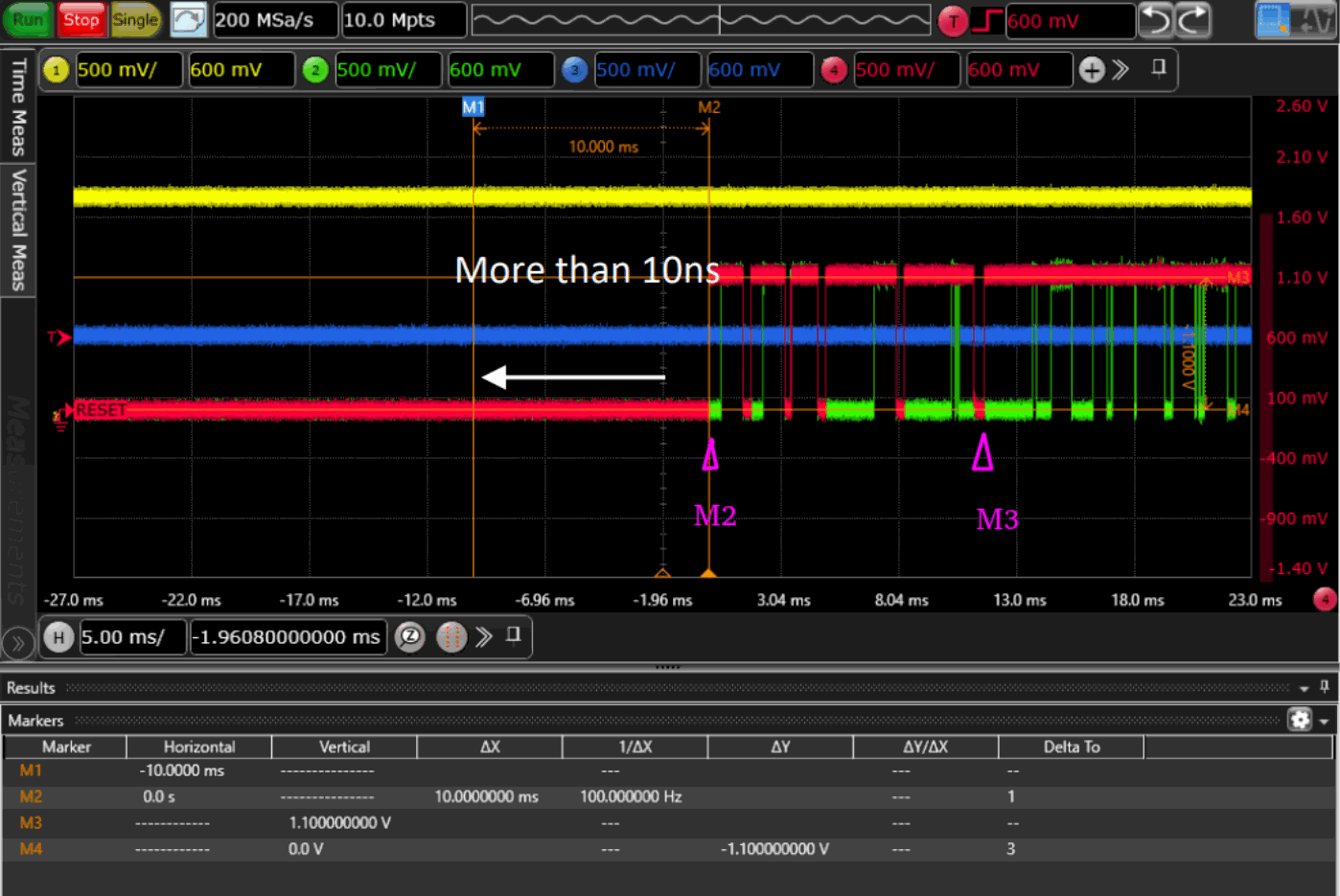
1.28.2 Note of enable DDR ODT
According to JEDEC standards, LPDDR4/LPDDR4X do not support enable ODT below 800MHz.
According to JEDEC standards, DDR4 do not support enable ODT below 625MHz.
1.29 High temperature refresh rate problem
When the temperature is higher than 85°C, the DDR needs to be refreshed twice rate.
This requirement requires special attention for industrial and automotive standard products.
Rockchip platform has the following methods to double refresh rate:
LPDDR4, LPDDR4X, LPDDR5, and LPDDR5X have their own temperature sensors, which can tell the required refresh rate through MR4 based on the temperature. Some Rockchip platforms implement a set of Automatic Temperature Derating functions, referred to as derate. The refresh rate can be automatically adjusted based on the MR4 information provided by the DDR die. This enables refresh rate and temperature matching.
LPDDR3 does not support the derate function due to some hardware reasons and forced double refreshed rate.
For DDR3 and DDR4, since they do not have a temperature sensor and do not have the function of MR4 to tell the required refresh rate, derate cannot be used. This type of DDR die requires forced double refreshed rate.
Customers can modify the ext_temp_ref of the DDR bin to double refresh rate

Editable screenshot transcription (original fields and values):
| Parameter | Value | Valid range | Unit | Description |
|---|---|---|---|---|
| ext_temp_ref | 0 | — | 0: Code decision (1x for normal chip, 2x for 3568M/3568J); 1: fix 2x refresh; 2: fix 4x refresh; 3: fix 1x refresh |
For modification method, see the “Modify the DDR bin file” chapter for details
Note: Rockchip’s industrial chips, automotive chips, and wide-temperature chips all have refresh rates modified, and there is no need to double them by yourself through this tool.
In the tool, the corresponding relationship between fixed 2x/4x/1x refresh is as follows
| ext_temp_ref | DDR2/DDR3/DDR4 | LPDDR3/LPDDR4/LPDDR4x/LPDDR5 |
|---|---|---|
| Fixed 1x refresh | tREFI=7.8us | tREFI=3.9us |
| Fixed 2x refresh | tREFI=3.9us | tREFI=1.95us |
| Fixed 4x refresh | tREFI=1.95us | tREFI=0.975us |
For conventional platforms that are not industrial chips, automotive chips, and wide-temperature chips, a refresh rate of 1x is used by default, except for DRAM with the derate function enabled.
The current Rockchip’s industrial chips, automotive chips, and wide-temperature chips processing methods and DDR bin version requirements are as follows:
| Platform | DDR type | Processing methods and DDR bin version requirements |
|---|---|---|
| RK3308J/M RK3308K RK3308GK |
All DDR types | Use rk3308_ddr_XXXMHz_uartX_mX_v1.26.bin and later versions default is 4x refresh (i.e. 0.25x tREFI) |
| RK3568J/M | LPDDR3 DDR3 DDR4 |
Use rk3568_ddr_XXXXMHz_v1.16.bin and later versions default is 2x refresh (i.e. 0.5x tREFI) |
| RK3568J/M | LPDDR4 LPDDR4X |
Use rk3568_ddr_XXXXMHz_v1.18.bin and later versions Enable the derate function by default |
| RK3588J/M | LPDDR4 LPDDR4X LPDDR5 LPDDR5X |
Use rk3588_ddr_XXXXMHz_v1.13.bin and later versions Enable the derate function by default |
| RV1126K | All DDR types | Use rv1126_ddr_XXXXMHz_v1.03.bin and later versions default is 2x refresh (i.e. 0.5x tREFI) |
The platforms with default DDR bin has the derate function enabled, as follows
| Platform | DDR type | Processing methods and DDR bin version requirements |
|---|---|---|
| RK3528 | LPDDR4 LPDDR4X |
Use rk3528_ddr_XXXXMHz_v1.07.bin or rk3528_ddr_XXXXMHz_2L_PCB_v1.07.bin or rk3528_ddr_XXXXMHz_4BIT_PCB_v1.07.bin` and later versions Enable the derate function by default |
| RK3562 | LPDDR4 LPDDR4X |
Use rk3562_ddr_XXXXMHz_v1.05.bin orrk3562_ddr_XXXXMHz_ultra_v1.05.bin and later versions Enable the derate function by default |
| RK3568 | LPDDR4 LPDDR4X |
Use rk3568_ddr_XXXXMHz_v1.18.bin and later versions Enable the derate function by default |
| RK3576 | LPDDR4 LPDDR4X LPDDR5 LPDDR5X |
Use rk3576_ddr_XXXXMHz_v1.00.bin and later versions Enable the derate function by default |
| RK3588 | LPDDR4 LPDDR4X LPDDR5 LPDDR5X |
Use rk3588_ddr_XXXXMHz_v1.13.bin and later versions Enable the derate function by default |
2. Chapter-2 DDR Troubleshooting Guide
2.1 How to confirm whether it is a DDR problem
1. View the UART log
1. If the UART log reports an error in the DDR initialization part of the loader , it must be a DDR problem.
2. Check whether the DDR capacity row, column, bank, DRAM type and bus width information in the DDR initialization part log in the loader is correct. If the information is wrong it may cause DDR problems.
3. If the UART log is a panic in the system, you can try several times to see if the panic addresses are consistent. If they are consistent, it is basically not a DDR problem. If they are inconsistent, it may be a DDR problem or a power integrity problem.
2. Check if the display is normal. If the display is abnormal, it is likely to be a DDR problem.
3. Perform a screening test:
1. Reduce the frequency of the ARM GPU and increase the voltage appropriately at the fixed frequency. If it works, it is not a DDR problem. It can basically be confirmed that it is a power supply problem.
2. Turn off the DDR Frequency Scaling function. If it works, the problem is likely to be caused by DDR frequency scaling.
3. Reduce the DDR frequency to a safe frequency (such as 324M). If it works, there is a high probability that there is a problem with the DDR signal quality.
2.2 Several main causes of DDR problems
1. Power supply problem:
1. The capacitors on the layout are not enough, the capacitors are placed too far from the chip, and the capacitor distribution is unreasonable.
2. The power feedback loop is not led back to the PMU/DC-DC end from the end as required.
3. Check whether the copper is processed according to the RK layout rules.
4. The GND directly below the LQFP packaged chip needs to be tinned to ensure good grounding, otherwise it will affect the internal power quality of the chip and heat dissipation.
2. Signal integrity issues:
1. Unequal length traces on the PCB. Some RK platforms do not have various read/write trainings, and unequal length traces will directly sacrifice the DDR setup/hold time.
2. Too narrow line spacing. Too narrow line spacing will cause serious crosstalk problems.
3. The branches of the T-type topology are of unequal length. The unequal length branches will
deteriorate the signal edge and make the edge non-monotonic.
4. Incompleteness of the signal reference layer loop. When copper is applied, the gap is set too large, resulting in the via directly cutting off the reference layer, which will cause the signal integrity issues.
3. DRAM component defect:
1. Some White Brand,since they have not been tested and some may even be eliminated by the factory, the yield cannot be guaranteed.
2. Some White Brand may have weak driver impedance.
3. Hynix 4Gb C die DDR3, such as H5TQ4G63CFR , kernel 3.10 early code needs to be patched before it can be used.
2.3 Some methods to solve DDR problems
The general way to solve DDR problems is to find pattern, and try to find the pattern of freezing, such as freezing at a certain frequency, whether the freezing after waking up from sleep is related to the sleep time, etc. Try various methods such as fixed frequency, trying different frequencies, raising voltage, changing drive strength, etc. to check the possibilities one by one and narrow down the scope of the problem.
1. Error log during DDR initialization
1. “rd addr 0x… = 0x…”, “16bit error!!!”,”unknow device”, it is basically a soldering problem. Soldering problems can be checked with the “Rockchip Platform DDR Test Tool” to directly find the problem.
2. For some DRAM capacity is not a power of 2, such as 768MB,1.5GB,3GB and other special DRAM, some versions of the code may not be compatible. You can update to the latest loader. If there are still abnormalities, you can contact DDR related engineers for analysis.
3. For the error reported in DDR loader , most of them are soldering problems. You can try to use the soldering special option of DDR test tool select the test items of corresponding capacity for test analysis.
2. Check whether the DDR capacity row, column , bank, bit width and DRAM type information in the DDR initialization part log of the loader is correct.
As shown in the figure below, the first line is the DDR code version, the third line is the DDR frequency, the fourth line is the DDR type, and the fifth line from left to right are the DRAM bus width, column number, bank number, row number, chip select number, die bus width and total capacity. Once the seventh line “OUT” showed, indicating that DDR initialization is successful and exits, and the following is the log printed by usbplug or miniloader. If the Die Bus-Width is larger than the actual one, there will be no problem, but if it is smaller than the actual one, it will cause a crash.

Editable screenshot transcription (original fields and values):
DDR Version V1.06 20171026
In
300MHz
DDR3
Bus Width=32 Col=10 Bank=8 Row=15 CS=2 Die Bus-Width=16 Size=2048MB
mach:14
OUT
Boot1 Release Time: 2017-06-12, version: 2.37
3. Check whether the display is normal.
When the system crashes, although the CPU stops, the vop will still repeatedly fetch data from the DDR
and display it on the screen. Therefore, when the system crashes, you can directly observe the display to preliminarily determine the status of the DDR at this time.
1. If the display is normal, it means that the DDR can be accessed normally, but it does not mean the exception is not caused by DDR.
2. If the display is abnormal.
As shown in the figure below,It may be that the DDR frequency switch process crashes and causes DDR to be inaccessible. At this time, you can try to fix the frequency. Or it may be a power supply problem that causes DDR controller logic abnormality.
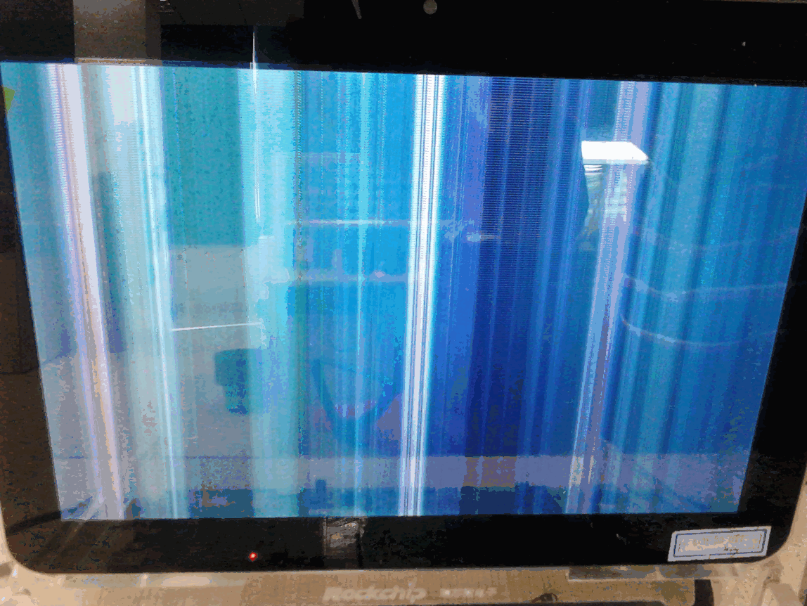
As shown in the figure below. PCB layout defects cause power integrity and signal integrity issues that cause DDR3 DLL to unlock. You can try to consider increasing VCC_DDR to 1.6V or dll bypass to solve the problem.

4. Check if it is a power supply problem
1. Fix the CPU/GPU to a lower frequency, and increase the arm/logic voltage. If there is any improvement, it may be Power problem.
2. Review the layout to see if there are any problems with the power supply.
3. Measure the power supply ripple.
5. Check if there is a signal integrity problem
1. Lower the DDR frequency. If there is an improvement, it is likely a signal integrity issue.
2. review the layout and gerber files to check whether the routing is reasonable and whether the reference layer is complete.
3. Appropriately increase or decrease the drive strength/ODT to see if there is any improvement.
4. Change the resistance value of RZQ to see if there is any improvement. We have encountered some 220ball lpddr3 that require RZQ to be reduced or removed to enhanced drive strength.
6. White Brand
If you have checked the power integrity, signal integrity, etc. and there are no problems, you can only suspect that there may be a problem with the DRAM storage unit. You can try the following methods to solve the problem.
1. Turning off pd_idle and sr_idle to see if it works.
2. Bypass DRAM DLL for DDR3.
3. Some memory cell problem can be detected by DDR test tools. It should be noted that the DDR test tool is only used as an auxiliary tool. The pass of the test tool does not mean that there is no problem with DRAM or board stability.
3. Chapter-3 DDR Verification Process
NOTE
1. For Linux 4.19, Linux 5.10, Linux 6.1 and later versions of the kernel, Android OS please refer to “Android OS DDR Verification Process” section; such as Buildroot, Yocto and Debian OS please refer to “Linux OS DDR Verification Process” section.
2. For the Linux 3.10 kernel version, please refer to the “Linux 3.10 DDR Verification Process” section.
3. The DDR verification process of RV1108 and RK3308 is different from other platforms. Please refer to the “RV1108 DDR verification process” and “RK3308 DDR verification process” sections in this document for details.
4. The test files which described in this document are required for the verification process. They are provided with this document.
3.1 Android OS DDR Verification Process
3.1.1 Android OS Compile Test Firmware
First, we must enable DDR frequency scaling function. Open the test machine board-level DTS file, find dfi and dmc nodes and configure status = “okay” .
&dfi {
    status = "okay";
};
&dmc {
    status = "okay";
    ...
};
Here is just a brief introduction for the DDR frequency scaling firmware compiling. If you need more, please refer to the section “How to Enable/Disable the DDR Frequency Scaling Function in the Kernel” in “Rockchip_Developer_Guide_DDR_EN” for details.
3.1.2 Android OS Set Up Test Environment
3.1.2.1 Firmware Download
Before test, you should know the following information:
1. 32bit OS or 64bit OS
2. The total DDR capacity of the test machine. (512MB or 1GB or 2GB …)
3. For fixed frequency test, DDR need to run the maximum frequency.(533MHz or 1560MHz or 2112MHz …)
3.1.2.2 Automatically Set Up Environment
1. Enter the “android_ddr_test_files” directory of DDR test file, double-click push_files.bat file, select and input 1 or 2 according to the script tips and firmware type. Then waiting the test environment complete automatically.
Note: After running the script, you need to check whether everything is executed normally and confirm if there is any error message through the printed log.
2. If there is no exception for automatic set up, you can skip the section “Manually Set Up Test Environment”.
3.1.2.3 Manually Set Up Environment
If setting up test environment automatically failed, you can do it manually. Please select and install following files in the directory “android_ddr_test_files”.
1. Install fishingjoy.
Note: The fishingjoy is a third-party APK. Please obtain it by yourself. You can also choose other APKs that can run automatically during the test period or loop-play videos.
<adb_tool> adb.exe install fishingjoy1.apk
2. Push stressapptest.
According to the firmware of the test machine being either linux 64bit or linux 32bit, select the corresponding version of stressapptest in the “static_stressapptest” directory for pushing.
Eg:
If the test firmware is Linux 32bit, select stressapptest_32bit to push.
<adb_tool> adb.exe push stressapptest_32bit /data/stressapptest
<adb_tool> adb.exe shell chmod 0777 /data/stressapptest
If the test firmware is Linux 64bit, select stressapptest_64bit to push.
<adb_tool> adb.exe push stressapptest_64bit /data/stressapptest
<adb_tool> adb.exe shell chmod 0777 /data/stressapptest
3. Push memtester.
According to the firmware of the test machine being either linux 64bit or linux 32bit, select the corresponding version of memtester in the “static_memtester” directory for pushing.
Eg:
If the test firmware is Linux 32bit, select memtester_32bit to push.
<adb_tool> adb.exe push memtester_32bit /data/memtester
<adb_tool> adb.exe shell chmod 0777 /data/memtester
If the test firmware is Linux 64bit, select memtester_64bit to push.
<adb_tool> adb.exe push memtester_64bit /data/memtester
<adb_tool> adb.exe shell chmod 0777 /data/memtester
4. Push ddr_freq_scan.sh.
<adb_tool> adb.exe push ddr_freq_scan.sh /data/ddr_freq_scan.sh
<adb_tool> adb.exe shell chmod 0777 /data/ddr_freq_scan.sh
5. Write the filesystem buffer data in memory to the disk.
<adb_tool> adb.exe shell sync
3.1.2.4 Set Up Test Environment through U Disk and Serial Port
If the ADB cannot be connected, the files needed in the test process can be copied to the test board through U disk. And then the test environment can be built through the serial port.
1. Preparatory Work.
After the machine is power on, add wake_lock to prevent the machine from entering the system suspend by echo 1 > /sys/power/wake_lock , or setting machine by Setting->Dsiplay->Sleep->Never sleep to keep awake.
The U disk is connected to the computer, then copy “android_ddr_test_files” to U disk.
Switch to the root user to obtain permissions.
<rk3399:/ $> su
The U disk is connected to the test board, then copied the files under “android_ddr_test_files” , “static_memtester” and “static_stressapptest” directory to the machine /data directory. U disk is usually loaded in /mnt/media_rw/*** directory (***: the node name of each U disk is different, please use TAB key to fill the rest).
Eg:
If the mount point of the USB drive is /mnt/media_rw/B4FE-5315 , execute the following command:
<rk3399:/ #> cp -rf /mnt/media_rw/B4FE-5315/android_ddr_test_files /data/
<rk3399:/ #> cp -rf /mnt/media_rw/B4FE-5315/static_memtester /data/
<rk3399:/ #> cp -rf /mnt/media_rw/B4FE-5315/static_stressapptest /data/
2. Automatically Set Up Test Environment.
If the firmware of the test machine is linux 32bit, select the corresponding test_files_install_32bit.sh script.
<rk3399:/ #> chmod 0777 /data/android_ddr_test_files/test_files_install_32bit.sh
<rk3399:/ #> /data/android_ddr_test_files/test_files_install_32bit.sh
If the firmware of the test machine is linux 64bit, select the corresponding test_files_install_64bit.sh script.
<rk3399:/ #> chmod 0777 /data/android_ddr_test_files/test_files_install_64bit.sh
<rk3399:/ #> /data/android_ddr_test_files/test_files_install_64bit.sh
It is necessary to check whether each item has been executed normally through the printed logs. If there is no exception for automatic set up, you can skip the section “Manually Set Up Test Environment”.
3. Manually Set Up Test Environment.
If setting up test environment automatically failed, you can do it manually.
If the firmware of the test machine is Linux 32bit, copy the corresponding files required for the test.
<rk3399:/ #> cp /data/static_stressapptest/stressapptest_32bit /data/stressapptest
<rk3399:/ #> cp /data/static_memtester/memtester_32bit /data/memtester
<rk3399:/ #> cp /data/android_ddr_test_files/ddr_freq_scan.sh /data/ddr_freq_scan.sh
If the firmware of the test machine is Linux 64bit, copy the corresponding files required for the test.
<rk3399:/ #> cp /data/static_stressapptest/stressapptest_64bit /data/stressapptest
<rk3399:/ #> cp /data/static_memtester/memtester_64bit /data/memtester
<rk3399:/ #> cp /data/android_ddr_test_files/ddr_freq_scan.sh /data/ddr_freq_scan.sh
Change file permission.
<rk3399:/ #> chmod 777 /data/memtester /data/stressapptest /data/ddr_freq_scan.sh
Install fishingjoy.
Note: The fishingjoy is a third-party APK. Please obtain it by yourself. You can also choose other APKs that can run automatically during the test period or loop-play videos.
<rk3399:/ #> pm install /data/fishingjoy1.apk
Write the filesystem buffer data in memory to the disk.
<rk3399:/ #> sync
3.1.3 Android OS Verify DDR Capacity
Check whether the MemTotal capacity matches the actual capacity of the test machine by <rkxxxx:/ #> cat /proc/meminfo .
log eg:
rkxxxx:/ # cat /proc/meminfo
MemTotal: 2038904 kB
512MB is approximately equal to 533504kB
1GB is approximately equal to 1048576kB
1.5GB is approximately equal to 1582080kB
2GB is approximately equal to 2097152kB
3GB is approximately equal to 3145728kB
4GB is approximately equal to 4194304kB
Due to the difference in system memory allocation management, the slight deviation is normal.
3.1.4 Android OS Fix DDR Frequency Test
1. Open the fishingjoy.
2. Switch to the root user to obtain permissions.
<rkxxxx:/ $> su
3. Fix DDR frequency.
Please set the maximum DDR frequency supported by the test machine.
Eg:
If need to run 2112MHz.
<rkxxxx:/ #> /data/ddr_freq_scan.sh 2112000000
If need to run 1056MHz.
<rkxxxx:/ #> /data/ddr_freq_scan.sh 1056000000
If need to run 600MHz.
<rkxxxx:/ #> /data/ddr_freq_scan.sh 600000000
4. Check the frequency is correct by log.
log eg:
<rkxxxx:/ #> /data/ddr_freq_scan.sh 1560000000
already change to 1560000000 done.
change frequency to available max frequency done.
5. Obtain the size of the free memory space available for DDR testing.
Use the free -m command to check the system memory usage. Generally, 90% of the memory available for launching new applications (i.e., the “available” value) is used for DDR testing.
log eg:
<rkxxxx:/ #> free -m
               total used free shared buff/cache available
Mem: 3909 433 3294 9 181 3427
Swap: 0 0 0
If the current amount of memory available for launching new applications (i.e., the “available” value) is 3427MB, the size of the memory space selected for DDR testing is 3427MB * 0.9 = 3084MB.
Source comparison: the corresponding Chinese paragraph states 3427MB available but calculates 3294MB0.9=3084MB. This English source uses 3427MB0.9; the discrepancy is recorded rather than silently reconciled.
6. Execute the stressapptest program, the test time is more than 12 hours.
Execute the stressapptest program
Key parameter descriptions for stressapptest:
-M mbytes: Specify the size of the memory space to allocate for testing, in MB.
-s seconds: Specify the duration of the test in seconds. For a 12-hour test, use 43200 seconds.
Eg:
If the available memory space for stressapptest is 3084MB and you want to run the test for 12 hours (43200 seconds), execute the following command:
<rkxxxx:/ #> /data/stressapptest -s 43200 -i 4 -C 4 -W --stop_on_errors -M 3084
Confirm the test results
At the end of testing, please confirm that whether the machine runs properly, whether the fishingjoy functions normally, the result of stressapptest is PASS or FAIL. The stressapptest will print a log every 10 seconds, and the log displays the rest of the test time. After completing, the result will be printed. If the test passes, it will print “Status: PASS - please verify no corrected errors”. If the test fails, it will print “Status: FAIL - test discovered HW problems”.
7. Execute the memtester program, the test time is more than 12 hours.
Execute the memtester program
Key parameter description for memtester:
<mem>m: Specify the size of the memory space to allocate for testing, in MB.
Eg:
If the available memory space for memtester is 3084MB, execute the following command:
<rkxxxx:/ #> /data/memtester 3084m
Confirm the test result.
At the end of testing, please confirm that whether the machine runs properly, whether the fishingjoy functions normally and whether the memtester reports errors. The memtester in DDR test file has been modified, it will be stopped automatically if any error is found. If the memtester is running more than 12 hours, it indicating that no error is found in the test process.
If the memtester finds no error, it will continue to print the following log:
Loop 10:
    Stuck Address : ok
    Random Value : ok
    Compare XOR : ok
    Compare SUB : ok
    Compare MUL : ok
    Compare DIV : ok
    Compare OR : ok
    Compare AND : ok
    Sequential Increment: ok
    Solid Bits : ok
    Block Sequential : ok
    Checkerboard : ok
    Bit Spread : ok
    Bit Flip : ok
    Walking Ones : ok
    Walking Zeroes : ok
If any error is found in the memtester, it will automatically stop the test and exit. The log will be printed as follows:
FAILURE: 0xffffffff != 0xffffbfff at offset 0x03b7d9e4.
EXIT_FAIL_OTHERTEST
3.1.5 Android OS DDR Frequency Scaling
1. Open the fishingjoy.
2. Switch to the root user to obtain permissions.
<rkxxxx:/$> su
3. Run memtester on backstage.
Key parameter description for memtester:
<mem>m: Specify the size of the memory space to allocate for testing, in MB.
Eg:
For the method to obtain the size of the memory space available for DDR testing, please refer to the relevant instructions in the previous section “Fix DDR Frequency Test”.
If the available memory space for memtester is 3084MB, execute the following command:
<rkxxxx:/ #> /data/memtester 3084m
4. Execute test scripts.
<rkxxxx9:/ #> /data/ddr_freq_scan.sh
Note: During the variable-frequency test, as the frequency is forced to change, the machine may experience phenomena such as screen flickering due to reasons like insufficient bandwidth, which is a normal occurrence.
5. Confirm the test result, the test time is more than 12 hours.
Confirming that whether the fishingjoy functions normally and whether the machine runs properly.
Confirming that whether the frequency scaling program is running normally and whether the frequency scaling log is printed normally.
log eg:
DDR freq will change to 600000000 8786
already change to 600000000 done
DDR freq will change to 800000000 8787
already change to 800000000 done
DDR freq will change to 200000000 8788
already change to 200000000 done
Confirming that whether the memtester runs properly.
Sending <rkxxxx:/ #> ps | grep memtester command to confirm whether the memtester is still running.
Eg:
<rkxxxx:/ #> ps | grep memtester
root 14309 1730 74332 68156 0 5e980bf564 R /data/memtester
3.1.6 Android OS Reboot Test
Reboot test via Calculator
==To avoid machine going into sleep, make machine skip the lock screen interface and directly enter the main interface by setting->security->set screen lock->None. At the same time, setting machine by Setting- >Dsiplay->Sleep->Never sleep to keep awake.==
Open the Calculator, enter “83991906=”, then click “RebootTest”. The test time should be more than 12 hours.
3.1.7 Android OS Sleep Test
For RK3399 LPDDR4, this test is required. This test is optional for other DDR types and other platforms.
Sleep test via Calculator
Unplug the USB cable which connected to ADB. Open the Calculator, enter “83991906=”, then click “SleepTest”. The test time will be more than 12 hours.
3.2 Linux OS DDR Verification Process
3.2.1 Linux OS Compile Test Firmware
First, we must enable DDR frequency scaling function. Open the test machine board-level DTS file, find dfi and dmc nodes and configure status = “okay” .
&dfi {
    status = "okay";
};
&dmc {
    status = "okay";
    ...
};
Here is just a brief introduction for the DDR frequency scaling firmware compiling. If you need more, please refer to the section “How to Enable/Disable the DDR Frequency Scaling Function in the Kernel” in “Rockchip_Developer_Guide_DDR_EN” for details.
3.2.2 Linux OS Set Up Test Environment
3.2.2.1 Firmware Download
Before test, you should know the following information:
1. 32bit OS or 64bit OS
2. The total DDR capacity of the test machine. (512MB or 1GB or 2GB …)
3. For fixed frequency test, DDR need to run the maximum frequency.(533MHz or 1560MHz or 2112MHz …)
3.2.2.2 Set Up Environment
The SDK firmware comes with “ROCKCHIPS TEST TOOLS” located in the /rockchip-test directory.
For third-party ported OS where the firmware does not include “ROCKCHIPS TEST TOOLS” (i.e., the /rockchip-test directory is missing), please manually copy the following files from the DDR test resource files to the machine. Some scripts may require technical personnel to perform porting and adaptation:
1. linux_ddr_test_files/ddr_freq_scaling.sh
2. linux_ddr_test_files/test_stress_glmark2.sh
3. linux_ddr_test_files/auto_reboot.sh
4. linux_ddr_test_files/suspend_resume.sh
5. If the test machine’s firmware is Linux 64-bit, select static_stressapptest/stressapptest_64bit , static_stressapptest/memtester_64bit . If the firmware is Linux 32-bit, select static_stressapptest/stressapptest_32bit , static_stressapptest/memtester_32bit .
3.2.3 Linux OS Verify DDR Capacity
Check whether the MemTotal capacity matches the actual capacity of the test machine by root@rkxxxx:/# cat /proc/meminfo
log eg:
root@rkxxxx:/# cat /proc/meminfo
MemTotal: 2038904 kB
512MB is approximately equal to 533504kB
1GB is approximately equal to 1048576kB
1.5GB is approximately equal to 1582080kB
2GB is approximately equal to 2097152kB
3GB is approximately equal to 3145728kB
4GB is approximately equal to 4194304kB
Due to the difference in system memory allocation management, the slight deviation is normal.
3.2.4 Linux OS Fix DDR Frequency Test
1. Open the glmark2, or another application that involves GPU or NPU and can run continuously.
root@rkxxxx:/# /rockchip-test/gpu/test_stress_glmark2.sh > /dev/null &
2. Fix DDR frequency.
Please set the maximum DDR frequency supported by the test machine.
Eg:
If need to run 1332MHz.
root@rkxxxx:/# /rockchip-test/ddr/ddr_freq_scaling.sh 1332000000
If need to run 1056MHz.
root@rkxxxx:/# /rockchip-test/ddr/ddr_freq_scaling.sh 1056000000
3. Check the frequency is correct.
log eg:
root@rkxxxx:/# cat /sys/class/devfreq/dmc/cur_freq
1332000000
4. Obtain the size of the free memory space available for DDR testing.
Use the free -m command to check the system memory usage. Generally, 90% of the memory available for launching new applications (i.e., the “available” value) is used for DDR testing.
log eg:
root@rkxxxx:/# free -m
               total used free shared buff/cache available
Mem: 3909 433 3294 9 181 3427
Swap: 0 0 0
If the current amount of memory available for launching new applications (i.e., the “available” value) is 3427MB, the size of the memory space selected for DDR testing is 3427MB * 0.9 = 3084MB.
Source comparison: the corresponding Chinese paragraph states 3427MB available but calculates 3294MB0.9=3084MB. This English source uses 3427MB0.9; the discrepancy is recorded rather than silently reconciled.
5. Execute the stressapptest program, the test time is more than 12 hours.
Execute the stressapptest program
Key parameter descriptions for stressapptest:
-M mbytes: Specify the size of the memory space to allocate for testing, in MB.
-s seconds: Specify the duration of the test in seconds. For a 12-hour test, use 43200 seconds.
Eg:
If the available memory space for stressapptest is 3084MB and you want to run the test for 12 hours (43200 seconds), execute the following command:
root@rkxxxx:/# stressapptest -s 43200 -i 4 -C 4 -W --stop_on_errors -M 3084
Confirm the test results
At the end of testing, please confirm that whether the machine runs properly, whether the glmark2 functions normally, the result of stressapptest is PASS or FAIL. The stressapptest will print a log every 10 seconds, and the log displays the rest of the test time. After completing, the result will be printed. If the test passes, it will print “Status: PASS - please verify no corrected errors”. If the test fails, it will print “Status: FAIL - test discovered HW problems”.
6. Execute the memtester program, the test time is more than 12 hours.
Execute the memtester program
Key parameter description for memtester:
<mem>m: Specify the size of the memory space to allocate for testing, in MB.
Eg:
If the available memory space for memtester is 3084MB, execute the following command:
root@rkxxxx:/# memtester 3084m
Confirm the test result.
At the end of testing, please confirm that whether the machine runs properly, whether the glmark2 functions normally and whether the memtester reports errors. The memtester in DDR test file has been modified, it will be stopped automatically if any error is found. If the memtester is running more than 12 hours, it indicating that no error is found in the test process.
If the memtester finds no error, it will continue to print the following log:
Loop 10:
    Stuck Address : ok
    Random Value : ok
    Compare XOR : ok
    Compare SUB : ok
    Compare MUL : ok
    Compare DIV : ok
    Compare OR : ok
    Compare AND : ok
    Sequential Increment: ok
    Solid Bits : ok
    Block Sequential : ok
    Checkerboard : ok
    Bit Spread : ok
    Bit Flip : ok
    Walking Ones : ok
    Walking Zeroes : ok
If any error is found in the memtester, it will automatically stop the test and exit. The log will be printed as follows:
FAILURE: 0xffffffff != 0xffffbfff at offset 0x03b7d9e4.
EXIT_FAIL_OTHERTEST
3.2.5 Linux OS DDR Frequency Scaling
1. Open the glmark2, or another application that involves GPU or NPU and can run continuously.
root@rkxxxx:/# /rockchip-test/gpu/test_stress_glmark2.sh > /dev/null &
2. Run memtester on backstage.
Key parameter description for memtester:
<mem>m: Specify the size of the memory space to allocate for testing, in MB.
Eg:
For the method to obtain the size of the memory space available for DDR testing, please refer to the relevant instructions in the previous section “Fix DDR Frequency Test”.
If the available memory space for memtester is 3084MB, execute the following command:
root@rkxxxx:/# memtester 3084m > /data/memtester_log.txt &
3. Execute test scripts.
root@rkxxxx:/# /rockchip-test/ddr/ddr_freq_scaling.sh
Note: During the variable-frequency test, as the frequency is forced to change, the machine may experience phenomena such as screen flickering due to reasons like insufficient bandwidth, which is a normal occurrence.
4. Confirm the test result, the test time is more than 12 hours.
Confirming that whether the glmark2 functions normally and whether the machine runs properly.
Confirming that whether the frequency scaling program is running normally and whether the frequency scaling log is printed normally.
log eg:
cnt: 2315, ddr freq: success change to 528000000 Hz
cnt: 2316, ddr freq: success change to 528000000 Hz
cnt: 2317, ddr freq: success change to 1332000000 Hz
Confirming that whether the memtester runs properly.
Sending root@rkxxxx:/# ps | grep memtester command to confirm whether the memtester is still running.
Eg:
root@rkxxxx:/# ps | grep memtester
root 14309 1730 74332 68156 0 5e980bf564 R /data/memtester
3.2.6 Linux OS Reboot Test
1. Execute test scripts.
root@rkxxxx:/# /rockchip-test/auto_reboot/auto_reboot.sh
2. Run the test for more than 12 hours and check if the device is functioning properly. You can stop the test using the following command.
root@rkxxxx:/# echo off > /userdata/rockchip-test/reboot_cnt
3.2.7 Linux OS Sleep Test
1. Execute test scripts.
root@rkxxxx:/# /rockchip-test/suspend_resume/suspend_resume.sh
2. Run the test for more than 12 hours and check if the device is functioning properly.
3.3 Linux 3.10 DDR Verification Process
3.3.1 Linux 3.10 Compile Test Firmware
Please configure the menuconfig of the kernel code, enter the System Type, choose and open DDR Test and pm_tests.
menuconfig
System Type --->
  [*] /sys/pm_tests/ support
  [*] DDR Test
If there is no [] /sys/pm_tests/ support option in menuconfig , please refer to the sections “How to Fix DDR Frequency” and “How to Enable/Disable the DDR Frequency Scaling Function in the Kernel” in “Rockchip_Developer_Guide_DDR_EN” to compile fixed or scaled DDR frequency firmware.
3.3.2 Linux 3.10 Set Up Test Environment
3.3.2.1 Download Firmware
Before test, you should know the following information:
1. The test firmware for android version information. (eg: android4.4, android5.0, android6.0, android7.1 …)
2. 32bit OS or 64bit OS
3. The total DDR capacity of the machine. (eg: 512MB or 1GB or 2GB …)
4. For fixed frequency test, the maximum frequency of DDR need to run. (eg: 456MHz or 533MHz …)
5. For scaled frequency test, the frequency range of DDR need to run. (eg: 200MHz - 456MHz or 200MHz- 533MHz …)
3.3.2.2 Automatically Set Up Test Environment
Enter the “linux3.10_ddr_test_files” directory of DDR test file, double-click push_files.bat directly, select and input 1 or 2 according to the script tips and firmware type. Then waiting the test environment complete automatically. If there is no error reported, you can skip the section “Manually Set Up Test Environment”.
3.3.2.3 Manually Set Up Test Environment
If setting up test environment automatically failed, you can do it manually. Please select and install following files in the directory “linux3.10_ddr_test_files”.
1. Install fishingjoy.
<adb_tool> adb.exe install fishingjoy1.apk
2. Push google stressapptest.
Please push the corresponding version of stressapptest according to the firmware version.
<adb_tool> adb.exe root
<adb_tool> adb.exe remount
<adb_tool> adb.exe push libstlport.so /system/lib/libstlport.so
<adb_tool> adb.exe shell chmod 644 /system/lib/libstlport.so
If the firmware version is android4.4, please select stressapptest_android4.4 to push.
<adb_tool> adb.exe push stressapptest_android4.4 /data/stressapptest
<adb_tool> adb.exe shell chmod 0777 /data/stressapptest
If the firmware version is not android4.4, please select stressapptest to push.
<adb_tool> adb.exe push stressapptest /data/stressapptest
<adb_tool> adb.exe shell chmod 0777 /data/stressapptest
3. Push memtester.
Please push the corresponding memtester according to the firmware version.
Eg:
If the firmware of the test machine is Linux 32bit, select memtester_32bit to push.
<adb_tool> adb.exe push memtester_32bit /data/memtester
<adb_tool> adb.exe shell chmod 644 /data/memtester
If the firmware of the test machine is Linux 64bit, select memtester_64bit to push.
<adb_tool> adb.exe push memtester_64bit /data/memtester
<adb_tool> adb.exe shell chmod 644 /data/memtester
4. Sync
<adb_tool> adb.exe shell sync
3.3.3 Linux 3.10 Verify DDR Capacity
Check whether the MemTotal capacity matches the actual capacity of the test machine by <rkxxxx:/ $> cat /proc/meminfo
log eg:
<rkxxxx:/ $> cat /proc/meminfo
MemTotal: 2038904 kB
512MB is approximately equal to 533504kB
1GB is approximately equal to 1048576kB
1.5GB is approximately equal to 1582080kB
2GB is approximately equal to 2097152kB
3GB is approximately equal to 3145728kB
4GB is approximately equal to 4194304kB
Due to the difference in system memory allocation management, the slight deviation is normal.
3.3.4 Linux 3.10 Fix DDR Frequency Test
1. Open the fishingjoy.
2. Send su command from the serial console.
<rkxxxx:/ $> su
3. Fix DDR frequency.
Please set the maximum DDR frequency supported by the test machine.
eg:
If the maximum DDR frequency is 533MHz.
<rkxxxx:/ #> echo set clk_ddr 533000000 > /sys/pm_tests/clk_rate
4. Do google stressapptest test, the test time is more than 12 hours.
If the total capacity is 512MB, apply 64MB for stressapptest.
<rkxxxx:/ #> /data/stressapptest -s 43200 -i 4 -C 4 -W --stop_on_errors -M 64
If the total capacity is 1GB, apply 128MB for stressapptest.
<rkxxxx:/ #> /data/stressapptest -s 43200 -i 4 -C 4 -W --stop_on_errors -M 128
If the total capacity is 2GB, apply 256MB for stressapptest.
<rkxxxx:/ #> /data/stressapptest -s 43200 -i 4 -C 4 -W --stop_on_errors -M 256
If the total capacity is 4MB, apply 512MB for stressapptest.
<rkxxxx:/ #> /data/stressapptest -s 43200 -i 4 -C 4 -W --stop_on_errors -M 512
5. Confirm the test result.
At the end of testing, please confirm that whether the machine runs properly, whether the fishingjoy functions normally, the result of stressapptest is PASS or FAIL. The stressapptest will print a log every 10 seconds, and the log displays the rest of the test time. After completing, the result will be printed. If pass, it will print Status: PASS. If fail, it will print Status: FAIL.
6. Do memtester test, the test time is more than 12 hours.
If the total capacity is 512MB, apply 64MB for memtester.
<rkxxxx:/ #> /data/memtester 64m
If the total capacity is 1GB, apply 128MB for memtester.
<rkxxxx:/ #> /data/memtester 128m
If the total capacity is 2GB, apply 256MB for memtester.
<rkxxxx:/ #> /data/memtester 256m
If the total capacity is 4GB, apply 512MB for memtester.
<rkxxxx:/ #> /data/memtester 512m
7. Confirm the test result.
At the end of testing, please confirm that whether the machine runs properly, whether the fishingjoy functions normally, and whether the memtester reports errors. The memtester in DDR test file has been modified, it will be stopped automatically if any error is found in the test process. If the memtester is running more than 12 hours, it indicating that no error is found in the test process.
If the memtester finds no error, it will continue to print the following log:
Loop 10:
    Stuck Address : ok
    Random Value : ok
    Compare XOR : ok
    Compare SUB : ok
    Compare MUL : ok
    Compare DIV : ok
    Compare OR : ok
    Compare AND : ok
    Sequential Increment: ok
    Solid Bits : ok
    Block Sequential : ok
    Checkerboard : ok
    Bit Spread : ok
    Bit Flip : ok
    Walking Ones : ok
    Walking Zeroes : ok
If any error is found in the memtester, it will automatically stop the test and exit. The log will be printed as follows:
FAILURE: 0xffffffff != 0xffffbfff at offset 0x03b7d9e4.
EXIT_FAIL_OTHERTEST
3.3.5 Linux 3.10 DDR Frequency Scaling
If the machine has done the fixed frequency test before, restart the machine, or the subsequent frequency scaling command will not be able to proceed.
1. Open the fishingjoy.
2. Send su command from the serial console.
<rkxxxx:/ $> su
3. Run memtester on backstage.
If the total capacity is 512MB, apply 64MB for memtester.
<rkxxxx:/ #> /data/memtester 64m > /data/_log.txt &
If the total capacity is 1GB, apply 128MB for memtester.
<rkxxxx:/ #> /data/memtester 128m > /data/memtester_log.txt &
If the total capacity is 2GB, apply 256MB for memtester.
<rkxxxx:/ #> /data/memtester 256m > /data/memtester_log.txt &
If the total capacity is 4GB, apply 512MB for memtester.
<rkxxxx:/ #> /data/memtester 512m > /data/memtester_log.txt &
4. Execute frequency scaling command.
Setting frequency according to DDR frequency range supported by test machine.
Eg:
If the test machine supports a range of 200MHZ to 533MHz.
<rkxxxx:/ #> echo 'a:200M-533M-1000000T' > proc/driver/ddr_ts
5. Confirm the test result, the test time is more than 12 hours.
Confirming that whether the fishingjoy functions normally and whether the machine runs properly.
Confirming that whether the frequency scaling program is running normally and whether the frequency scaling log is printing normally.
Confirming that whether the memtester runs properly. Sending <rkxxxx:/ #> ps | grep memtester command to confirm whether the memtester is still running .
Eg:
<rkxxxx:/ #> ps | grep memtester
root 14309 1730 74332 68156 0 5e980bf564 R /data/memtester
3.3.6 Linux 3.10 Reboot Test
Open the Calculator, enter “83991906=”, and click “RebootTest”. The test time should be more than 12 hours.
3.4 RV1108 DDR Verification Process
3.4.1 RV1108 Test Firmware Compile
Please configure the menuconfig of the kernel code, enter System Type and select DDR Test and pm_tests .
menuconfig
System Type --->
  [*] /sys/pm_tests/ support
  [*] DDR Test
If there is no [] /sys/pm_tests/ support option in menuconfig, please refer to the sections “How to Fix DDR Frequency” and “How to Enable/Disable the DDR Frequency Scaling Function in the Kernel” in “Rockchip_Developer_Guide_DDR” to compile fixed or scaled DDR frequency firmware.
3.4.2 RV1108 Set Up Test Environment
Please copy stressapptest and memtester_32bit from “rv1108_ddr_test_files” directory into SD root/ directory, and plug the card into test board.
3.4.3 RV1108 Verify DDR Capacity
Check whether the MemTotal capacity matches the actual capacity of the test machine by <rv1108:/ #> cat /proc/meminfo
log eg:
<rv1108:/ #> cat /proc/meminfo
MemTotal: 133376 kB
64MB is approximately equal to 66688kB
128MB is approximately equal to 133376kB
256MB is approximately equal to 266752kB
512MB is approximately equal to 533504kB
Due to the difference in system memory allocation management, the slight deviation is normal.
3.4.4 RV1108 Fix DDR Frequency Test
1. Fix ddr frequency.
Please set the maximum DDR frequency supported by the test machine.
Eg:
If the maximum DDR frequency supported by the test machine is 800MHz.
<rv1108:/ #> echo set clk_ddr 800000000 > /sys/pm_tests/clk_rate
2. Do google stressapptest test, the test time is more than 12 hours.
If the total capacity is 128MB, apply 16MB for stressapptest. Usually one eighth of the total capacity.
<rv1108:/ #> /mnt/sdcard/stressapptest -s 500 -i 1 -C 1 -W --stop_on_errors -M 16
3. Confirm the test result.
At the end of testing, please confirm that whether the machine runs properly, the result of stressapptest is PASS or FAIL. The stressapptest will print a log every 10 seconds, and the log displays the rest of the test time. After completing, the result will be printed. If pass, it will print Status: PASS. If fail, it will print Status: FAIL.
4. Do memtester test, the test time is more than 12 hours.
If the total capacity is 128MB, apply 16MB for stressapptest. Usually one eighth of the total capacity.
<rv1108:/ #> /mnt/sdcard/memtester_32bit 16m
5. Confirm the test result.
At the end of testing, please confirm that whether the machine runs properly and whether the memtester reports errors. The memtester in DDR test file has been modified, it will be stopped automatically if any error is found in the test process. If the memtester is running more than 12 hours, it indicating that no error is found in the test process.
If the memtester finds no error, it will continue to print the following log:
Loop 10:
     Stuck Address : ok
     Random Value : ok
     Compare XOR : ok
     Compare SUB : ok
     Compare MUL : ok
     Compare DIV : ok
     Compare OR : ok
     Compare AND : ok
     Sequential Increment: ok
     Solid Bits : ok
     Block Sequential : ok
     Checkerboard : ok
     Bit Spread : ok
     Bit Flip : ok
     Walking Ones : ok
     Walking Zeroes : ok
If any error is found in the memtester, it will automatically stop the test and exit. The log will be printed as follows:
FAILURE: 0xffffffff != 0xffffbfff at offset 0x03b7d9e4.
EXIT_FAIL_OTHERTEST
3.4.5 RV1108 DDR Frequency Scaling
If the machine has done the fixed frequency test before, restart the machine, or the subsequent frequency scaling command will not be able to proceed.
1. Run memtester on backstage.
If the total capacity is 128MB, apply 16MB for memtester. Usually one eighth of the total capacity.
<rv1108:/ #> /mnt/sdcard/memtester_32bit 16m > /data/memtester_log.txt &
2. Execute frequency scaling command.
The frequency range of the test is from 400MHz to maximum frequency of the machine.
Eg:
If the test machine to run DDR maximum frequency is 800MHz.
<rv1108:/ #> echo 'a:400M-800M-1000000T' > proc/driver/ddr_ts
3. Confirm the test result, the test time is more than 12 hours.
Confirming whether the machine runs properly.
Confirming that whether the DDR frequency scaling program is running normally and whether the frequency scaling log is printed normally.
Confirming that whether the memtester runs properly. Sending <rkxxxx:/ #> ps | grep memtester command to confirm whether the memtester is still running.
Eg:
<rkxxxx:/ #> ps | grep memtester
root 14309 1730 74332 68156 0 5e980bf564 R /data/memtester
3.4.6 RV1108 Reboot Test
We can use 1108 own reboot feature: menu -> debug -> reboot test
3.5 RK3308 DDR Verification Process
3.5.1 RK3308 Verify DDR Capacity
Check whether the MemTotal capacity matches the actual capacity of the test machine by <rk3308:/ #> cat /proc/meminfo
log eg:
<rk3308:/ #> cat /proc/meminfo
MemTotal: 246832 kB
MemFree: 201800 kB
64MB is approximately equal to 66688kB
128MB is approximately equal to 133376kB
256MB is approximately equal to 266752kB
512MB is approximately equal to 533504kB
Due to the difference in system memory allocation management, the slight deviation is normal.
3.5.2 RK3308 Fix DDR Frequency Test
Since 3308 does not support DDR frequency scaling, the frequency set by the loader during initialization and it will not be modified later. please use the maximum frequency loader. DDR3 please select 800MHz loader, DDR2 and LPDDR2 please select 533MHz loader.
1. Do memtester test, the test time is more than 12 hours.
First, you need to confirm whether the test file is existed or not:
<rk3308:/ #> ls usr/bin/memtester
usr/bin/memtester
If memtester file is existed, the test command is as follows: (If the total capacity is 128MB, apply 16MB for memtester. Usually one eighth of the total capacity.)
<rk3308:/ #> memtester 16m > /data/memtester_log.txt &
If there is not the test file, please push the memtester_32bit.32bit (or memtester_64bit.64bit) file through ADB tool to the /data/ directory: (Linux-32 system chooses memtester_32bit.32bit, Linux-64 system chooses memtester_64bit.64bit)
Linux-32 system command:
adb push \*file path*\memtester_32bit.32bit data/memtester
Linux-64 system command:
adb push \*file path*\memtester_64bit.64bit data/memtester
Change permission:
<rk3308:/ #> chmod 777 /data/memtester
Memtester test command as follow: (If the total capacity is 128MB, apply 16MB for memtester. Usually one eighth of the total capacity.)
<rk3308:/ #> /data/memtester 16m > /data/memtester_log.txt &
2. Confirm the test result.
At the end of testing, confirm whether the machine runs properly.
Confirming whether the memtester reports errors: (Note that the memtester will ==not stop== automatically if error is found and you need to check all of print.)
If the memtester finds no error, it will continue to print the following log:
Loop 1:
  Stuck Address : ok
  Random Value : ok
  Compare XOR : ok
  Compare SUB : ok
  Compare MUL : ok
  Compare DIV : ok
  Compare OR : ok
  Compare AND : ok
  Sequential Increment: ok
  Solid Bits : ok
  Block Sequential : ok
  Checkerboard : ok
  Bit Spread : ok
  Bit Flip : ok
  Walking Ones : ok
  Walking Zeroes : ok
  8-bit Writes : ok
  16-bit Writes : ok
If error is found in the memtester, it will not stop automatically. The log will be printed as follows:
Loop 92:
  Stuck Address : ok
  Random Value : FAILURE: 0x37fe0f4190f6b999 != 0x37fe0f4196f6b999 at offset
0x0027a958.
FAILURE: 0x2823d0d6f62a4b01 != 0x2823d0d6f02a4b01 at offset 0x0027a958.
  Compare XOR : FAILURE: 0x4c4f418e764340e8 != 0x4c4f418e704340e8 at offset
0x0027a958.
  Compare SUB : FAILURE: 0x2856fb8ee22bd230 != 0xfe5ee503ee2bd230 at offset
0x0027a958.
  Compare MUL : FAILURE: 0x00000000 != 0x00000001 at offset 0x0027a958.
  Compare DIV : FAILURE: 0xefb2eceaffbf9604 != 0xefb2eceaffbf9605 at offset
0x0027a958.
  Compare OR : FAILURE: 0xcbb2a0e8cfbb8200 != 0xcbb2a0e8cfbb8201 at offset
0x0027a958.
  Compare AND : Sequential Increment: ok
  Solid Bits : ok
  Block Sequential : ok
  Checkerboard : ok
  Bit Spread : ok
  Bit Flip : ok
Walking Ones : ok
Walking Zeroes : ok
8-bit Writes : ok
16-bit Writes : ok
3. Do google stressapptest test, the test time is more than 12 hours.
First, you need to confirm whether the test file is existed or not:
<rk3308:/ #> ls usr/bin/stressapptest
usr/bin/stressapptest
If stressapptest file is existed, the test command is as follows: (If the total capacity is 256MB, apply 32MB for stressapptest. Usually one eighth of the total capacity. The test time is controlled by the parameter after -s whose uint is seconds. The following command is test for 24 hours.)
<rk3308:/ #> stressapptest -s 86400 -i 4 -C 4 -W --stop_on_errors -M 32
If there is not the test file, push the stressapptest_32bit (or stressapptest_64bit) file through ADB tool to the /data/ directory: (Linux-32 system chooses stressapptest_32bit, Linux-64 system chooses stressapptest_64bit. )
Linux-32 system command:
adb push \*file path*\stressapptest_32bit data/stressapptest
Linux-64 system command:
adb push \*file path*\stressapptest_64bit data/stressapptest
Change permission:
<rk3308:/ #> chmod 777 /data/stressapptest
Stressapptest test command as follows: (If the total capacity is 256MB, apply 32MB for stressapptest. Usually one eighth of the total capacity. The following is the command for copying the machine for 24 hours.)
<rk3308:/ #> /data/stressapptest -s 86400 -i 4 -C 4 -W --stop_on_errors -M 32
4. Confirm the test result.
At the end of testing, please confirm whether the machine runs properly.
Confirming the result of stressapptest is PASS or FAIL. The stressapptest will print a log every 10 seconds, and the log displays the rest of the test time. After completing, the result will be printed. If pass, it will print Status: PASS. If fail, it will print Status: FAIL.
3.5.3 RK3308 suspend test
The suspend test requires kernel to enable automatic wake-up function. Open “rk3308. dtsi” file and find the node of rockchip_suspend, bitwise OR RKPM_TIMEOUT_WAKEUP_EN as follows:
rockchip_suspend: rockchip-suspend {
                ...
                rockchip,wakeup-config = <
                        (0
                        | RKPM_GPIO0_WAKEUP_EN
                        | RKPM_TIMEOUT_WAKEUP_EN
                        )
                >;
        };
After compiling the firmware, it is recommended to use script for the suspend test. First, you need to confirm whether the test file is existed or not:
<rk3308:/ #> ls rockchip_test/rockchip_test.sh
rockchip_test/rockchip_test.sh
If test file is existed, the test command is as follows:
<rk3308:/ #> /rockchip_test/rockchip_test.sh
...
please input your test moudle: //the serial console first input 8<enter>, then 1<enter>
8
1
If there is no test file, you can directly input a command from the serial console to do suspend test. The command is as follows:
<rk3308:/ #> while true; do echo mem > /sys/power/state; sleep 5; done
The test time is more than 12 hours, then confirm whether the machine runs properly.
3.5.4 RK3308 reboot test
It is recommended to do reboot test by the 3308 test script. First, you need to confirm whether the test file is existed or not:
<rk3308:/ #> ls rockchip_test/rockchip_test.sh
rockchip_test/rockchip_test.sh
If test file is existed, reboot command is as follows:
<rk3308:/ #> /rockchip_test/rockchip_test.sh
...
please input your test moudle: //the serial console input 13<enter>
13
If there is no test file, push auto_reboot_test.sh file to the /data/ directory:
adb push \*file path*\auto_reboot_test.sh data/.
Change permission:
<rk3308:/ #> chmod 777 /data/auto_reboot_test.sh
The reboot command is as follows:
<rk3308:/ #> /data/auto_reboot_test.sh
The test time is more than 12 hours, then confirm whether the machine runs properly.
4. Chapter-4 Rockchip DDR DQ Eye Tool User Guide
4.1 Scan 2D eye
4.1.1 Available platforms
RK3528, RK3562, RK3566, RK3568, RK3588,RK3576
4.1.2 How to use
Loader needs to be merged with eye_scan ddr bin, which has “eyescan” in the name in rkbin/bin/rkxx directory (same as regular ddr bin directory), such as rkbin/bin/rk35/rk3568_ddr_1560MHz_eyescan_v1.16.bin. For details on how to merge loader, see “DDR Developer Guide” section.
If need ddrbin with other frequencies, please use rkbin/tools/ddrbin_tool to modify frequency of eye_scan ddr bin, and then merge loader. For details on how to use ddrbin_tool, see rkbin/tools/ddrbin_tool_user_guide.txt.
Enter maskrom mode and download the loader through RKDevTool. The result will be output via serial port. The loader will stop automatically after scanning DDR 2D eye, so the tool will prompt fail.
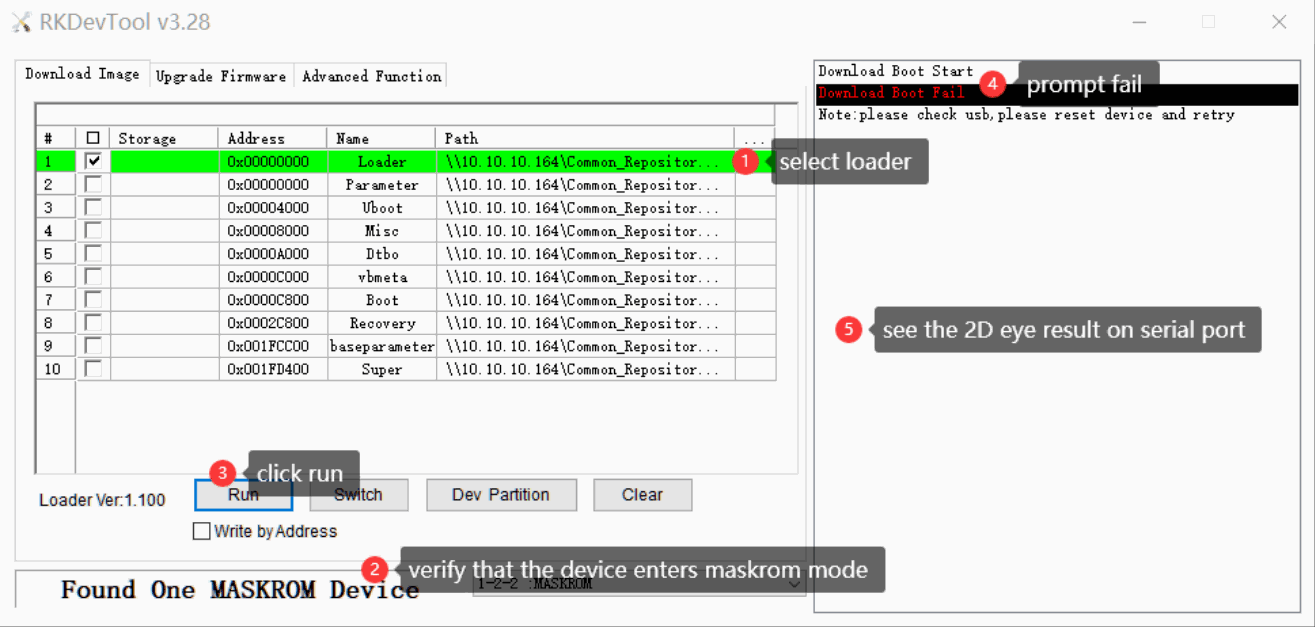
The loader would be downloaded successfully in loader mode. So it will scan 2D eye and then stop every time it boots, and the result is also output via serial port. The boot cannot enter the system normally, please enter maskrom mode to download normal loader to recover.
4.1.2.1 Result analysis
The delay of each step is printed at the beginning of the 2D eye log, the unit is fs (0.001ps). For example, “Unit: 1913 fs” in the first row of the figure below means each step is 1.913 ps.
The second row ‘margin: rx:22-8,tx:26-32’ which means that the setup/hold time margin in the read direction at least needs 22step/8step respectively. The setup/hold time margin in the write direction at least needs 26step/32step respectively. This value has been converted from ps to the step unit on the software eye diagram according to the frequency.As shown in the figure below, the minimum setup and hold time requirement of the rx signal is circled on the rx dq0 eye diagram with ‘|’ according to the setup time 22step, hold time 8step. The ‘[33 ~ -1 ~-35]’ on the right side means that the setup time has 33steps and the hold time has 35steps under this vref. This shows that compared with the minimum 22step/8step margin required by rx, the setup time has an additional 33-22=11step margin, and the hold time has an additional 35-8=27step margin.
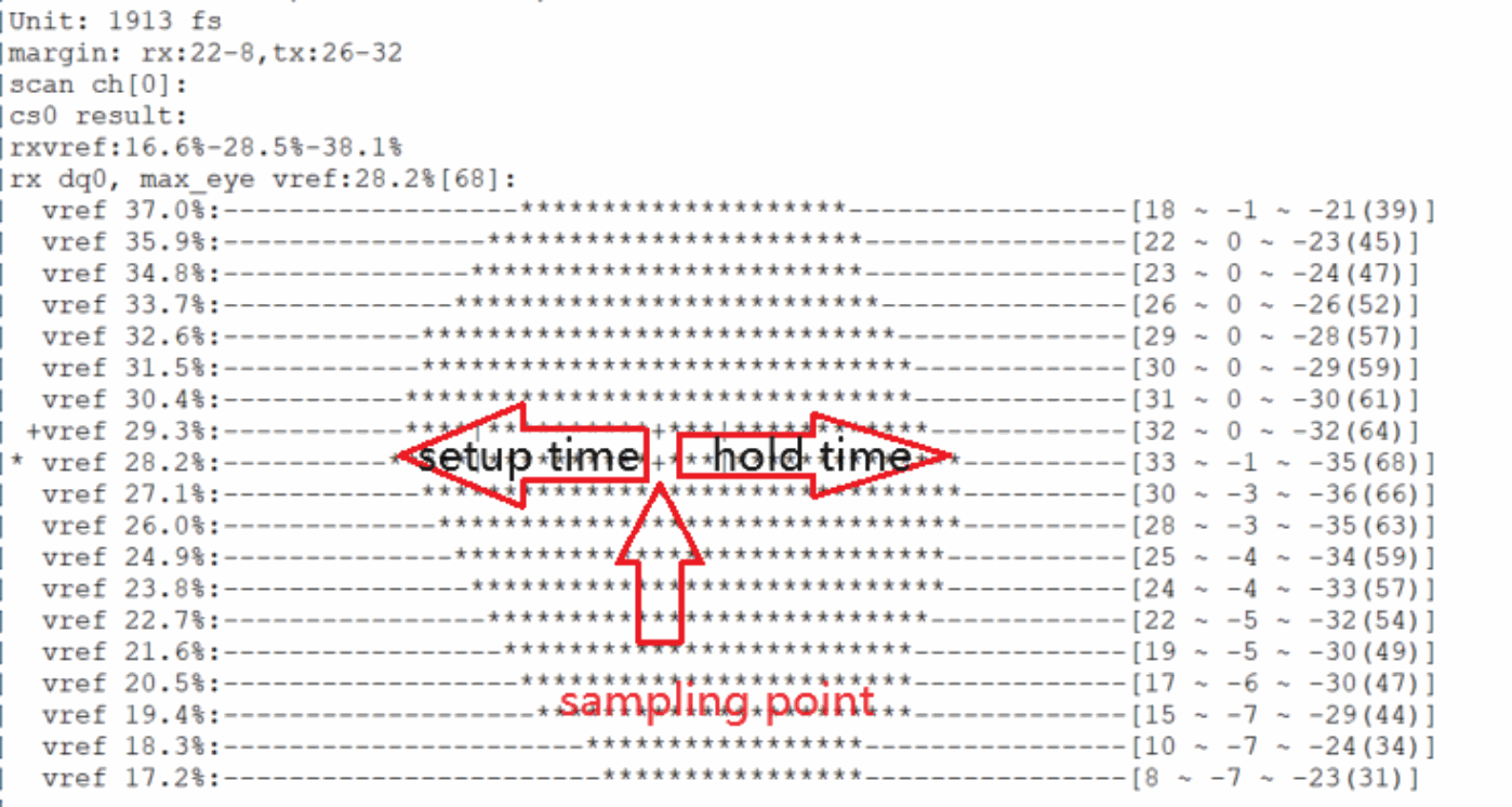
The figure above shows a single DQ eye result.
In the left, “vref” corresponds to the eye width at this reference voltage. The “*” before “vref” indicates the widest eye width is at this reference voltage, and the “+” is the reference voltage used by the current firmware. “vref” value is not accurate, the actual internal value will be the available value closest to this value, for example, 30.4% in the above figure, the actual internal available value is 30.2%, then the actual effective value is 30.2%.
In the middle, “-“ is invalid phase point. “” is valid phase point. “+” is the default sampling point. The ‘|’ range is the minimum margin range required for the actual setup/hold time. ‘+’ to the leftmost ‘’ is the setup time margin of the signal, and ‘+’ to the rightmost ‘*’ is the hold time margin of the signal. When the actual valid eye diagram is pressed to the point within the ‘|’ range, it will be replaced by ‘o’. The appearance of ‘o’ indicates that the signal margin is insufficient. As shown below:
Source typography: the PDF itself has two empty quoted markers in this paragraph. The final sentence uses
*, and the corresponding Chinese paragraph also uses*. The Russian translation reads these two markers as*with this explicit editorial attribution; verify against the tool output.
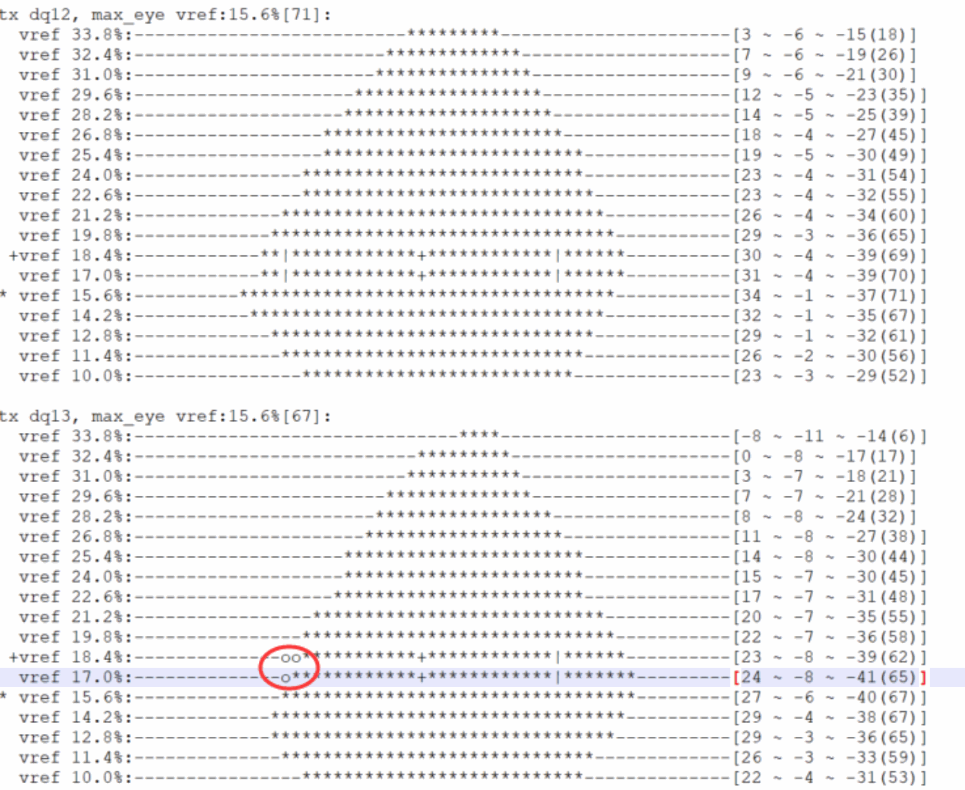
In the right, datas in “[]” from left to right are left eye width boundary, middle value, right eye width boundary, total eye width.
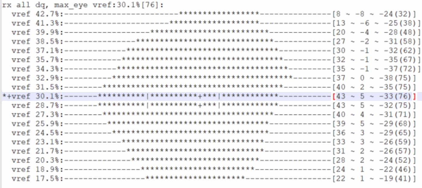
The figure above shows the eye results for all DQ merged.
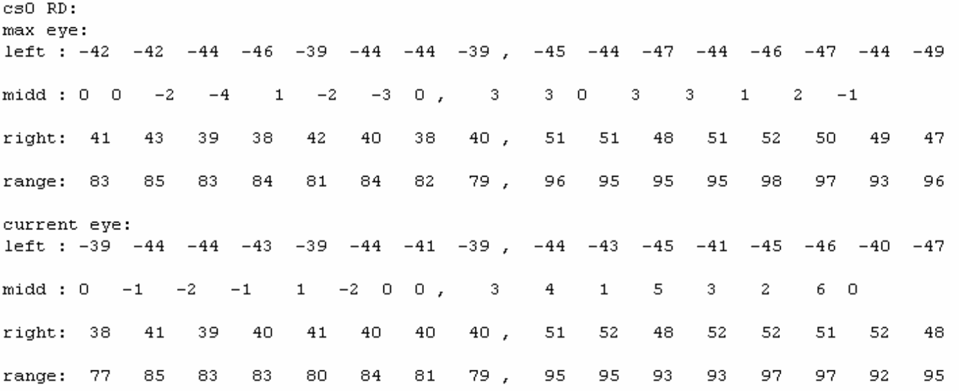
Editable screenshot transcription (original fields and values):
| cs0 RD | Field | 0 | 1 | 2 | 3 | 4 | 5 | 6 | 7 | 8 | 9 | 10 | 11 | 12 | 13 | 14 | 15 |
|---|---|---|---|---|---|---|---|---|---|---|---|---|---|---|---|---|---|
| max eye | left | -42 | -42 | -44 | -46 | -39 | -44 | -44 | -39 | -45 | -44 | -47 | -44 | -46 | -47 | -44 | -49 |
| max eye | midd | 0 | 0 | -2 | -4 | 1 | -2 | -3 | 0 | 3 | 3 | 0 | 3 | 3 | 1 | 2 | -1 |
| max eye | right | 41 | 43 | 39 | 38 | 42 | 40 | 38 | 40 | 51 | 51 | 48 | 51 | 52 | 50 | 49 | 47 |
| max eye | range | 83 | 85 | 83 | 84 | 81 | 84 | 82 | 79 | 96 | 95 | 95 | 95 | 98 | 97 | 93 | 96 |
| current eye | left | -39 | -44 | -44 | -43 | -39 | -44 | -41 | -39 | -44 | -43 | -45 | -41 | -45 | -46 | -40 | -47 |
| current eye | midd | 0 | -1 | -2 | -1 | 1 | -2 | 0 | 0 | 3 | 4 | 1 | 5 | 3 | 2 | 6 | 0 |
| current eye | right | 38 | 41 | 39 | 40 | 41 | 40 | 40 | 40 | 51 | 52 | 48 | 52 | 52 | 51 | 52 | 48 |
| current eye | range | 77 | 85 | 83 | 83 | 80 | 84 | 81 | 79 | 95 | 95 | 93 | 93 | 97 | 97 | 92 | 95 |
To check all single DQ eye results, the figure above summarizes all single DQ eye results.
“max eye” lists the left eye width boundary, the middle value, the right eye width boundary and the total eye width of the widest eye width (the vref marked to by “+”) of all DQ. From left to right are values of DQ0, DQ1…
“current eye” lists the eye width results of the vref currently used (the vref marked to by “*”). Print format similar to “max eye”.
Source conflict: the earlier paragraph assigns * to maximum-width Vref and + to current Vref, while the max/current explanation here reverses these symbols. Both statements are retained; verify the actual tool version and output.
Final result: “all result: pass” will be printed at the end of the eye diagram log, indicating that all dq margins meet the requirements, otherwise “all result: err” will be printed.
4.2 Scan 1D eye
Please scan 2D eye first for platforms that support 2D eye, because the dimension of vref is added. 1D eye is used unless special requirements exist.
4.2.1 Available platforms
RV1109, RV1126, RK3566, RK3568, RK3528, RK3562
4.2.2 How to use
4.2.2.1 Preliminary preparation
1. Check DDR bin version (RV1126 needs V1.09 or above, RK3568/RK3566 needs V1.07 or above). If the version is too low, please update rkbin project.
2. Before compiling the U-Boot project, open menuconfig under the project root directory, enter “Command line interface”, configure “Enable ddr test tool” and save the compilation configuration (Rockchip DDR DQ eye tool is integrated in DDR Test Tool).

Editable screenshot transcription (original fields and values):
[ ] Enable memtester for ddr
[*] Enable ddr test tool
    Misc commands --->
3. Compile the U-Boot project and download Loader and uboot (please refer to the relevant chapter in the UBOOT document for details).
4. Connect the serial port of the board to be tested to the host computer, ensure that the board and the host computer can communicate normally through the serial port. When the board is powered on, the host computer presses Ctrl + C for a long time to make the board stay in U-Boot (“<INTERRUPT>” indicates that the board has stayed in U-Boot).
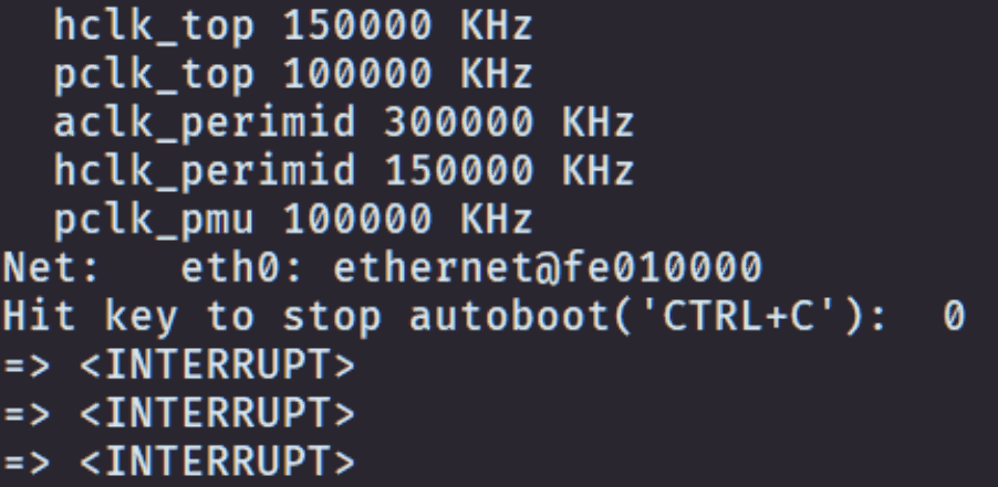
Editable screenshot transcription (original fields and values):
hclk_top 150000 KHz
pclk_top 100000 KHz
aclk_perimid 300000 KHz
hclk_perimid 150000 KHz
pclk_pmu 100000 KHz
Net: eth0: ethernet@fe010000
Hit key to stop autoboot('CTRL+C'): 0
=> <INTERRUPT>
=> <INTERRUPT>
=> <INTERRUPT>
4.2.2.2 View DDR DQ read and write eye in U-Boot
Enter command in U-Boot
ddr_dq_eye <DDR frequency in MHz>
The parameter <DDR frequency in MHz> specifies the DDR clock frequency at which you want to view DQ eye, in MHz, and defaults to the highest frequency when left blank.
Example: View DQ eye when DDR clock frequency is 1056MHz, enter command
ddr_dq_eye 1056
Example: View DQ eye of DDR at highest clock frequency, enter command
ddr_dq_eye
4.2.2.3 Result analysis
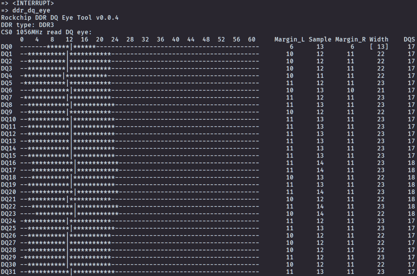
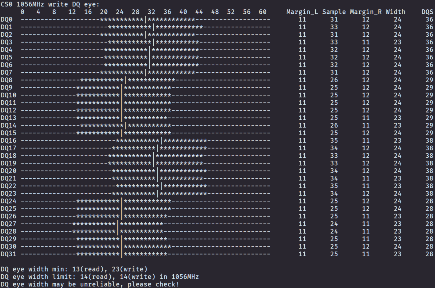
The tool displays tool version, DDR type and frequency at first
The tool displays read eye and write eye of each CS
In the eye diagram, the position of “-“ mark is located outside the eye, the position of “*” mark is located inside the eye, and the the position of “|” mark is the sampling point
On the right, the left margin and right margin (Margin_L, Margin_R), sample position, eye width are displayed. The square brackets mark the eye width that does not meet the minimum eye width limit (as shown in the figure read eye DQ0)
The tool displays the minimum eye width for the read eye and the write eye at the end, as well as the minimum eye width limit (select similar frequency)
4.2.3 DDR DQ min eye width limit
Based on DEMO testing and related project experience, this document limits the minimum reading and writing eye width of DDR DQ. If the minimum read or write eye width does not meet this limit, DDR operation may be unstable.
Meeting the minimum eye width limit of DDR DQ can only indicate that the eye width of DDR DQ is relatively reliable under the current design. However, it does not mean that there must be no other problems in the relevant design of DDR. Please conduct further reliability test according to actual use requirements.
4.2.3.1 RV1126
| DDR type | DDR CLK frequency | Min read eye width limit | Min write eye width limit |
|---|---|---|---|
| LPDDR4 | 1056MHz | 12 | 13 |
| LPDDR4 | 924MHz | 15 | 15 |
| DDR4 | 1056MHz | 13 | 9 |
| DDR4 | 924MHz | 15 | 11 |
| LPDDR3 | 1056MHz | 15 | 13 |
| LPDDR3 | 924MHz | 16 | 15 |
| DDR3 | 1056MHz | 14 | 14 |
| DDR3 | 924MHz | 17 | 17 |
4.2.3.2 RK3568/RK3566
| DDR type | DDR CLK frequency | Min read eye width limit | Min write eye width limit |
|---|---|---|---|
| LPDDR4 | 1560MHz | 25 | 24 |
| LPDDR4 | 1184MHz | 30 | 29 |
| DDR4 | 1560MHz | 30 | 22 |
| DDR4 | 1184MHz | 32 | 26 |
| LPDDR3 | 1184MHz | 34 | 25 |
| LPDDR3 | 1056MHz | 39 | 28 |
| DDR3 | 1184MHz | 32 | 31 |
| DDR3 | 1056MHz | 39 | 34 |
5. Chapter-5 Rockchip DDR Bandwidth Tool Usage Guide
5.1 Terminology Explanation
The main terms involved in this document are explained as follows:
monitor: A function that monitors and collects statistics on various DDR commands.
5.2 Tool Acquisition
https://redmine.rock-chips.com/documents/49 -> DDR Related Materials_VerX.XX.7z -> Tools ->DDR Bandwidth Tool
5.3 Platform Support
You can obtain the supported platforms through the following command:
# rk-msch-probe_vx.xx -h
The following information will be printed (please check the tool version for the specific supported platforms):
Usage: [-c chip_name -d msecs -f freq -h help]
-c <chip_name>:
'rk312x' include rk3126,rk3128 and px3se
'rk322x' include rk3128h,rk3228a,rk3228b and rk3229
...
[option] -d <msecs>: Sets the sampling interval in milliseconds.
[option] -f <freq>: Specifies the mean current DDR frequency in MHz.
[option] -h: Displays help information.
5.4 Parameter Description
The DDR bandwidth test tool (rk_msch_probe_vx.xx) supports the following parameters:
-c: Chip name. After confirming that the current platform is supported, enter the chip name, e.g., rk3326.
-d: Monitoring interval time, in ms, optional. If not specified, the default is 1000ms.
-f: The current DDR frequency, in MHz, optional. During each monitoring time segment, the tool will attempt to obtain the DDR frequency. If it fails, you need to enter the current DDR frequency.
Note that you need to set a fixed DDR frequency first, otherwise the DDR frequency may change which
will cause inaccurate results. -t test_loop: Specify the number of test loops, after which the tool will exit. By default, it runs indefinitely.
-h: Help.
5.5 Usage Conditions
The devfreq governor for DMC cannot be ‘dmc_ondemand’. It is recommended to switch to ‘userspace’ by running the following command:
# echo userspace > /sys/class/devfreq/dmc/governor
Then set a fixed DDR frequency, e.g., set the DDR frequency to 780MHz:
# echo 780000000 > /sys/class/devfreq/dmc/userspace/set_freq
If the following output appears during the tool test, it means that the above usage conditions are not met:
Error: The DDR monitor time gets error!!!
Please check the devfreq governor is not 'dmc_ondemand'!!!
For example:
# cat sys/class/devfreq/dmc/governor
# dmc_ondemand
Please switch the devfreq governor to others, such as 'userspace'.
For example:
# echo userspace > /sys/class/devfreq/dmc/governor
Delete the result of this time!
5.6 Output Explanation
Executing rk_msch_probe_vx.xx will monitor and print the DDR bandwidth and utilization.
The output for general platforms is as follows:
V1.06_20200629
ddr freq: 928Mhz
CH0:
ddr monitor statistics:
ddr load = 3251.23MB/s(43.76%) [RD:1859.93MB/s(25.03%), WR:1391.30MB/s(18.72%), ACT(access :
active): 3.34, srex:0.54%, pdex:1.27%, clkstp:0.00%, lp:1.81%]
The output for RK3588 is as follows:
ddr freq: 2133Mhz
===========ALL=============CH0===============CH1==============CH2===============CH3========
LOAD: 4.51MB/s(0.03%), 1.23MB/s(0.04%), 1.13MB/s(0.03%), 1.16MB/s(0.04%),
 1.00MB/s(0.03%)
RD: 2.57MB/s(0.02%), 0.74MB/s(0.02%), 0.65MB/s(0.02%), 0.67MB/s(0.02%),
 0.51MB/s(0.02%)
WR: 1.94MB/s(0.01%), 0.49MB/s(0.02%), 0.48MB/s(0.01%), 0.49MB/s(0.02%),
 0.48MB/s(0.01%)
===========================================================================================
Explanation of the statistics:
| Output | Explanation |
|---|---|
| ALL | Total bandwidth statistics for all channels. |
| CHx | Bandwidth statistics for DDR channel x. |
| recorded LOAD (max, min, avg) |
For all DDR banks, the maximum, minimum, and average bandwidth and load recorded while running this tool. |
| load/LOAD | For all DDR banks, the bandwidth and load of this channel. |
| RD | For all DDR banks, the bandwidth and percentage of DDR read. |
| WR | For all DDR banks, the bandwidth and percentage of DDR write. |
| PRE | For all DDR banks, the percentage of precharge commands out of the total number of commands. Precharge and active commands appear in pairs, and there is no actual hardware statistics, so the active command statistics result is used directly. |
| ACT(access : active) |
For all DDR banks, the average number of reads/writes after each DDR active command. The higher the value, the more consecutive the DDR address access, which is better. |
| srex | The percentage of time the DDR is in self-refresh state. |
| pdex | The percentage of time the DDR is in power down state. |
| clkstp | The percentage of time the DDR is in clock stop state. |
| srpdex | The percentage of time the DDR is in self-refresh power down state. |
| dsmex | The percentage of time the DDR is in Deep Sleep Mode state. |
| lp/ LOW POWER | The percentage of time the DDR is in low power state (low power state includes self-refresh, power down, and clock stop, etc.). |
5.7 FAQ
1)In case of an abnormal output that “/dev/mem” does not exist during usage, the output will be:
rk3568:/ # rk-msch-probe_vx.xx -c rk356x
open /dev/mem error: No such file or directory
This error occurs because the CONFIG_DEVMEM option is disabled in the kernel configuration, preventing the tool from accessing the device registers.
Solution 1: In the kernel, add CONFIG_DEVMEM=y to the corresponding config file, such as android-11.config, and recompile the firmware.
Solution 2: In the kernel, run make menuconfig , search for DEVMEM , enable it, and recompile the kernel (be careful not to overwrite the config).
Symbol: DEVMEM [=y]
Type : bool
Prompt: /dev/mem virtual device support
Location:
    -> Device Drivers
(1) -> Character devices
  Defined at drivers/char/Kconfig:10
...
[*] /dev/mem virtual device support
...
6. Chapter-6 Rockchip DDR_UserTool (DDR Soldering Inspection Tool) User Guide
6.1 Overview
DDR_UserTool is a tool for DDR soldering inspection.
This tool is released at https://redmine.rock-chips.com/documents/49, DDR相关资料_Verx.xx.7z->工具- >DDR_UserTool_vx.xx.
The version number of DDR_UserTool may remain unchanged for a long time, but the internal configuration files may be updated due to reasons such as supporting new platforms. Therefore, for each new project, it is necessary to obtain the latest version of DDR_UserTool from Redmine.
6.2 Testing Steps
6.2.1 Configure DDR_UserTool to English version
Open resource/config.ini, change “Selected=1” to “Selected=2” to set the language to English.
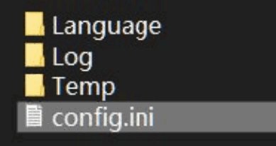
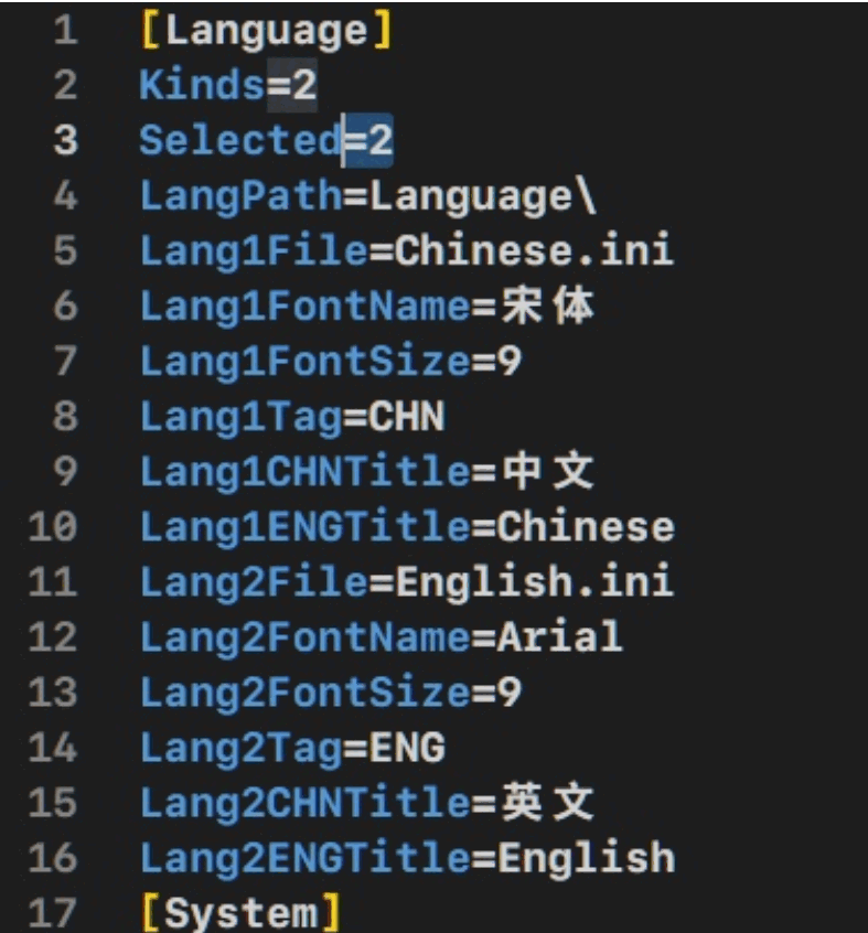
Editable screenshot transcription (original fields and values):
[Language]
Kinds=2
Selected=2
LangPath=Language\
Lang1File=Chinese.ini
Lang1FontName=宋体
Lang1FontSize=9
Lang1Tag=CHN
Lang1CHNTitle=中文
Lang1ENGTitle=Chinese
Lang2File=English.ini
Lang2FontName=Arial
Lang2FontSize=9
Lang2Tag=ENG
Lang2CHNTitle=英文
Lang2ENGTitle=English
[System]
6.2.2 Open DDR_UserTool.exe
Note: For Windows 7, right-click and select “Run as Administrator.”
6.2.3 Select TestFile
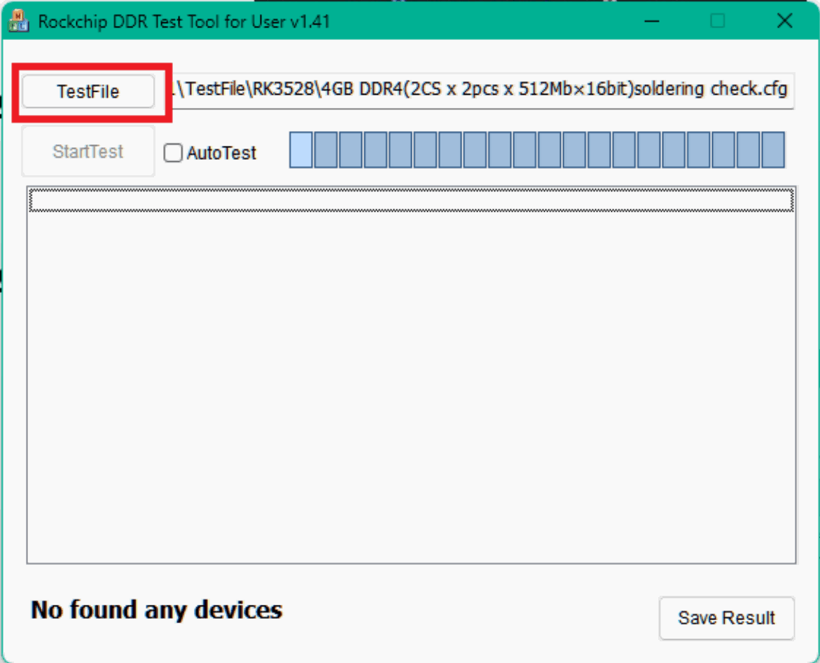
The TestFile is located in the “TestFile” folder under the tool directory, with the file extension .cfg. Please select the corresponding TestFile based on the target platform and DDR capacity information.
Please note:
DDR4 x16 DDP (Dual Die Package) chips should be treated as two x8 chips. Example: If the machine is originally “4GB DDR4(1CS x 2pcs x 1Gb×16bit)”, but uses DDR4 x16 DDP chips, TestFile corresponding to “4GB DDR4(1CS x 4pcs x 1Gb×8bit)” should be selected. For how to identify DDR4 x16 DDP chips, refer to the section “How to Identify DDR4 x16 DDP Chips”.
The TestFiles for LPDDR4 and LPDDR4X are not interchangeable.
For DDR3L, use the TestFile corresponding to DDR3.
6.2.4 Sign TestFile
This step is only applicable to secure-boot machines. Machines without secure-boot skip this step.
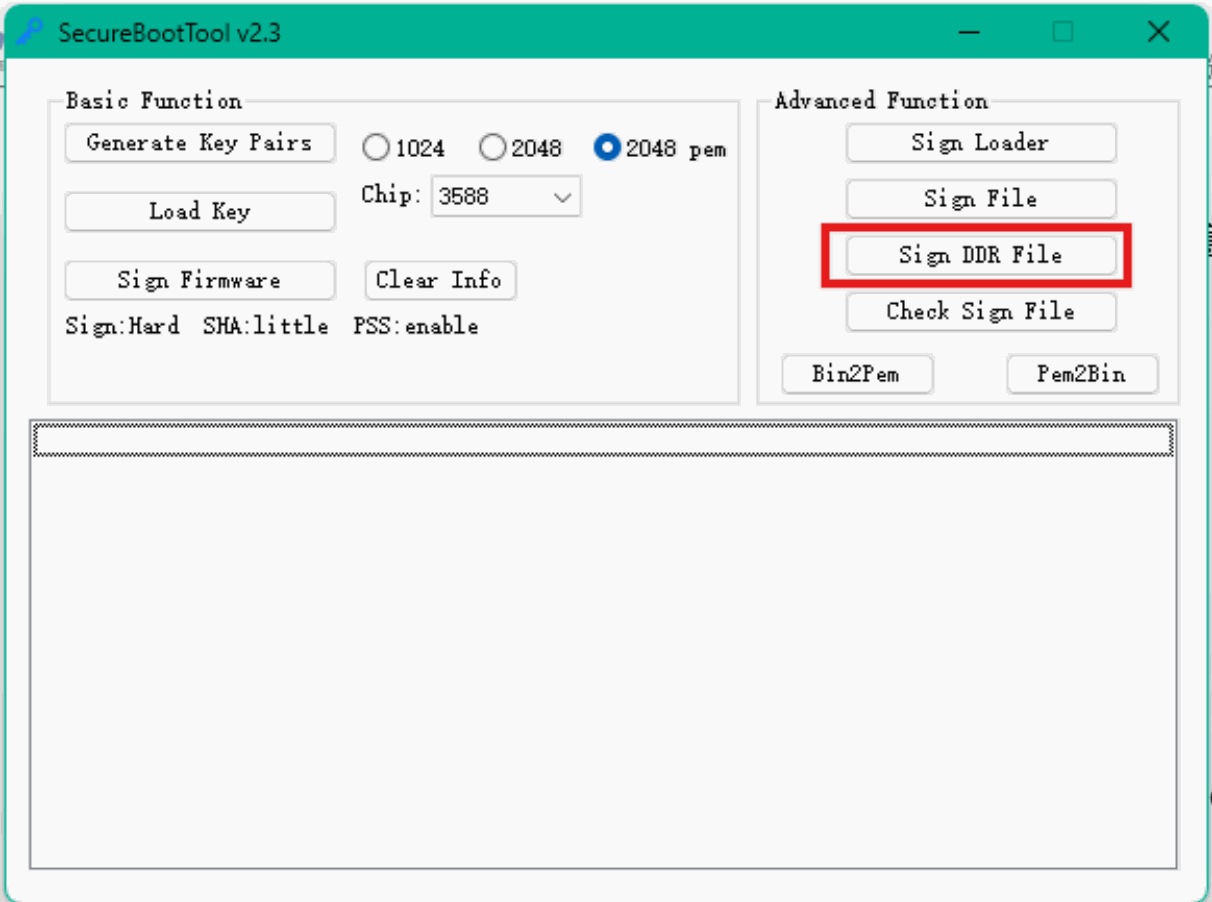
Sign the TestFile with SecureBootTool to test the secure-boot machines, SecureBootTool is also available at: ht tps://redmine.rock-chips.com/documents/49. After configuring Chip, Key and other options, click “Sign DDR File” to sign the TestFile. Please refer to SecureBootTool_UserManual for details.
6.2.5 Put the Target Machine into Test State
Connect the OTG port of the target machine. If possible, it is also recommended to connect the serial port.
There are several methods to put the target machine into test state:
Machines that have not been programmed with any firmware
These machines are inherently in Maskrom state and can be tested directly.
Put the machine into Maskrom state
Short-circuit the CLK and GND of the storage device during power-on to put the machine into Maskrom state. For specific pins to short-circuit, refer to the schematic released by RK. Generally, there are reserved button or TP for entering Maskrom mode.
Put the machine into Loader mode
After the target machine enters the test state, the tool will display “Found one device”
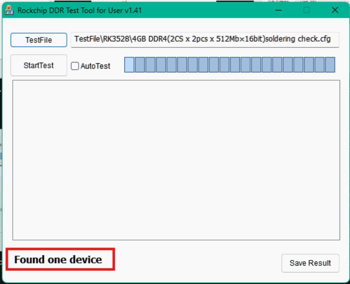
6.2.6 Start Testing
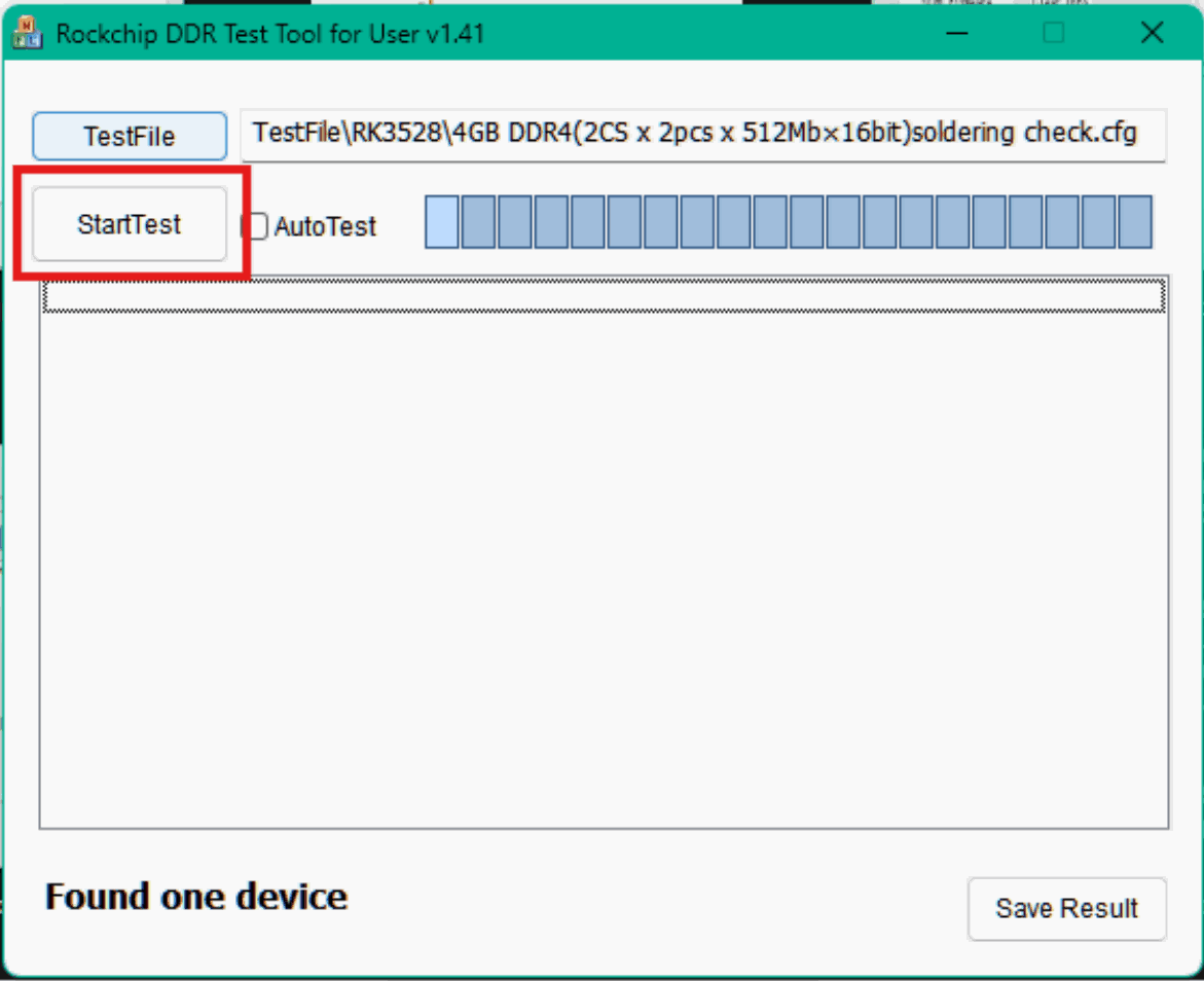
Click “StartTest”. The progress bar will begin to scroll, and the test log will be displayed synchronously on the tool interface. The test usually takes less than 2 minutes to complete.
If “AutoTest” is selected, the test will be automatically performed when a device is connected.
6.2.7 Obtain Test Results
6.2.7.1 Test PASS
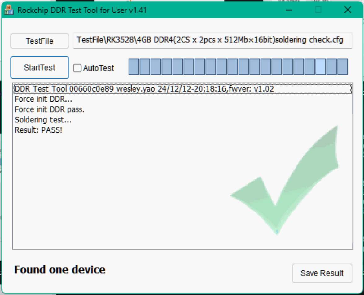
6.2.7.2 Test FAIL
Based on the error messages printed by the tool, re-solder the faulty DDR chips and SoC. Refer to the section “Correspondence between Error Messages and Actual Hardware Signal Lines” to identify the specific faulty signal lines.
For machines that fail testing, retesting is mandatory after repair and must continue until they pass testing.
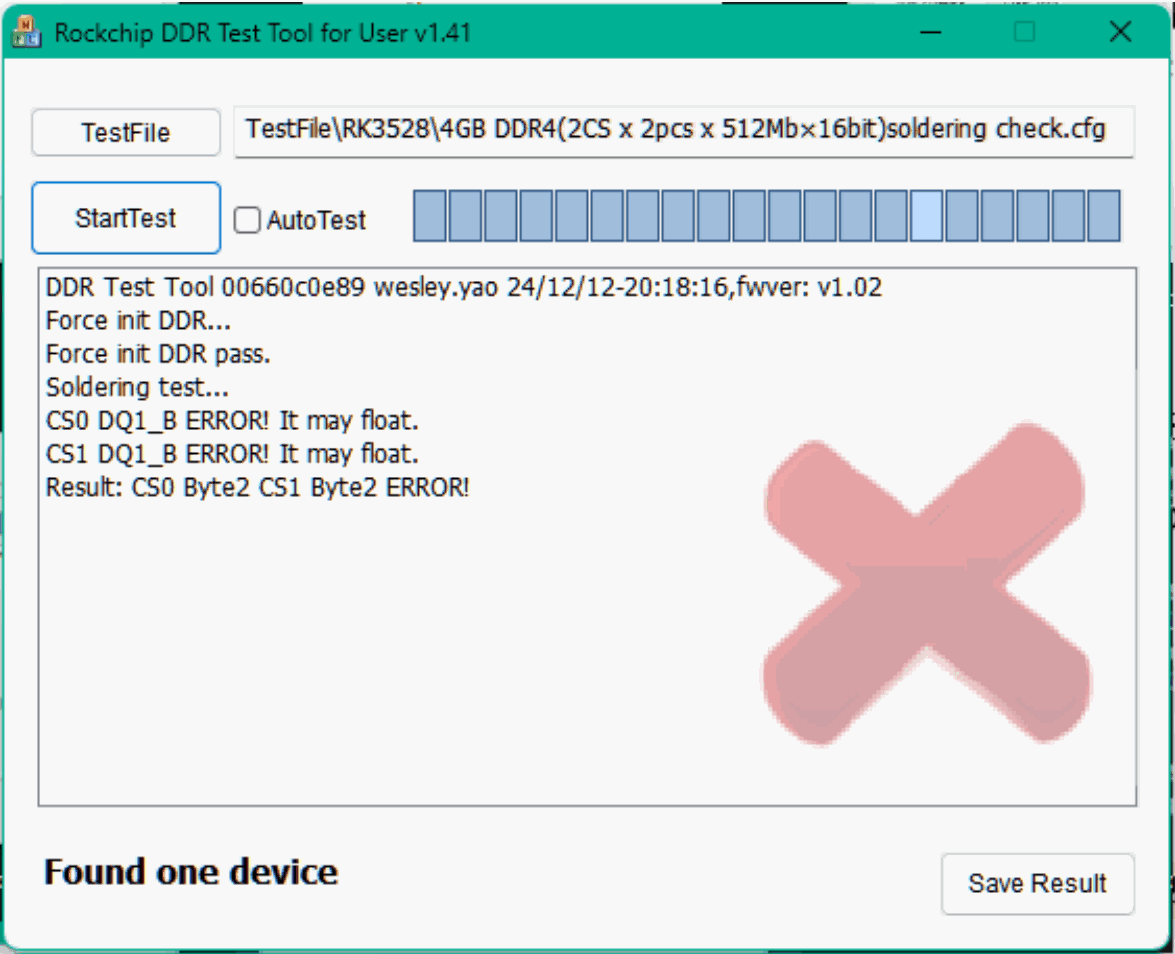
6.2.7.3 Test Interrupted
Refer to the section “Reasons for Test Interruption” for troubleshooting.
6.3 FAQ
6.3.1 Can DDR_UserTool test DDR stability?
No! DDR_UserTool currently only provides DDR soldering inspection functionality. For DDR stability testing, please refer to the section “DDR Verification Process” in this document.
6.3.2 Can DDR_UserTool detect soldering issues for all pins?
No! DDR_UserTool provides a fast and convenient DDR soldering inspection solution through software, but software has limitations and cannot detect all DDR-related pins, nor can it detect pins of other modules.
Generally, soldering issues for DDR DQ and most CA pins can be detected. Soldering issues for power pins and CKE, ODT pins cannot be detected.
6.3.3 How to Identify DDR4 x16 DDP Chips
1. Check the schematic. If the M9 pin of the DDR4 chip is connected to the BG1 pin on the SoC side, it is an x16 DDP chip. If the M9 pin is connected to VSS, it is not an x16 DDP chip.
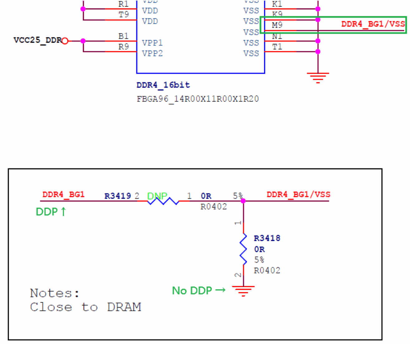
2. Check the Loader log of the normal machine booting. In the DDR capacity information log, if “Die BW=8” is displayed, it confirms the use of the x16 DDP chip.
3. Check the chip datasheet. Look for explicit statements indicating it is a DDP (Dual Die Package) chip. Alternatively, if the M9 pin is BG1, it is an x16 DDP chip; if it is VSS, it is not.
6.3.4 Cannot find the TestFile for the machine
Check for updates.
If a newer platform does not yet have a corresponding TestFile, please wait for the tool update.
For platforms that have released TestFiles, common DDR capacity information usually has corresponding TestFiles. There are many TestFiles, so please double-check. If the DDR capacity information is special and the corresponding TestFile cannot be found, please ask on Redmine.
6.3.5 Reasons for Test Interruption
1. Not “Run as Administrator” on Windows 7
2. Incorrect TestFile selection (e.g., platform mismatch, DDR type mismatch, DDR capacity information mismatch)
3. Machine did not re-enter test state and was tested repeatedly
4. The TestFile was not signed for secure-boot machines
5. Tool and TestFile not updated
6. Machine power supply issue (e.g., insufficient USB power)
7. USB connection issue, try replacing the cable or using a different computer for testing
8. If the machine is in Loader mode, try Maskrom mode for testing
6.3.6 Correspondence between Error Messages and Actual Hardware Signal Lines
The CA bus is not allowed to be swapped, and the correspondence is generally unambiguous.
If there are errors in DQ in the error messages, they correspond to the pin names on the SoC side. Pay attention to the common part of the pin names, not the part corresponding to the DDR type. For example, the following figure is a part of the RK3528 DDR4 schematic, the common part of the pin names is highlighted in the green box; if the tool reports DQ1_B error, it means that there is an issue with the signal line corresponding to the DDRPHY_B_DQ1 pin on the SoC, which is the DDR4_DQU0_B signal line.
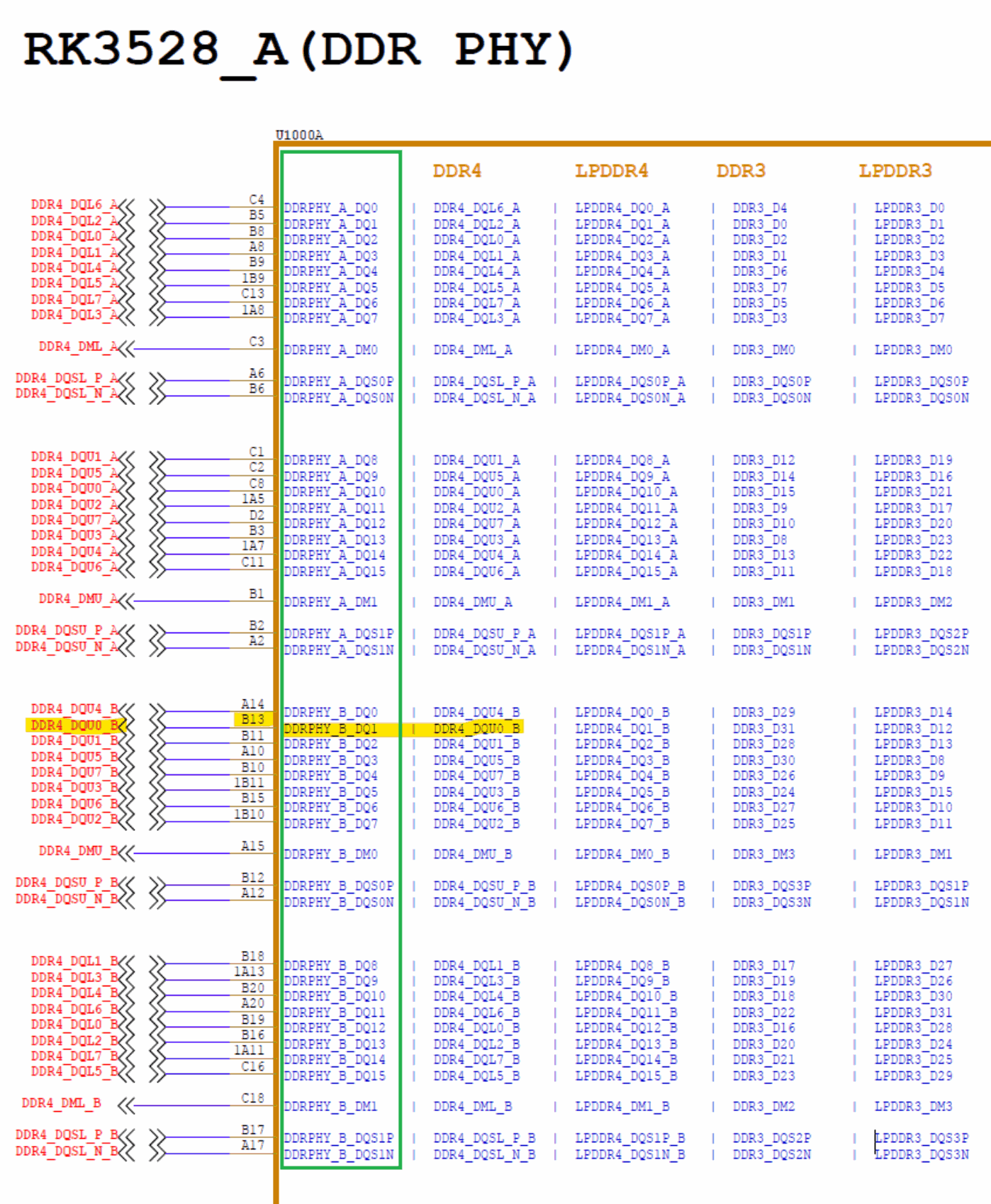
6.3.7 DDR_UserTool Test FAIL, but X-ray Shows No Soldering Issues
X-ray may not detect all soldering issues. It is still recommended to try re-soldering the DDR chips and SoC.
6.3.8 Re-soldered, but Still Test FAIL
1. Incorrect TestFile selection, or tool and TestFile not updated
2. Possible cold solder joints on both the DDR chip side and SoC side, both sides need re-soldering
3. PCB process issues, such as non-conductive traces
4. Other non-DDR-soldering issues (DDR chip issues, hardware design issues, power supply issues, etc.)
6.3.9 Large Number of Machines Test FAIL
1. Incorrect TestFile selection, or tool and TestFile not updated
2. Issues with the assembly factory or PCB process
3. Other non-DDR-soldering issues (DDR chip issues, hardware design issues, power supply issues, etc.)
6.3.10 Further Questions Need to Be Asked on Redmine
To improve communication efficiency, in addition to clearly describing the problem, please provide the following information:
1. DDR PN and datasheet
2. Number of DDR chips mounted on the board, preferably with a schematic diagram
3. TestFile used
4. Proportion of abnormal machines
5. DDR_Test_Log.txt under the tool directory, corresponding Log file in resource\Log, and serial port log during testing (if there are normal machines, please also provide these logs from normal machines for analysis)
6. Serial port log during power-on (if there are normal machines, please also provide the power-on log from normal machines for analysis)
7. Chapter-7 Rockchip Developer Guide HAL DDR ECC
7.1 Applicability
This document is only applicable to systems with HAL and is not applicable to Linux systems.
7.2 Terminology Explanation
| Abbreviation | Description |
|---|---|
| ECC | Error Correcting Code |
| SEC ECC | Single Bit Single Error Correction Code |
| DED ECC | Double Error Detection Error Correction Code |
| DDR | Double Data Rate SDRAM |
| CE | Correctable Error |
| UE | Uncorrectable Error |
| cs | chip select |
| Row | Refers to DDR row address |
| Chip ID | Refers to DDR chip id, not activated at present, please disregard |
| BankGroup | Refers to DDR4 Bank Group address, ignore for other DDR types |
| Bank | Refers to DDR bank address |
| Col | Refers to DDR column address |
| Bit position | Refers to the bit position corrected by CE |
7.3 Introduction
The ECC stands for Error Correcting Code, while DDR ECC is utilized for error detection and correction of DDR data. The RK3568 supports SideBand ECC, which adds a dedicated DDR channel for storing ECC data alongside the DDR data channel. The ECC has the ability to correct 1-bit errors and detect 2-bit errors, known as SEC/DED ECC (Single Error Correction/Double Error Detection).
7.4 Enable DDR ECC
1. Enable ECC: The DDR ECC is automatically enabled when a chip is attached to DDR_ECC_DQ0-7.
2. Function of DDR_ECC_DQ0-7: ECC uses 32-bit DQ data + 7-bit ECC data. DDR_ECC_DQ0-7 stores the ECC data calculated from DQ0-DQ31. Hence, an additional chip is needed to store the ECC data.
3. Requirements for the additional ECC chip: The additional ECC chip must match the type, Row, Column, and Bank of the chips attached to DQ0-31.
4. Supported DDR types: All DDR types support ECC.
7.5 Getting DDR ECC Information in HAL
The specific error checking and correction behavior of DDR ECC is accomplished by IP design. Software can obtain relevant information.
7.5.1 Configuration
In the hal_conf.h file of the project, enable the DDR ECC module. For example, as for rk3568, add the following code in project/rk3568/src/hal_conf.h .
#define HAL_DDR_ECC_MODULE_ENABLED
7.5.2 Code and API
lib/hal/src/hal_ddr_ecc.c
lib/hal/inc/hal_ddr_ecc.h
/* Initialize DDR ECC related information */
HAL_Status HAL_DDR_ECC_Init(struct DDR_ECC_CNT *p);
/*
 * Get cumulative statistical information of DDR ECC, including the number of single-bit
 * correctable errors and double-bit detectable but uncorrectable errors
 */
HAL_Status HAL_DDR_ECC_GetInfo(struct DDR_ECC_CNT *p);
7.5.3 Example Usage
Upper-layer software can obtain DDR ECC information through two methods: software polling and hardware interrupts.
Software polling method
Example:
struct DDR_ECC_CNT eccInfo;
void HAL_DDR_ECC_TEST_POLL(void)
{
    uint32_t cpuID;
    cpuID = HAL_CPU_TOPOLOGY_GetCurrentCpuId();
    if (cpuID == 0) { /* Use a CPU, thread, or other method to
initialize and poll DDR ECC status */
        HAL_DDR_ECC_Init(&eccInfo);
        while (1) { /* After initializing DDR ECC information,
poll to get DDR ECC information */
            HAL_DDR_ECC_GetInfo(&eccInfo); /* Cumulative CE and UE counts are stored
in the eccInfo structure */
            HAL_DelayMs(50);/* Polling interval, or other APIs to let the CPU idle */
        }
    }
}
Hardware interrupt method
Example:
struct DDR_ECC_CNT eccInfo;
void HAL_DDR_ECC_IRQHandler(uint32_t irq)
{
    HAL_DDR_ECC_GetInfo(&eccInfo);
}
void HAL_DDR_ECC_TEST_INT(void)
{
    uint32_t cpuID;
    cpuID = HAL_CPU_TOPOLOGY_GetCurrentCpuId();
    if (cpuID == 0) { /* Use a CPU, thread, or other method to initialize DDR ECC
related */
        HAL_DDR_ECC_Init(&eccInfo);
        HAL_GIC_SetHandler(DDR_ECC_CE_IRQn, HAL_DDR_ECC_IRQHandler); /* Attach CE
interrupt service routine */
        HAL_GIC_SetHandler(DDR_ECC_UE_IRQn, HAL_DDR_ECC_IRQHandler); /* Attach UE
interrupt service routine */
        HAL_GIC_Enable(DDR_ECC_CE_IRQn); /* Enable CE interrupt
service */
        HAL_GIC_Enable(DDR_ECC_UE_IRQn); /* Enable UE interrupt
service */
    }
}
If an ECC error is detected, print the acquired ECC information.
# 2 CE (correctable errors) detected
[HAL WARNING] DDR ECC error: CE, 2 errors, the last is in DDR cs 0, Row 0xa0, ChipID
0x0, BankGroup 0x0, Bank 0x5, Col 0x318, Bit position 0x10000000
# 1 UE (uncorrectable error) detected
[HAL ERROR] DDR ECC error: UE, 1 errors, the last is in DDR cs 0, Row 0xa0, ChipID
0x0, bankGroup 0x0, Bank 0x5, Col 0x354
7.6 DDR ECC data poison
There is a method to verify the functionality of DDR ECC. Once DDR ECC data poisoning is enabled, write and read to a specific physical address will trigger DDR ECC CE/UE.
7.6.1 Code and API
lib/hal/src/hal_ddr_ecc.c
lib/hal/inc/hal_ddr_ecc.h
/* Enable DDR ECC error injection */
HAL_Status HAL_DDR_ECC_PoisonEnable(struct DDR_ECC_CNT *p);
/* Disable DDR ECC error injection */
HAL_Status HAL_DDR_ECC_PoisonDisable(struct DDR_ECC_CNT *p);
By default, the DDR ECC data poison is single-bit detectable and correctable errors (CE). To change it to
double-bit detectable but uncorrectable errors (UE), modify as follows:
static HAL_Status DDR_ECC_SMCPoison(uint32_t eccPoisonEn,
                                    struct DDR_ECC_CNT *priv)
{
    ...
    pShareMemCfg->eccPoisonMode = DDR_ECC_UE_DATA_POISON;
    ...
}
7.6.2 Example Usage
struct DDR_ECC_CNT eccInfo;
void DDR_ECC_PoisonTriger(struct DDR_ECC_CNT *priv)
{
    uint32_t volatile *p = NULL;
    printf("DDR_ECC debug: eccPoisonAddr = 0x%llx\n", priv->eccPoisonAddr);
    if (priv->eccPoisonAddr) {
        p = (uint32_t volatile *)priv->eccPoisonAddr;
        *p = 0x5aa5f00f; /* Write to the DDR ECC data poison physical address */
        HAL_DCACHE_CleanInvalidate(); /* If the address attribute is cacheable, flush Dcache
to ensure the write is successful */
        printf("DDR_ECC debug: %p = 0x%x, reread = 0x%x\n", p, *p, *p);
    }
}
void DDR_ECC_GetInfo(void)
{
    HAL_DDR_ECC_GetInfo(&eccInfo);
}
void HAL_DDR_ECC_TEST_POLL(void)
{
    uint32_t cpuID;
    uint32_t i = 10;
    cpuID = HAL_CPU_TOPOLOGY_GetCurrentCpuId();
    if (cpuID == 0) {
        HAL_DDR_ECC_Init(&eccInfo);
        HAL_DDR_ECC_PoisonEnable(&eccInfo);/* Enable DDR ECC data poison, the physical
address for data poison will be saved in eccInfo.eccPoisonAddr */
        while (i) {
            DDR_ECC_GetInfo();
            HAL_DelayMs(50);
            i--;
            if (i == 5) {
                DDR_ECC_PoisonTriger(&eccInfo); /* Trigger DDR ECC error */
            }
        }
        HAL_DDR_ECC_PoisonDisable(&eccInfo);
    }
}
7.7 Notes
1. The DDR ECC will utilize the DDR space [0x100000, 0x1F0000]. If this space is not mapped in MMU, mapping needs to be added.
--- a/lib/CMSIS/Device/RK3568/Source/Templates/mmu_rk3568.c
+++ b/lib/CMSIS/Device/RK3568/Source/Templates/mmu_rk3568.c
@@ -41,6 +41,8 @@ void MMU_CreateTranslationTable(void)
     // Define dram address space
    ...
+ MMU_TTSection(MMUTable, 0x100000, 0x100000 >> 20, Sect_Normal);
    ...
2. The physical address space for data poison may not be mapped in HAL, mapping needs to be added. For example, if the address is 0x13576c20, add the following modification.
--- a/lib/CMSIS/Device/RK3568/Source/Templates/mmu_rk3568.c
+++ b/lib/CMSIS/Device/RK3568/Source/Templates/mmu_rk3568.c
@@ -41,6 +41,8 @@ void MMU_CreateTranslationTable(void)
     // Define dram address space
    ...
+ MMU_TTSection(MMUTable, 0x13500000, 0x100000 >> 20, Sect_Normal);
    ...
3. The DED ECC will trigger CPU data abort exception. HAL does not handle it by default, so if you want to print the DDR ECC UE error print, add the following modification.
--- a/lib/CMSIS/Device/RK3568/Source/Templates/GCC/startup_rk3568.c
+++ b/lib/CMSIS/Device/RK3568/Source/Templates/GCC/startup_rk3568.c
@@ -237,6 +237,7 @@ void Reset_Handler(void)
  *----------------------------------------------------------------------------*/
 void Default_Handler(void)
 {
+ DDR_ECC_GetInfo();
     while(1);
 }