
This is a platform reference derived from Rockchip Clock Developer Guide, V1.2.0 (2024-08-02), not an ArmSoM validation report. It covers the documented Rockchip Linux clock framework: RK303X/RK312X/RK322X/RK3288X/RK3328/RK3368/RK3399/RV1108/PX30 on Linux 4.4/4.19/5.10; RV1126 and RK356X on 4.19/5.10; RK3588 and RV1103B on 5.10; and RK3576/RK3506 on 6.1. Apply it to an ArmSoM board only after checking that board’s SoC, released BSP, CRU/PMUCRU map, DTS and boot chain. No frequency, jitter or power result below is an ArmSoM hardware measurement.
The Chinese source is 24 pages and the English source is 24 pages. Chinese source figures are used in Chinese; English figures are used here and in Russian. Cover legal notices, contacts, intended-audience text and revision-history tables have been removed. Editorial notes.
1. Clock-tree model
The clock subsystem is not the Linux timekeeping clock. It is the hierarchical framework that supplies clocks to SoC consumers such as USB and peripheral drivers. A clock tree is built from an oscillator/crystal, PLLs, dividers, multiplexers, gates and consuming hardware blocks. The platform scheme selects PLL settings, parent clocks, dividers and muxes; it differs by SoC.
The usual work flow is: enable or disable a clock, set its rate, and choose its parent. The source locates the implementation in drivers/clk/rockchip/clk-rk3xxx.c; binding IDs in include/dt-bindings/clock/rk3xxx-cru.h or include/dt-bindings/clock/rockchip,rk3xxx-cru.h; SoC-specific handling in drivers/clk/rockchip/clk-xxx.c; and generic APIs under drivers/clk/.
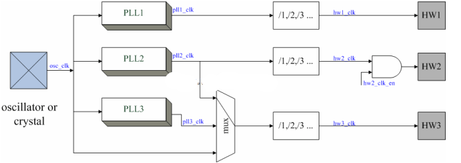
2. PLL, buses and gates
| PLL | Main role in the source | Typical source values |
|---|---|---|
| APLL | CPU (CLOCK_CORE) |
Changes with CPU frequency |
| DPLL | DDR (CLOCK_DDR) |
Changes with DDR requirements |
| GPLL | Bus/peripheral fallback | 594 MHz or 1200 MHz; supports basic 100/200/300/400 MHz outputs |
| CPLL | GMAC/other fallback or LCDC | 400/500/800/1000 MHz in examples |
| NPLL | Other-device fallback or LCDC | 1188 MHz example |
ACLK transports data; PCLK and HCLK normally serve register access. The source gives broad design ranges of 100–300 MHz for ACLK, 50–150 MHz for PCLK, and 37–150 MHz for HCLK. BUS normally contains lower-speed devices such as I2C/I2S/SPI, while PERI commonly serves eMMC/GMAC/USB. This is not a fixed rule: some SoCs give high-demand peripherals independent ACLKs. RK3399 separates high-speed ACLK_PERIHP/HCLK_PERIHP/PCLK_PERIHP from low-speed ACLK_PERILP0/HCLK_PERILP0/PCLK_PERILP0/HCLK_PERILP1/PCLK_PERILP1 for power control.
Gates are parent/child reference-counted. Enabling the leaf automatically walks and enables parents; a parent is shut only once all relevant children are shut. A driver should therefore control its documented leaf clock rather than force a parent gate.
3. Initial clock-tree configuration
After Linux 4.4, the documented initialization route is of_clk_set_defaults(). It reads assigned-clocks, then matches the optional entries in assigned-clock-parents and assigned-clock-rates by position. The three properties must stay one-to-one; a shifted list silently applies an intended setting to the wrong clock.
&cru {
        assigned-clocks = <&cru ACLK_VOP0>, <&cru HCLK_VOP0>,
                          <&cru PLL_GPLL>, <&cru PLL_CPLL>;
        assigned-clock-parents = <&cru VPLL>, <&cru VPLL>,
                                 <&cru GPLL>, <&cru GPLL>;
        assigned-clock-rates = <400000000>, <200000000>,
                               <594000000>, <800000000>;
};
The fragment is abbreviated from the RK3399 source example: use the actual SoC’s binding names and retained complete lists. A clock not enabled by default and not requested by a consumer may be disabled after initialization. The source describes three intentional exceptions:
- Add its name to the SoC
*_critical_clockslist when it must remain enabled. - Use
CLK_IGNORE_UNUSEDon a gate definition when it must not be disabled during unused-clock cleanup; its visible enable count can still be zero. - With kernel 6.1, either use the documented boot arguments
clk_gate.always_on=1 pm_domains.always_on=1to retain all clocks, or useCLK_IS_CRITICALfor a selected definition. Keeping all clocks active trades power for diagnostic safety.
Clock IDs are defined by the SoC binding header. In clk-rk3xxx.c, the common registration macros are GATE (gate register and bit), MUX (parent selector), and COMPOSITE (mux, divider and gate). Do not invent numeric IDs from another SoC.
4. Driver integration and API
Prefer a named DTS clock reference. The source’s TSADC pattern is:
clocks = <&cru SCLK_TSADC>, <&cru PCLK_TSADC>;
clock-names = "tsadc", "apb_pclk";
assigned-clocks = <&cru SCLK_TSADC>;
assigned-clock-rates = <750000>;
#include <linux/clk.h>

dev->pclk = devm_clk_get(&pdev->dev, "tsadc");
dev->clk = devm_clk_get(&pdev->dev, "apb_pclk");
/* devm_clk_get(NULL, "g_p_saradc") is a legacy alternative when DTS has none. */
Relevant APIs are devm_clk_get(), clk_get()/clk_put(), devm_clk_get_optional(), devm_clk_bulk_get(), devm_clk_bulk_get_all(), clk_prepare()/clk_unprepare(), clk_enable()/clk_disable(), clk_prepare_enable()/clk_disable_unprepare(), clk_get_rate(), clk_round_rate() and clk_set_rate() (Hz). Managed and bulk APIs are preferred where applicable.
prepare/unprepare may sleep and must not run in atomic context; enable/disable are atomic operations. The combined prepare/enable pair is convenient only in non-atomic context. Every acquire/enable path needs the matching release/disable path, including probe failure and remove paths:
thermal->num_clks = devm_clk_bulk_get_all(&pdev->dev, &thermal->clks);
if (thermal->num_clks < 1)
        return -ENODEV;
error = clk_bulk_prepare_enable(thermal->num_clks, thermal->clks);
/* ... */
clk_bulk_disable_unprepare(thermal->num_clks, thermal->clks);
5. Debugging
Inspect the runtime tree first:
cat /sys/kernel/debug/clk/clk_summary
cat /sys/kernel/debug/clk_saradc/clk_rate
echo 24000000 > /sys/kernel/debug/clk_saradc/clk_rate
echo 1 > /sys/kernel/debug/clk_saradc/clk_enable_count
echo 0 > /sys/kernel/debug/clk_saradc/clk_enable_count
# Kernel 6.1 source example:
echo 1 > /sys/kernel/debug/clk_saradc/clk_prepare_enable
echo 0 > /sys/kernel/debug/clk_saradc/clk_prepare_enable
Debugfs nodes are build- and kernel-dependent; do not script their existence as a production assumption. The source also documents routing selected clocks to TEST_CLK_OUT, then setting its mux, divider and gate in CRU. For RK3399, the illustrated offsets are CRU_MISC_CON 0x050c, CRU_CLKSEL58_CON 0x01e8, and CRU_CLKGATE13_CON 0x0334, added to the operational base. Confirm the board schematic and SoC TRM before probing an output pin.
6. PLL and clock-design constraints
The source table uses RK3036_PLL_RATE(rate, refdiv, fbdiv, postdiv1, postdiv2, dsmpd, frac). Its formulas are:
VCO  = 24 MHz × FBDIV / REFDIV       (source range: 450–2200 MHz)
FOUT = VCO / POSTDIV1 / POSTDIV2
POSTDIV1 >= POSTDIV2
Example: 24 MHz × 99 / 2 = 1188 MHz, then 1188 / 2 / 1 = 594 MHz. Larger VCO reduces jitter but increases power; a smaller REFDIV shortens PLL lock time. When a target rate is absent, parameters may be calculated automatically, but the source cautions that this may not maximize VCO and is unsuitable where PLL jitter matters.
Display DCLK commonly needs a dedicated PLL because it follows panel resolution. The source maps RK303X/RK312X/RK322X/RK3288X to CPLL, RK3368 to NPLL, RK3399 dual display to CPLL/VPLL, RK3568 three ports to HPLL/VPLL, RK3588 four ports to V0PLL plus two HDMI PHY PLLs, RK3576 three ports to VPLL plus one HDMI PHY PLL, and RK3506 to nearest division for one port. On RK3399, bind the HDMI VOP DCLK to VPLL and the other VOP to CPLL as the source’s DTS example shows; reverse the roles only when the actual display routing requires it.
For I2S, UART and other fractional dividers, the source requires the fractional clock to be 20 times its parent frequency. Missing that relationship creates substantial jitter and frequency error. Ethernet generally needs an exact 50 MHz clock for gigabit Ethernet and 125 MHz for 10-gigabit Ethernet according to the source; use an external crystal if the PLL plan cannot supply the required precision. RK3576/RK3506 PLL references can use original crystal input or added IO input for audio synchronization; this configuration requires SoC-specific BSP documentation.
7. Safe workflow
- Start from the board’s released DTS and clock driver, not a register address copied from another Rockchip SoC.
- Identify consumer, requested rate, acceptable tolerance, parent candidates and all shared consumers.
- Make DTS assignments positionally consistent; use
clk_round_rate()before committing a new rate. - Verify parent, actual rate and enable count through
clk_summary; measure test output only when the pinmux and schematic make it safe. - Test suspend/resume, peripheral traffic, display modes and Ethernet/serial accuracy. Treat any source rate as a target, not a board-level guarantee.