
ArmSoM applicability and source scope
Platform reference for adapting ArmSoM systems, based on CN V1.0.1; no EN PDF. No board, SDK/BSP, kernel or wiring combination has been hardware-validated here. The source scope below is not a claim that every ArmSoM board or kernel supports these features. Check the exact SoC, board schematic, SDK/BSP, kernel driver and pinmux. Commands, patches, logs and measurements are source examples, not ArmSoM test results.
No English PDF was supplied. English/Russian fully translate the Chinese source and use its original Chinese figures, with localized captions.
| Source SoC | Source kernel scope |
|---|---|
| RK3188 | 4.4 |
| RK3288 | 4.4 |
| RK3036 | 4.4 |
| RK312x | 4.4 |
| RK322x | 4.4 |
| RK3368 | 3.10 |
| RK3368 | 4.4 |
| RK3366 | 4.4 |
| RK3399 | 4.4 |
| RV1108 | 3.10 |
| RV1108 | 4.4 |
| RK3228H | 3.10 |
| RK3328 | 4.4 |
| RK3326/PX30 | 4.4 |
| RK3308 | 4.4 |
IO supplies may use 1.8v, 3.3v, 2.5v or 5.0v; some IO supports multiple levels. IO-domain configures the voltage-domain registers according to the actual hardware voltage range. Incorrect settings prevent normal operation. The following source table lists chips requiring configuration; it is not a voltage-tolerance guarantee for any pin.
Editorial notes · ArmSoM documentation · Rockchip Linux
1. Driver file and DTS nodes
1.1 Driver file
Driver location: drivers/power/avs/rockchip-io-domain.c.
1.2 DTS nodes
In kernel 3.10 the DTS nodes are combined:
io-domains {
    compatible = "rockchip,rk3368-io-voltage-domain";
    rockchip,grf = <&grf>;
    rockchip,pmugrf = <&pmugrf>;
    /*GRF_IO_VSEL*/
    dvp-supply = <&ldo7_reg>; /* DVPIO_VDD */
    wifi-supply = <&ldo7_reg>; /* APIO2_VDD */
    audio-supply = <&dcdc2_reg>; /* APIO3_VDD */
    sdcard-supply = <&ldo1_reg>; /* SDMMC0_VDD */
    gpio30-supply = <&dcdc2_reg>; /* APIO1_VDD */
    gpio1830-supply = <&dcdc2_reg>;/* ADIO4_VDD */
    /*PMU_GRF_IO_VSEL*/
    pmu-supply = <&ldo5_reg>; /* PMUIO_VDD */
    vop-supply = <&ldo5_reg>; /* LCDC_VDD */
};
In kernel 4.4 the GRF and PMUGRF DTS nodes are separate:
&io_domains {
    status = "okay";
    dvp-supply = <&vcc_18>;
    audio-supply = <&vcc_io>;
    gpio30-supply = <&vcc_io>;
    gpio1830-supply = <&vcc_io>;
    sdcard-supply = <&vccio_sd>;
    wifi-supply = <&vccio_wl>;
};
&pmu_io_domains {
    status = "okay";
    pmu-supply = <&vcc_io>;
    vop-supply = <&vcc_io>;
};
2. Descriptions in the TRM
If the io-domain registers are difficult to locate in the TRM, search the GRF/PMUGRF chapters for vsel, VSEL or volsel. The io-domain registers in PMUGRF control PMU IO.
Two configurable voltage ranges are described: 1.8v and 3.3v.
A register value of 1 generally corresponds to 1.62v–1.98v, with a typical voltage of 1.8v.
A register value of 0 generally corresponds to 3.00v–3.60v, with a typical voltage of 3.3v.
Use the actual chip’s datasheet for the exact voltage limits.
3. Driver software flow
The rockchip-io-domain.c driver flow has two main parts:
3.1 Initialization
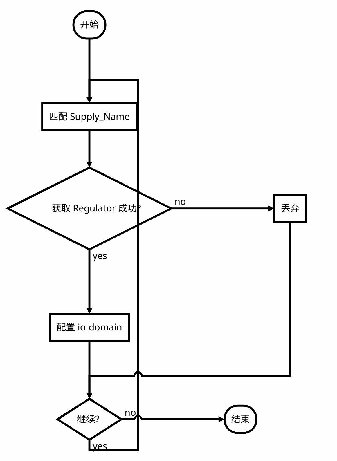
In probe, the driver uses the supply name to obtain the regulator defined under the corresponding supply name in DTS. It then configures the io-domain register from the regulator voltage: the bit is set to 1 for the 1.8v range and 0 for the 3.3v range.
Technical figure — 072, source CN PDF p.6, cn-p06-initialization-flow.png.
Flow: start → match Supply_Name → obtain regulator? If no, discard; if yes, configure io-domain. Continue? If yes, process the next supply; if no, finish.
3.2 Dynamic configuration
During initialization the driver binds to the regulator and registers a notifier. Whenever that regulator’s voltage changes, the notifier tells the io-domain driver to update the relevant register, enabling dynamic voltage-domain configuration.
4. Configuring io-domain
Not every IO power domain needs configuration: some have fixed voltages. The following three steps describe software configuration of io-domain.
4.1 Find the supply name in rockchip-io-domain.txt
The IO power domains requiring DTS configuration are described in Documentation/devicetree/bindings/power/rockchip-io-domain.txt in the Linux kernel tree. A domain may have different names in the TRM and hardware schematic; this binding document maps those names.
For RK3399, the source text lists bt565, audio, sdmmc, gpio1830 and pmu1830 in PMUGRF. The binding excerpt below uses bt656-supply, not bt565; this source discrepancy is retained. The phrase ‘The supply connected to ***_VDD’ identifies the corresponding schematic rail.
Possible supplies for rk3399:
bt656-supply: the supply connected to APIO2_VDD.
audio-supply: the supply connected to APIO5_VDD.
sdmmc-supply: the supply connected to SDMMC0_VDD.
gpio1830-supply: the supply connected to APIO4_VDD.
Possible supplies for rk3399 pmu-domains:
pmu1830-supply: the supply connected to PMUIO2_VDD.
4.2 Find the actual domain voltage in the schematic
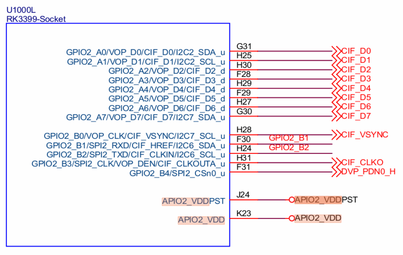
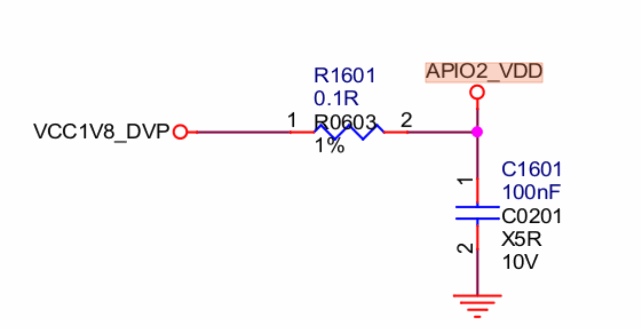
Using the RK3399-EVB schematic and bt656 domain as an example, the binding maps bt656 to APIO2_VDD. Tracing APIO2_VDD in the schematic shows that it is supplied by VCC1V8_DVP from RK808.
Technical figure — 072, source CN PDF p.7, cn-p07-figure1.png.
Technical figure — 072, source CN PDF p.8, cn-p08-figure1.png.
4.3 Configure DTS
With the supply name and physical source identified, locate the regulator vcc1v8_dvp in DTS and add bt656-supply = <&vcc1v8_dvp>; in rk3399-evb.dtsi. Configure other domains in the same way.
5. Domains controlled by hardware pins are normally left unconfigured
Some Rockchip IO domains are already controlled by a hardware pin. The kernel DTS normally does not configure them, so the existing hardware state is preserved. Flash and eMMC IO domains are commonly controlled this way.
The TRM register descriptions identify domains controlled by pins and explain how the pin’s input voltage determines the domain configuration. Configuration through GRF is the alternative, giving two possible control methods.
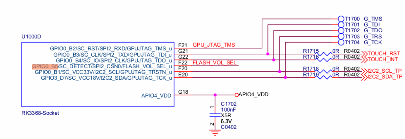
For example, the RK3368 TRM and RK3368-EVB schematic contain the following register and hardware-pin definitions.
TRM register descriptions:

Technical figure — 072, source CN PDF p.8, cn-p08-figure2.png.
Editable transcription of the visible source figure; headers are editorial, register values are unchanged.
| Bit | Access | Reset | Field / meaning |
|---|---|---|---|
| 14 | RW | 0x0 | flash_poc_control Flash IO domain POC control selection 0: controlled by gpio_0b5 pad 1: controlled by bit 2 of IO_VSEL |

Technical figure — 072, source CN PDF p.8, cn-p08-figure3.png.
Editable transcription of the visible source figure; headers are editorial, register values are unchanged.
| Bit | Access | Reset | Field / meaning |
|---|---|---|---|
| 2 | RW | 0x1 | flash0_v18sel FLASH0 IO domain 1.8V voltage selection 1’b0: 3.3V/2.5V 1’b1: 1.8V |
Hardware schematic:
Technical figure — 072, source CN PDF p.9, cn-p09-figure1.png.
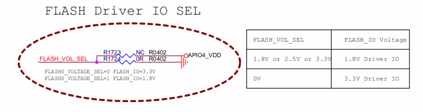
Technical figure — 072, source CN PDF p.9, cn-p09-figure2.png.
Editable transcription of the visible source figure; headers are editorial, register values are unchanged.
| FLASH_VOL_SEL | FLASH_IO Voltage |
|---|---|
| 1.8V or 2.5V or 3.3V | 1.8V Driver IO |
| 0V | 3.3V Driver IO |
The schematic also labels FLASH_VOLTAGE_SEL=0 FLASH_IO=3.3V and FLASH_VOLTAGE_SEL=1 FLASH_IO=1.8V. These are source circuit annotations, not universal pin tolerances.
6. Handling a regulator missing from DTS
If the relevant regulator cannot be found, the design may use no PMIC and instead connect a simple fixed supply. Add fixed-regulator definitions to DTS. Usually two regulators, 3.3v and 1.8v, are enough.
The following example is from rk3229-evb.dts. Determine whether the actual hardware uses 1.8v or 3.3v, then select the matching regulator:
    regulators {
       compatible = "simple-bus";
       #address-cells = <1>;
       #size-cells = <0>;
       vccio_1v8_reg: regulator@0 {
           compatible = "regulator-fixed";
           regulator-name = "vccio_1v8";
           regulator-min-microvolt = <1800000>;
           regulator-max-microvolt = <1800000>;
           regulator-always-on;
       };
       vccio_3v3_reg: regulator@1 {
           compatible = "regulator-fixed";
           regulator-name = "vccio_3v3";
           regulator-min-microvolt = <3300000>;
           regulator-max-microvolt = <3300000>;
           regulator-always-on;
       };
    };
&io_domains {
    status = "okay";
    vccio1-supply = <&vccio_3v3_reg>;
    vccio2-supply = <&vccio_1v8_reg>;
    vccio4-supply = <&vccio_3v3_reg>;
};
7. Frequently asked questions
7.1 Check whether a pin’s domain register is correct
An unexpected pin voltage may indicate a power-domain configuration problem. For example, on RK3399 software sets GPIO2_B1 high, but the measured voltage is wrong. If register reads confirm GPIO mux mode and a high output, io-domain may be misconfigured. Check the domain register by reversing the configuration steps described above.
First identify the domain from the schematic or datasheet. In this RK3399 example GPIO2_B1 belongs to APIO2_VDD, connected to VCC1V8_DVP.
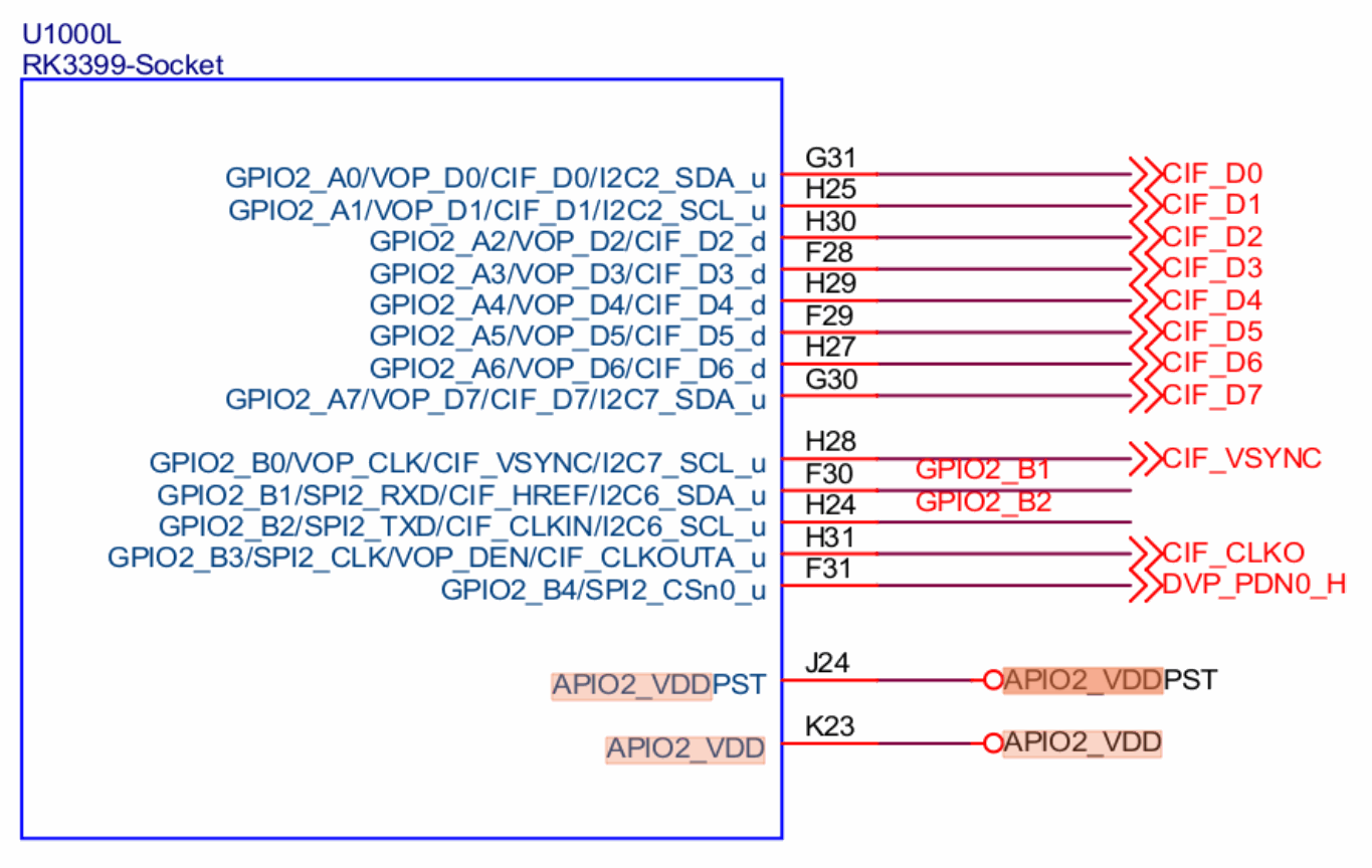
Technical figure — 072, source CN PDF p.10, cn-p10-figure1.png.
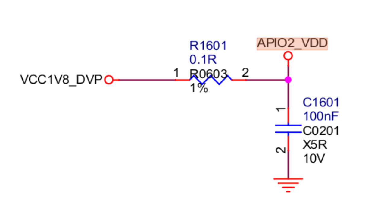
Technical figure — 072, source CN PDF p.11, cn-p11-figure1.png.
Find the corresponding software name in rockchip-io-domain.txt; here the domain name is bt656.
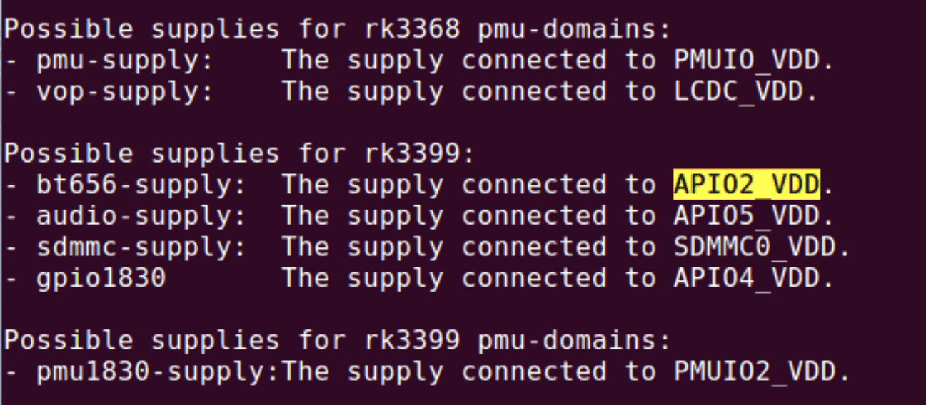
Technical figure — 072, source CN PDF p.11, cn-p11-figure2.png.
Copyable binding excerpt from the screenshot (the source writes gpio1830 without a -supply suffix or colon; do not silently normalize it):
Possible supplies for rk3368 pmu-domains:
- pmu-supply:    The supply connected to PMUIO_VDD.
- vop-supply:    The supply connected to LCDC_VDD.

Possible supplies for rk3399:
- bt656-supply:  The supply connected to APIO2_VDD.
- audio-supply:  The supply connected to APIO5_VDD.
- sdmmc-supply:  The supply connected to SDMMC0_VDD.
- gpio1830      The supply connected to APIO4_VDD.

Possible supplies for rk3399 pmu-domains:
- pmu1830-supply:The supply connected to PMUIO2_VDD.
RK3368 PMU domains map pmu/vop to PMUIO_VDD/LCDC_VDD. RK3399 maps bt656/audio/sdmmc/gpio1830 to APIO2_VDD/APIO5_VDD/SDMMC0_VDD/APIO4_VDD; its PMU supply maps to PMUIO2_VDD.
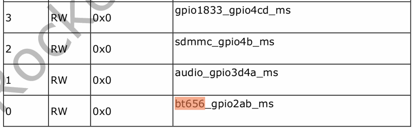
Locate the register in the TRM and read it with io or another suitable tool; the base is normally GRF or PMUGRF. Here bt656 is bit0 at offset 0xe640, with GRF base 0xff770000. Run io -4 0xff77e640 in the serial terminal. If bit0 is 1, the configured range is 1.8v, consistent with VCC1V8_DVP and the DTS entry is correct. If bit0 is 0, it selects 3.3v, inconsistent with VCC1V8_DVP, so the entry is wrong. These addresses apply to the source’s RK3399 example, not arbitrary boards.
Technical figure — 072, source CN PDF p.11, cn-p11-figure3.png.
Editable transcription of the visible source figure; headers are editorial, register values are unchanged.
| Bit | Access | Reset | Field / meaning |
|---|---|---|---|
| 3 | RW | 0x0 | gpio1833_gpio4cd_ms |
| 2 | RW | 0x0 | sdmmc_gpio4b_ms |
| 1 | RW | 0x0 | audio_gpio3d4a_ms |
| 0 | RW | 0x0 | bt656_gpio2ab_ms |
The screenshot shows gpio1833_gpio4cd_ms, whereas the binding screenshot uses gpio1830; retain both source spellings and verify against the matching TRM/BSP.
7.2 Incorrect io-domain registers
Common causes of an incorrect register configuration include:
The configured regulator voltage is wrong.
The regulator is not configured or not enabled.
The regulator loads later than the io-domain driver, so obtaining it fails.